Background-Suppressed High-Throughput Mid-Infrared Photothermal Microscopy via Pupil Engineering
ABSTRACT
Mid-infrared photothermal (MIP) microscopy has been a promising label-free chemical imaging technique for functional characterization of specimens owing to its enhanced spatial resolution and high specificity. Recently developed wide-field MIP imaging modalities have drastically improved speed and enabled high-throughput imaging of micron-scale subjects. However, the weakly scattered signal from sub-wavelength particles becomes indistinguishable from the shot-noise as a consequence of the strong background light, leading to limited sensitivity. Here, we demonstrate background-suppressed chemical fingerprinting at a single nanoparticle level by selectively attenuating the reflected light through pupil engineering in the collection path. Our technique provides over three orders of magnitude background suppression by quasi-darkfield illumination in epi-configuration without sacrificing lateral resolution. We demonstrate 6-fold signal-to-background noise ratio improvement, allowing for simultaneous detection and discrimination of hundreds of nanoparticles across a field of view of 70 µm x 70 µm. A comprehensive theoretical framework for photothermal image formation is provided and experimentally validated with 300 and 500 nm PMMA beads. The versatility and utility of our technique are demonstrated via hyperspectral dark-field MIP imaging of S. aureus and E. coli bacteria.
Contributed equally to this work. \altaffiliationContributed equally to this work. \alsoaffiliationDepartment of Biomedical Engineering, Boston University, Boston, MA 02215, USA \alsoaffiliationDepartment of Biomedical Engineering, Boston University, Boston, MA 02215, USA
1 KEYWORDS
photothermal imaging, chemical imaging, nanoparticle detection, biosensing, bacteria detection, infrared spectroscopy
2 INTRODUCTION
Vibrational spectroscopic imaging has been an essential tool for molecular fingerprinting in biological and medical sciences 1. Intrinsic molecular vibrations in specimens can be utilized as contrast by either optical absorption or inelastic Raman scattering. Therefore, the vibrational signal avoids challenges associated with fluorescence labels such as sample perturbation, photo-bleaching, and phototoxicity. The spontaneous Raman scattering spectromicroscopy offers sub-micron spatial resolution but the non-linear process limits sensitivity and acquisition speed 2. To boost the imaging speed, coherent Raman scattering microscopy is developed 3, 4. Historically, Fourier transform infrared (FTIR) microscopy has been one of the most prevalent chemical analysis tools in various fields 5, 6. However, FTIR has a low spatial resolution of several microns due to the diffraction limit of the long illumination wavelengths in the mid-IR region (2.5 - 25 µm). Such resolution is insufficient to study intra-cellular structures inside a biological cell. Atomic force microscope infrared spectroscopy (AFM-IR) techniques beat this inherent resolution limit 7, 8 by detecting thermal expansion with an AFM tip and nanoscale (20 nm) resolution has been achieved 9. Yet, the slow scanning process in AFM-IR limits imaging throughput. Additionally, applying AFM-IR to a liquid sample is very difficult, which limits its applications to characterize live cells. To tackle these challenges, mid-infrared photothermal (MIP) microscopy was recently developed, where vibrational absorption-induced chemical contrast was detected by a visible probe beam 10, 11, 12. After the initial inception in 2016 10, MIP has been progressively evolving from the proof of concepts to commercialization and wide applications 13, 14, 15, 16. Technically, Delong Zhang et al. first demonstrated sub-micron resolution mid-IR spectroscopic imaging of living cells and organisms with a point scanning approach in transmission mode 10. An epi-detection MIP was subsequently developed to extend the system capability to opaque samples including drug tablets 12. The photothermal imaging in counter propagation detection geometry was also developed to employ high-NA objectives for high-resolution ( 300 nm) and sensitive chemical detection down to 100 nm polystyrene beads at the high-temperature rise (30 to 45 K) 11, 17, 18 and demonstrated in material science application19, 20. More recently, confocal Raman spectroscopy is integrated into MIP 21, providing complementary chemical information by simultaneous Raman and IR spectroscopy of specimens at co-registered sub-micron spatial resolution. Alternatively, mid-IR vibrational signatures have been extracted using a near-IR 22 or shortwave IR laser probe 23.
Despite its high sensitivity, the scanning MIP microscopy approaches have three main challenges: (i) Limited imaging speed due to the pixel-by-pixel acquisition; (ii) Wavelength dependent focused spot size mismatch between the IR and visible beams; (iii) Mechanical instabilities and sample drift. Harnessing complementary metal-oxide-semiconductor (CMOS) cameras that provide ultra-sensitive (>70 dB) and high-speed image (100s FPS) capturing at very low-cost, very recently introduced wide-field MIP systems 24, 25, 26, 27, 28, 29 enabled high-throughput chemical imaging with a significant speed improvement. Bai et al. 24 developed a virtual lock-in camera technique to detect the photothermal induced interferometric reflectance change of sample placed on a silicon substrate. Similarly, Schnell et al. 29 reported an interferometric method for measuring surface thermal expansion on histopathology slides using a special common-path interferometry objective, namely, Mirau objective along with an extremely high full-well capacity camera (2 million e-). Moreover, quantitative chemical phase microscopy of living cells has been demonstrated by reconstructing a very minute optical phase path length difference 25, 27, 28. Despite these recent advancements, wide-field MIP imaging of single sub-wavelength particles such as bacteria and viruses has not been demonstrated. A major limitation is that these techniques rely on bright-field sample illumination in which weakly scattered light from sub-wavelength (<500 nm) structures are overwhelmed by the large background arising from the strong illumination field. As the particle size decreases, the photothermal signal becomes buried under the background shot-noise from this unperturbed illumination. Thus, chemical imaging of nanoparticles becomes very difficult to achieve.
Here, we reported a background-suppressed wide-field MIP microscope via dark-field geometry in the epi-illumination configuration without sacrificing resolution. Background suppression via dark-field geometry has been proved to drastically improves the signal-to-background ratio such that the camera captures only the scattered light 30. The dark-field illumination in the epi-configuration is achieved by selectively blocking the back-reflected light in the collection arm after the objective. Our approach obviates the need for special objectives or condensers as in the off-the-shelf dark-field microscopes 31. The dark-field illumination through the objective can be performed via oblique illumination which is blocked using a field stop 32, 33 and on-axis illumination which is blocked by a rod mirror 34 or a circular stop 35. The objective-type on-axis dark-field illumination blocks only the small fraction of the objective numerical aperture (NA), low-NA part centered around the optical axis. Such illumination can employ high-NA objectives compared to that of the oblique, allowing for more sensitive and high-resolution detection of the back-scattered light from small specimens down to single fluorescent molecules 35. In this study, we illuminate the sample with a nearly collimated beam which is refocused at the objective back pupil after the specular reflection from the substrate surface. A custom fabricated blocker filters out this beam at the pupil’s conjugate plane, thus, nearly no reflected light reaches the camera. We demonstrate more than 6-fold signal-to-background noise ratio improvement over a large field of view (FOV) of 70 µm 70 µm, enabling simultaneous photothermal imaging of hundreds of particles at once. We establish a complete physical model for the photothermal image formation that utilizes boundary element methods and angular spectrum representation framework. The theory is experimentally validated with 300 and 500 nm PMMA beads. We further provide the transient temperature response for these beads by employing the time-gated pump-probe approach 25. To highlight its potential for biological applications, we demonstrate fingerprinting of single E. coli and S. aureus in the wide-field sense. Our method advances high-throughput nanoparticle imaging and characterization with chemical specificity at a single particle level.
3 RESULTS AND DISCUSSION
3.1 Photothermal contrast mechanism in dark-field MIP
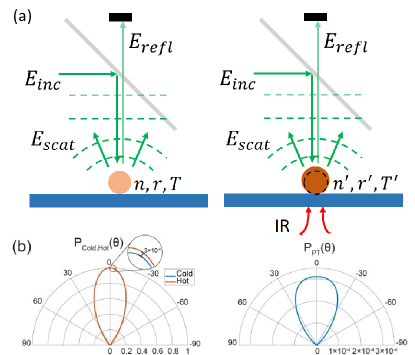
Figure 1 shows the photothermal contrast mechanism in dark-field illumination MIP microscopy. A visible laser beam illuminates the sample placed on top of a silicon substrate in the epi-configuration (see Figure 1a). The incident field scatters off the sample and reflects from the substrate surface . The superposition of incident and reflected light constitutes the total driving field of this scattering process. The scattered field is proportional to its optical parameters including refractive index (n) and size (r) along with the illumination wavelength (). The dark-field illumination rejects 103 of the reflected light in the collection path such that only the scattered fields reach the detector. A mid-infrared laser beam vibrationally excites the sample owing to the absorption bonds at the IR illumination wavelength. The IR absorption generates heat and increases the sample’s temperature by . This photothermal effect results in a change in the samples refractive index and size which depends on the sample’s thermo-optic () and thermal-expansion () coefficients at pre-IR pulse temperature and hence the scattered field. To obtain the photothermal signal, the scattering difference between IR-on and IR-off states is measured. We refer to IR pulse on and off states as respectively, “hot” and “cold” frames throughout the manuscript. Figure 1b shows the normalized radiation profiles of scattering from a 500 nm PMMA bead on the silicon substrate. The zoom-in region indicates a very subtle signal difference ( 0.03% for ) between the “hot” and “cold” states. It is evident that the photothermal radiation profile has a broadened angular distribution compared with the scattering profiles. This suggests a careful treatment of image formation considering imaging optics is required for accurate photothermal signal modeling. With that, theoretical analysis of illumination and collection engineering can be carried out to achieve sensitivity and resolution improvement in the imaging system.
3.2 Theory
In dark-field illuminated epi-detection configuration, only the back-scattered light from the particle within the angular range of the objective lens’ numerical aperture is collected. The camera captures the resulting scattered field as intensity images (). The IR absorption induced change in refractive index (n) and particle size (r) modifies the scattered field. The scattering field change is typically three orders of magnitude smaller than the pre-IR pulse scattered amplitude (). With this assumption, the photothermal signal can be approximated as follows:
| (1) |
This result shows that is detected through interference with its own scattered field . This is similar to the interferometric detection of photothermal signal which detects with a reference field such that photothermal signal becomes 36. One might expect that both detection schemes could achieve similar sensitivity. Yet, the dark-field photothermal signal has a larger amplitude for a given number of total collected photons due to the fact that the amplitude of scales with the which is much smaller in the interferometric detection case. The enhancement factor over interferometric detection scales with the ratio between the scattered and reflected fields (), which determines the signal contrast in such condition 37, 38, 39. Therefore, one can improve the photothermal signal by reducing the background while keeping the detector at the saturation level. We note that this improvement is only valid for in the bright-field illumination (see Supplementary 1 Section 1 for details). To obtain a generalized photothermal signal quantification, we use modulation depth which is defined as a fractional change in the scattered intensity (). can be approximated as in narrow temperature intervals. This assumption implies that the photothermal signal scales linearly with the for a known specimen. Therefore, one can infer the temperature change distribution of detected particles using a priori knowledge of the sample’s physicochemical parameters (see Supplementary 1 section 2).
The scattering-based measurements could bring the system into the shot-noise limited regime where all other noise sources, i.e, electronic and thermal, are negligible if the scattering intensity can saturate the detector at a reasonable exposure time. The shot-noise-limited detection is typically granted for bright-field detection in which a strong reference field enhances the weak scattering signal37. Yet, the particles of interest in this study generate enough scattered photons to bring the camera into the shot-noise-limited regime at a few milliseconds exposure time in the dark-field detection. The noise-floor in a single measurement is then dominated by the photon noise of photoelectrons accumulated at the detector during the integration time. This is a valid assumption for particles that generates enough photons () to saturate the detector within a given short exposure time. The shot-noise fluctuation is equal to the standard deviation of the detected photons . In such case, the signal-to-noise ratio (SNR) in the dark-field photothermal signal detection becomes,
| (2) |
The constant comes from the fact that the noise in hot and cold images are independent of each other and hence the subtracted image noise scales with the . The modulation depth limits the sensitivity in a single shot. From Eq. 2, the modulation depth should satisfy to be detected in a single frame. The maximum is bounded by the camera sensor’s pixel well depth (). Therefore, large pixel depth cameras are desirable in shot-noise-limited measurements. Furthermore, the frame averaging is typically employed to increase SNR which is necessary to detect the very subtle scattered field change.

3.3 Pupil engineering for objective-type dark-field illumination
The experimental setup is illustrated in Figure 2. The IR beam is provided by a tunable QCL (quantum cascade laser, MIRcat, Daylight solutions). The green pump beam ( = 520 nm central wavelength, = 9 nm bandwidth) is obtained by the second-harmonic generation of a quasi-continuous femtosecond laser (1040 nm, 100 fs, 80 MHz, Chameleon, Coherent) using a non-linear crystal. Such a short pulse provides a low-temporal coherence length of 30 µm, yielding nearly speckle-free sample illumination. The femtosecond beam is chopped to pulses (100 ns pulse width) by an acousto-optical modulator (AOM, Gooch and Housego) before entering the non-linear crystal. The optical power after the SHG crystal becomes approximately 30 mW at the continuous AOM operation. The IR beam is weakly focused on the sample from the backside by a parabolic mirror (f = 15 mm, MPD00M9-M01, Thorlabs), illuminating nearly the FOV of 70 µm 70 µm. We chose silicon as a substrate for two reasons: (1) silicon is transparent at the IR range and (2) back-scattered light intensity from a particle on the silicon substrate is about 10 times larger compared with a glass substrate (see supplementary Figure S3). The latter comes from the fact that silicon reflectively is much larger than glass. The strong forward scattering from large dielectric nanoparticles can be collected more on top of a silicon substrate in epi-detection, achieving better collection efficiency given the illumination power. The IR illumination is delivered from the backside of the silicon substrate. The p-polarized IR beam is obliquely incident at a angle to increase the transmission rate utilizing Brewster’s angle (see Supplementary 1 Section 3 for details). Moreover, the oblique illumination avoids the IR absorption by the objective lens. The probe beam is employed in the Köhler illumination configuration where the collimated laser is focused on the back focal plane of the objective lens (50, 0.8 NA, Nikon) by a condenser (f = 75 mm, AC254-075-A, Thorlabs). This provides wide-field plane wave illumination of the sample. Due to the power loss along the optical path and AOM chopping (1:50), 0.6 mW probe power illuminates the sample across the FOV of 190 µm 190 µm. The objective lens is mounted on a piezo stage (MIPOS 100 SG RMS, Piezosystem Jena) for fine focus adjustment. Besides, the piezo scanner eliminates the need for defocus adjustment of the IR beam, since the sample z position remains unchanged with respect to the IR focus plane.
The objective-through dark-field illumination is implemented through pupil engineering at the objective pupil’s conjugate plane. To achieve this, the objective pupil is relayed by a unit magnification 4f system that uses two identical achromatic doublets (f = 100 mm, AC508-100-A, Thorlabs). As shown in Figure 2a, the left focal plane of this 4f system (Fourier plane) becomes conjugate to the objective pupil. Since the back-reflected light from the substrate is refocused at the objective back pupil, the reflected light at the conjugate plane becomes accessible. This approach is based on the Unlu’s group earlier study in which contrast-enhanced interferometric detection is demonstrated by attenuating a small fraction ( 20:1) of the reflected light 40. To enable the dark-field detection, we instead block a large amount (1000:1) of the reflected light by a custom fabricated pupil mask placed into this Fourier plane. The pupil mask is depicted in Figure 2b. There is a dot blocker with a diameter of 1.6 mm at the center of the mask. This only filters the low-NA portion (0.2 NA) centered around the objective optical axis. The center block dot;s diameter is empirically determined by considering the amount of collected scattered photons as well as the alignment difficulty. The blocker blocks 6% of the pupil while passing a large fraction of the collected scattered light. The supplementary Figure S5 shows the block diameter as a function of the collected power for both intensity-only and photothermal cases. According to simulation results, we estimate 83.7% collection efficiency for the 500 nm beads on a silicon substrate. Therefore, the pupil mask can provide dark-field illumination of wavelength size particles while maintaining the detector at shot-noise-limit operation. As we pointed out earlier, the photothermal effect broadens the angular distribution of the radiation, yielding a lower directivity compared to the DC signal. Consequently, the collected photothermal power is 89% for the 1.6 mm blocker, which has 5.3% higher efficiency than the DC case. One can also choose a smaller pupil diameter as long as the blocker overfills the back-reflected light at the Fourier plane. In ideal conditions, the minimum blocker size is equal to the relay magnification times the focused/imaged beam size at the objective back pupil. In practice, the beam divergence, optical aberrations, and system misalignment incur a larger beam size. Furthermore, we expect better collection efficiency for smaller particles since they have much broadened angular distribution owing to the Rayleigh scattering 41. This result also indicates that photothermal modulation depth at high scattering angles becomes larger. Besides, our method can be implemented on most of the standard bright-field objectives which offer a wide range of availability for different applications. This obviates the need for high-cost special objectives which have the dark-field ring at their back-pupil. The dark-field ring blocks the high-NA part of the objective, reducing the attainable resolution. Therefore, our technique does not possess challenges associated with the dark-field objectives for epi-detection. In the implementation, an absorptive material, Titanium, is deposited at the center of optic quality quartz. The titanium thickness is about 80 nm, providing an optical density of 3. This is almost opaque ( 0.1% transmission) compared to the 80% for the glass region. We note that there is still a small fraction of the reflected light reaching the detector, allowing for quasi-darkfield illumination. After the pupil mask, the dark-field image is formed on a CMOS camera (BFS-U3-17S7, FLIR, dynamic range of 72.46 dB, dark noise of 22.99 e-) by a tube lens (f = 200 mm, TTL200-A, Thorlabs). The camera region-of-interest is cropped to match the IR spot size at the sample. The camera exposure time during the experiments is set to a level that nearly saturates the camera pixels. In summary, our dark-field illumination scheme provides robust, simple, and low-cost background suppression for contrast enhancement in the epi-detection arrangement.
3.4 Time-gated virtual lock-in camera detection
Photothermal images are acquired by using the virtual lock-in camera detection 24. Figure 2c shows the synchronization control of the system. A pulse generator (Emerald Pulse Generator, 9254-TZ50-US, Quantum composers) generates the master clock signal at 200 kHz and externally triggers the QCL, AOM, and CMOS camera to synchronize the IR pulses, probe pulses, and camera exposure. The pulse generator has a division function that enables separately controlling the duty cycle, frequency, amplitude, delay, and width at each output channel. The output waveforms are set to pulse wave. The time delay () between the IR and visible pulses is controlled to measure transient photothermal response via a time-gated pump-probe approach 25. We used the AOM channel at the normal mode without changing the duty cycle. The QCL and camera channels are set to the duty cycle mode to create hot and cold frames. The QCL pulse train is chopped electronically at 50% duty cycle, that is, every other 1000 IR pulses on and off. Similarly, the camera channel duty cycle is set to 2% to achieve a 400 Hz frame rate at the region of interest. The camera readouts “hot” and “cold” frames sequentially and streams to the computer via USB. The pre-determined frame averaging is processed in real-time for computational efficiency, significantly reducing the memory requirements at a large number of frames (), where N is the frame number). To avoid probe laser intensity fluctuations, each image is normalized by the average intensity at a predetermined reference region which is obtained by directly reflecting the split illumination beam to the lower left of the FOV. During the image acquisition, we set the odd- and even-numbered frames as “hot” and “cold” states, respectively. This allows us to extract photothermal signal sign which has size dependency detailed in the results sections. The photothermal image is then obtained by subtracting the “hot” and “cold” images as shown in Figure 2d. A custom-written Python code is developed to automatically control pulse delay, piezo scanner, image acquisition, and processing (detailed in Supplementary 1 section 5).
3.5 Experimental verification of contrast enhancement
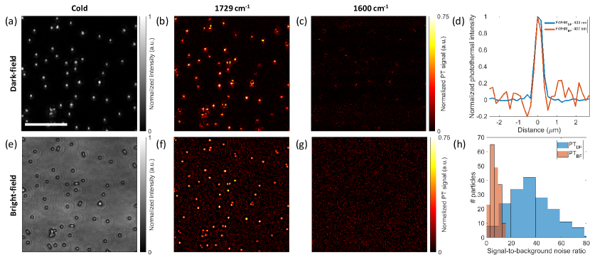
Proof-of-principle experiments for contrast enhancement are demonstrated on 500 nm Polymethyl methacrylate (PMMA) beads. The PMMA beads present an ideal model for the system characterization since they resemble the particle size and dielectric () characteristics of bacteria used in our study. Figure 3 compares the dark-field and bright-field imaging results. The dark-field illumination is achieved by placing the blocker mask at the pupil conjugate plane detailed in the instrumentation section. For a fair comparison, bright-field imaging results are obtained by the same setup at the same conditions without the pupil mask. The exposure time in both cases is adjusted to bring the camera to the saturation level. As shown in Figure 3a,e, the dark-field illumination provides background-free DC imaging while the bright-field image has a non-zero background caused by the reflection from the silicon substrate. Although the non-zero background in the DC images can be canceled by subtraction, it still contributes to shot-noise which limits the maximum attainable SNR from a single frame. Figure 3f shows the background shot-noise clearly, which degrades the visibility of the PMMA beads. In the dark-field photothermal image (Figure 3b), the background shot noise is significantly eliminated. The cross-section profiles of the bead shown in Figure 3d further emphasize this significant background noise suppression. The resolution capability of the imaging system can be also calculated from these cross-sections. The full-width-half-maximum (FWHM) of a 500 nm bead is 433 nm for the dark-field imaging and 407 nm for the bright-field imaging. This result shows that our dark-field illumination approach can achieve the nearly same resolution as in the bright-field illumination. One can expect that the dark-field FWHM would be smaller due to the fact that the interferometric signal in the bright field case has a broader point spread function (PSF). However, the 500 nm PMMA bead scattered intensity has still a contrast level comparable to the interferometric signal, providing a sharper PSF than that of the interference term. We anticipate that the dark-field detection will provide better resolution for much smaller nanoparticles (100 nm PMMA beads) which have much weaker contrast in the bright-field imaging. After a Gaussian deconvolution with the particle size, we obtained 353 nm lateral resolution which is close to the theoretical = 325 nm resolution value. The experimental FWHM is slightly larger than the theoretical resolution value because the 500 nm bead is not small enough to be approximately treated to be a point source. To obtain a more quantitative analysis metric, the signal-to-background-ratio histograms of 190 PMMA beads are compared in Figure 3h. The median signal-to-background-noise ratio for the dark-field case is about 6 times larger than the bright-field case, reaching up to 100. The signal-to-background-noise improvement of this dark-field illuminated MIP imaging system has been demonstrated for high-throughput chemical imaging of wavelength size single particles.
3.6 Experimental validation of theoretical calculations
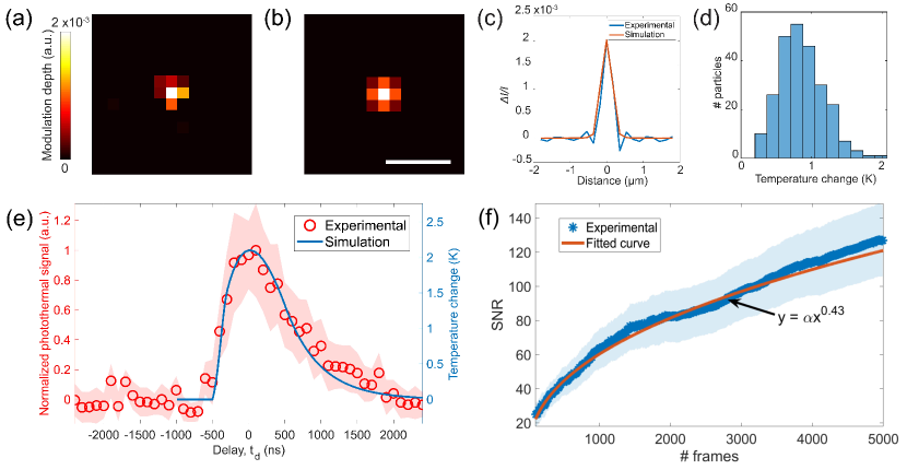
The image formulation framework detailed in the Methods section is verified in two steps using the experimental photothermal image of a 500 nm PMMA bead. We first calculate the modulation depth from the BEM simulation using the PMMA’s optical and thermal coefficients at . Since the modulation depth can be linearly related to the small temperature changes, of the PMMA beads can be retrieved from the experimental results (see Supplementary 1 Section 2 for details). The experimental photothermal modulation depth image of a 500 nm PMMA bead on the silicon substrate is shown in Figure 4a. The modulation depth is calculated as the ratio between photothermal image and peak contrast value at the cold state. Figure 4b is a simulation photothermal modulation depth image which is scaled to the same maximum value in Figure 4a. The cross-section profiles in Figure 4c show consistency between the experimental and simulated results. We then calculate the histogram for all PMMA beads Figure 3b as shown in Figure 4d. The maximum temperature rising across the FOV is calculated as 2 K which is consistent with the COMSOL simulations (see Supplementary Section 4 for details).
The simulated temperature rising and the experimental photothermal signal versus delay scan of 56 individual PMMA beads with a 500 nm diameter is shown in Figure 4e. For each specific delay value, the photothermal signal is proportional to the integrated temperature change within the time window of the probe pulse, which has a 200 ns pulse width as introduced in the previous section. In other words, the curve shape of the experimental delay scan is a convolution of the simulated temperature curve with the 200 ns probe pulse. The experimental delay scan curve is not distorted too much compared to the simulation, which means the 200 ns pulse width is short enough to probe the highest temperature change. We point out that the transient response curves depend on sample size and IR pulse shape. Considering the pulse shape and particle size in this study, the time delay is carefully determined to obtain the maximum photothermal signal during the experiments. The photothermal images are then acquired using the optimized delay scan value that corresponds to the highest photothermal signal.
The photothermal signal scales linearly with the probe power in the shot-noise limit. A maximum SNR in a signal frame is then can be achieved at the camera saturation level where the shot-noise-limited detection is granted. The minute contrast change as a result of the photothermal effect can be detected through multiple frames averaging which reduces the noise floor by a factor of the square root of the number of averaged frames. Supplementary Figure S12 demonstrates the shot-noise limited operation for our camera and noise floor reduction by frame averaging. Figure 4f further shows the noise analysis of 56 PMMA beads over a different number of frames averaging . The noise is calculated as the standard deviation of the photothermal image background nearby the particles. The exponential fit to the experimental SNR values is found to be . The slight variation from the theoretical value of 0.5 could be attributed to the mechanical noise in the imaging system. The photothermal image results at different frame averaging have been also shown in supplementary Figure S13. Furthermore, we obtain a photothermal spectrum of 20 individual beads in the supplementary Figure S14. The IR wavenumber is scanned from 1750 to 1400 cm-1 with a step size 1 cm-1, requiring nearly 29 minutes of total acquisition time. The image acquisition and hyperspectral analysis are detailed in the supplementary information. The spectra show distinctive absorption peaks around the carboxyl group and C-H bonds with high spectral fidelity. Our experimental results are consistent with those obtained from the point-scan MIP imaging reported in 21. Overall, our characterization has shown the potential of dark-field MIP microscopy to facilitate highly sensitive hyperspectral imaging of wavelength size particles.
3.7 Size dependence of photothermal contrast
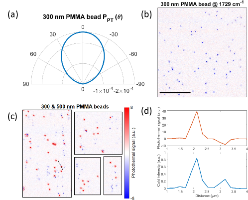
We next investigate the size dependence of photothermal signal using 300 nm PMMA beads in diameter. Figure 5a shows the scattering intensity polar plot of the photothermal signal from a PMMA bead of 300 nm diameter. The radiation spreads more uniformly across the angles, indicating a lower directivity compared with the 500 nm PMMA radiation profile in Figure 1b. This stems from the well-known Mie-scattering fact that far-field scattering angular distribution has a strong dependency on particle size. The directivity of the radiation is inversely proportional to the scatterer’s size. We note that both polar plots are normalized by the maximum intensity value at the cold state. More importantly, unlike the positive contrast in 500 nm PMMA beads, 300 nm PMMA beads have negative photothermal contrast. This could be explained by the self-interference between the back-scattered and forward scattered fields from the same particle. This self-interference of scattered fields occurs since the forward scattered fields from particles reflect from the substrate surface. The forward scattered light becomes less dominant for the smaller particles due to the Mie-scattering phenomena. Therefore, the photothermal contrast sign flip is likely to happen when the amplitude of the forward scattered field decreases. Another reason for the photothermal signal sign change comes from the fact that the refractive index and thermal expansion of PMMA beads counteract each other due to the opposite sign11. Interestingly, the photothermal signal contribution from these effects could cancel each other at a certain size depending on the magnitude of these thermal coefficients as well as the aforementioned phase relation between forward and backward scattered fields. Therefore, certain particles of interest depending on their size and material properties could be invisible which could eventually limit the certain applications in scattered-based MIP techniques 11. Due to the complexity of such analysis with a closed-form solution, we numerically investigate the size-dependent photothermal signal from a size range of PMMA beads on the silicon substrate in Supplementary Figure S15. The inversion for the PMMA bead occurs around 350 nm in diameter. We experimentally verified the sign inversion using a 300 nm PMMA bead sample. Figure 5b shows the photothermal image of the 300 nm PMMA beads with a signal-to-background-noise ratio of 44 at the frequency of 1729 cm-1. The cold state and off-resonance images at 1600 cm-1 are provided in supplementary Figure S13. We further cross-validate our theory using a mixed 300 and 500 nm PMMA beads sample (Figure 5c). Depending on the particle size, the photothermal signals from different particles yielded positive or negative contrast in a single FOV. Our experimental findings show great agreement with the theoretical predictions. The cross-section profiles in Figure 5d demonstrate a clearer comparison of scattered intensity and contrast flip. Due to the sixth power dependence (r6) of the scattered signal, 300 nm beads yield lower DC contrast. Moreover, the temperature rise for smaller particles becomes less due to a faster thermal decay in the orders of a few hundreds of nanoseconds, requiring shorter pump and probe pulse widths (Supplementary Figure S16). As a result, lower photothermal SNR for 300 nm beads is obtained. To obtain high SNR images with good data fidelity in these proof-of-concept experiments, the number of frame averaging is increased by five-fold to 5000.
3.8 Fingerprinting single bacteria
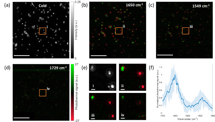
To demonstrate the utility of our method on biological specimens, we study two bacteria species with various sizes and shape distribution. The bacteria are directly immobilized on the silicon substrate at room temperature (Supplementary 1 Section 5). We first imaged spherical S. aureus bacteria in the fingerprint region. Figure 6a demonstrates cold image in which the single S. aureus cells appear to be round. The intensity variation across the bacteria indicates size differences of S. aureus cells. When IR frequency is tuned to the amide band at 1650 cm-1, which is a characteristic band in proteins, the bacteria show high-contrast photothermal signal with a signal-to-background-noise ratio of 93 (Figure 6b). The photothermal image indicates the rich protein in S. aureus cells. The photothermal contrasts from different bacteria cells show not only amplitude variation due to scattered intensity differences but also negative or positive contrast depending on their size. These observations are consistent with the one obtained from the PMMA beads above. We then pinpointed another major protein band of amide at 1549 cm-1 (Figure 6c). In contrast to amide , amide generates lower photothermal contrast owing to the weaker absorption. When IR is tuned 1729 cm-1, associated with C=O bond which is abundant in lipids, a very weak contrast is observed as a result of low lipid content in the S. aureus (Figure 6d). Furthermore, Figure 6e shows spectrum of 12 individual bacteria from 1700 to 1500 cm-1 with a step size of 1 cm-1. Our results show agreement with the previously reported study using the point-scan MIP 21. With these results, single bacteria fingerprinting in a wide-field imaging system has been demonstrated. Owing to the wide-field detection, simultaneous photothermal detection of tens of bacteria is achieved.

Next, we demonstrated hyperspectral characterization of rod-shaped E. coli bacteria in the fingerprint region. Figure 7a shows scattered intensity image of E. coli. Unlike the S. aureus bacteria, the intensity variation across the many E. coli bacteria is small. This suggests that the diameter of each E. coli bacterium is almost monodisperse. Figure 77b-d compare photothermal images of amide , amide , and off-resonance bands at frequencies of 1650 cm-1, 1549 cm-1, and 1729 cm-1 respectively. We obtained about four-fold lower photothermal signal compared with the large S. aureus cells due to the smaller diameter of E. coli bacteria. The photothermal contrast at the bacteria center is always positive owing to their uniform diameter distribution. We further obtain spectra of 10 bacteria (Figure 7e) from 1700 to 1500 cm-1 with a step size of 1 cm-1. The E. coli and S. aureus spectra show different curves across the amide and bands. These observations lead to potential applications in high-throughput single bacteria characterization and classification.
4 CONCLUSION
We have introduced a contrast-enhancement method in wide-field MIP microscopy with pupil engineering that enables dark-field illumination through a bright-field high-NA objective. We achieved three orders of magnitude background suppression in DC images while maintaining diffraction-limited lateral resolution. Our dark-field illuminated MIP technique improved the signal-to-background ratio at least 6-fold over a large FOV of 70 by 70 µm that allows for high-throughput and sensitive chemical imaging of hundreds of sub-micron particles simultaneously. We showed the transient temperature response of 500 nm PMMA nanoparticles at sub-200 ns temporal resolution via a time-gated pump-probe approach implemented on a commercially available CMOS camera. We experimentally demonstrated hyperspectral imaging of single S. aureus and E. coli bacterium in the fingerprint region with high SNR and high spectral fidelity in both experiments. Single sub-micron bacterium fingerprinting in a wide-field manner has been demonstrated. Moreover, a comprehensive analytical model for photothermal contrast mechanism and image formation was described and experimentally validated. This physical model opens up further advancements in photothermal microscopy through careful signal characterization with the optical system’s constituent specifications, including point spread function, illumination and collection functions, and substrate.
We note that an independent study using a similar background suppression concept has been recently reported during the peer-review process of our work 42. Toda et al. used the dark-field scheme to expand the dynamic range in mid-IR photothermal quantitative phase imaging. Dark-field detection in transmission mode is realized by attenuating the strong bright-field illumination at the pupil conjugate plane by a dot blocker. Dynamic range expansion of quantitative phase imaging of micrometer-scale specimens such as 5 µm silica beads and COS cells has been successfully demonstrated. This phase imaging study used specimens that are much larger than the illumination wavelength, requiring a low-refractive-index difference between the surrounding medium. Therefore, single nanoparticle detection sensitivity is still challenging. Despite the methodical similarity, detection mechanism, imaging configuration, and sensitivity draw major differences. First, detection principles of sub-diffraction-limited nanoparticles rely on elastically scattered light. Second, we demonstrate 10-fold enhanced scattered light detection using silicon substrate in epi-illumination configuration which is critical for successfully suppressing the background without compromising from illumination power. Third, our scope of work is to study nanoscale specimens with high optical detection sensitivity down to a single 300 nm nanoparticle.
The dark-field illumination could be a natural choice for specimens that scatters enough photons to saturate the camera. There are two drawbacks to this approach. First, it does not benefit large particles that can already generate high image contrast in bright-field illumination or dense specimens such as cells and tissues that generates large background signal. Therefore, our method is well suited for individual particles sparsely distributed across the substrate. This will be of significant importance for enabling chemical characterization at the single-particle level for understanding variations in the diverse nanoparticle populations. The other limitation is the strong (sixth-power) size dependence of the scattering intensity (r6) which significantly drops for sub-100 nm nanoparticles. Therefore, the applications are limited to the wavelength scale of individual particles to maintain shot-noise limited detection. To push the sensitivity limit down to a single virus or exosome, common-path interferometric detection of the scattered light in tandem with pupil engineering could be a path forward in future wide-field MIP studies 40, 38. This will not only improve the imaging system’s sensitivity but also the lateral resolution down to 150 nm 43. Together, our theoretically supported wide-field MIP microscopy technique could bring exciting applications in life sciences.
5 MATERIALS AND METHODS
5.1 Image field calculations
To accurately characterize the photothermal contrast mechanism, we developed an analytical model considering imaging optics and system parameters. We employ image field representation of optical fields that provides better means for physical optical system simulations. Our model is built upon the previously developed theoretical framework for interferometric scattering calculations from an arbitrary shape and size particle near a substrate 44 and extends to the photothermal signal. The photothermal imaging simulation is split into two steps: (1) numerical evaluation of far-field scattered field from a particle and (2) calculating image fields using diffraction integrals. To do so, we first define the system geometry including the substrate, medium, and particle dielectric functions as well as the illumination wavelength (). The vectorial scattered fields at the infinity () are then calculated using the metallic nanoparticle boundary element method (MNPBEM) toolbox 45. This toolbox numerically solves full Maxwell’s equations for the dielectric environment in which the particle and surrounding medium have homogeneous and isotropic dielectric functions. In calculations, it utilizes the boundary element methods (BEM) 46 which is a computationally efficient approach for simple geometries. It should be noted that MNPBEM accounts for the substrate effect on internal and driving electric fields using Green’s functions. This is very important for accurate analysis of the total back-scattered field considering the reflections from the surfaces. After numerically calculating the far-field scattered field, we perform image formation integrals using angular spectrum representation (ASR) of vectorial electric fields. The ASR framework has been a powerful tool for a rigorous and accurate description of the field propagation in the homogeneous media 47. The electric field distribution at the image plane can be explained by the superposition of the far-field scattered fields as follows:
| (3) |
where is scaling factor associated with the far-field calculations at the infinity, is the wavevector, and is the wavevector along the optical axis . The integral limits impose filtering pupil function defined by the objective NA. Therefore, the scattered radiation profile has of great importance for signal calculations. The scattered light intensity is then calculated at the camera plane by taking magnitude square of the image field. To incorporate the photothermal effect into the model, the same steps are iterated after updating the particle size and refractive index using the thermo-optic 48 and thermal-expansion coefficients 49 explained above. For example in Figure 1b, the simulation geometry is defined for a 500 PMMA bead (n = 1 .49) 50 placed on top of a silicon substrate (n = 4.2) 51. We set the imaginary part of the silicon refractive index to zero since it is negligibly small compared with the real part at the illumination wavelength ( = 520 nm). We assumed plane wave illumination from above. This is a valid approximation for the nearly collimated sample illumination in the experiments. To speed up the successive simulations, reflected Green’s functions are pre-calculated and stored in the memory. A similar approach has been taken to calculate the photothermal signals for different particle sizes.
5.2 Photothermal effect simulations
The analytical model introduced in the previous section can be used to investigate the image formation of the specific sample with known size and refractive index. To investigate the photothermal process, the temperature of the “hot” and “cold” states need to be solved. With a known size and refractive index as well as thermo-optic (dn/dT) and thermal-expansion (dr/dT) coefficient, the transient temperature profile for a particle placed on a silicon substrate can be simulated in COMSOL Multiphysics 11. We perform the simulations in two steps (see details in supplementary 1 section 4). First, we numerically evaluate the absorbed mid-infrared power by a 500 nm PMMA particle. The total absorbed power is related to the mid-infrared beam intensity and the absorption cross-section , . Using the particle’s optical parameters including the size and refractive index, the absorption cross-section is calculated. The mid-infrared beam intensity at the center of the IR focus is input from the experimentally measured power and beam size. The experimental details are explained in the supplementary information. In the second step, we calculate the transient temperature rise using the COMSOL’s Heat Transfer in Solids module which takes the pre-calculated absorbed power as an input from the initial step. To do so, we define the geometry in which the bead is placed on top of the substrate. The bead is treated as a uniform heat source, which is reasonable as a result of the roughly uniform absorbed power distribution from the simulation result in the first step. The thermal diffusion process is calculated as the following equations:
| (4) |
| (5) |
where is the density of the material, is the heat capacity at constant pressure, is temperature, is time, is the thermal conductivity. The COMSOL simulations can numerically solve these equations and obtain the temperature distribution in the time and space domain of the full system.
5.3 Sample preparation
A 4" double-side polished silicon wafer with 500 µm thickness (University Wafer) is diced to 10 mm 20 mm pieces. 500 nm PMMA beads (MMA500, Phosphorex) were diluted 10 times with deionized (DI) water and then spin-coated on the silicon substrate. The bacterial strains, S. aureus ATCC 6538 and E. coli BW 25113, used in this study were obtained from the Biodefense and Emerging Infections Research Resources Repository (BEI Resources) and the American Type Culture Collection (ATCC). To prepare bacterial samples for MIP imaging, bacterial strains were first cultured in cation-adjusted Mueller-Hinton Broth (MHB) (Thermo Fisher Scientific) media to reach the logarithmic phase. 1 mL of bacteria sample was centrifuged, washed twice with purified water, and then fixed by 10% (w/v) formalin solution (Thermo Fisher Scientific). After centrifuging and washing with the purified water, 2 µL bacteria solution was deposited on a silicon substrate and dried at room temperature.
5.4 Supporting Information
The Supporting Information is available free of charge on the ACS Publications website.
Bright-field and dark-field illumination photothermal signal details; Temperature dependence of photothermal signal; Backside infrared illumination optimization; COMSOL simulation details; Image acquisition and processing details. Figures S1-S17
This research was supported by National Institutes of Health R01GM126049, R35GM136223, R42CA224844, and R44EB027018 to J.X.C. C.Y and M.S.U acknowledge European Union’s Horizon 2020 Future and Emerging Technologies (No. 766466).
REFERENCES
- Cheng and Xie 2015 Cheng, J.-X.; Xie, X. S. Vibrational Spectroscopic Imaging of Living Systems: An Emerging Platform for Biology and Medicine. Science 2015, 350
- Turrell and Corset 1996 Turrell, G.; Corset, J. Raman Microscopy: Developments and Applications; Academic Press, 1996
- Freudiger et al. 2008 Freudiger, C. W.; Min, W.; Saar, B. G.; Lu, S.; Holtom, G. R.; He, C.; Tsai, J. C.; Kang, J. X.; Xie, X. S. Label-Free Biomedical Imaging with High Sensitivity by Stimulated Raman Scattering Microscopy. Science 2008, 322, 1857–1861
- Hu et al. 2019 Hu, F.; Shi, L.; Min, W. Biological Imaging of Chemical Bonds by Stimulated Raman Scattering Microscopy. Nat. Methods 2019, 16, 830–842
- Baker et al. 2014 Baker, M. J.; Trevisan, J.; Bassan, P.; Bhargava, R.; Butler, H. J.; Dorling, K. M.; Fielden, P. R.; Fogarty, S. W.; Fullwood, N. J.; Heys, K. A., et al. Using Fourier Transform IR Spectroscopy to Analyze Biological Materials. Nat. Protoc. 2014, 9, 1771
- Levin and Bhargava 2005 Levin, I. W.; Bhargava, R. Fourier Transform Infrared Vibrational Spectroscopic Imaging: Integrating Microscopy and Molecular Recognition. Annu. Rev. Phys. Chem. 2005, 56, 429–474, PMID: 15796707
- Dazzi et al. 2012 Dazzi, A.; Prater, C. B.; Hu, Q.; Chase, D. B.; Rabolt, J. F.; Marcott, C. AFM–IR: Combining Atomic Force Microscopy and Infrared Spectroscopy for Nanoscale Chemical Characterization. Appl. Spectrosc. 2012, 66, 1365–1384, PMID: 23231899
- Dazzi and Prater 2017 Dazzi, A.; Prater, C. B. AFM-IR: Technology and Applications in Nanoscale Infrared Spectroscopy and Chemical Imaging. Chem. Rev. 2017, 117, 5146–5173, PMID: 27958707
- Huth et al. 2012 Huth, F.; Govyadinov, A.; Amarie, S.; Nuansing, W.; Keilmann, F.; Hillenbrand, R. Nano-FTIR Absorption Spectroscopy of Molecular Fingerprints at 20 nm Spatial Resolution. Nano Lett. 2012, 12, 3973–3978, PMID: 22703339
- Zhang et al. 2016 Zhang, D.; Li, C.; Zhang, C.; Slipchenko, M. N.; Eakins, G.; Cheng, J.-X. Depth-Resolved Mid-Infrared Photothermal Imaging of Living Cells and Organisms with Submicrometer Spatial Resolution. Sci. Adv. 2016, 2
- Li et al. 2017 Li, Z.; Aleshire, K.; Kuno, M.; Hartland, G. V. Super-Resolution Far-Field Infrared Imaging by Photothermal Heterodyne Imaging. J. Phys. Chem. B 2017, 121, 8838–8846, PMID: 28741348
- Li et al. 2017 Li, C.; Zhang, D.; Slipchenko, M. N.; Cheng, J.-X. Mid-Infrared Photothermal Imaging of Active Pharmaceutical Ingredients at Submicrometer Spatial Resolution. Anal. Chem. 2017, 89, 4863–4867, PMID: 28398722
- Khanal et al. 2020 Khanal, D.; Zhang, J.; Ke, W.-R.; Banaszak Holl, M. M.; Chan, H.-K. Bulk to Nanometer-Scale Infrared Spectroscopy of Pharmaceutical Dry Powder Aerosols. Anal. Chem. 2020, 92, 8323–8332, PMID: 32406232
- Qin et al. 2020 Qin, Z.; Dai, S.; Gajjela, C. C.; Wang, C.; Hadjiev, V. G.; Yang, G.; Li, J.; Zhong, X.; Tang, Z.; Yao, Y.; Guloy, A. M.; Reddy, R.; Mayerich, D.; Deng, L.; Yu, Q.; Feng, G.; Calderon, H. A.; Robles Hernandez, F. C.; Wang, Z. M.; Bao, J. Spontaneous Formation of 2D/3D Heterostructures on the Edges of 2D Ruddlesden–Popper Hybrid Perovskite Crystals. Chem. Mater. 2020, 32, 5009–5015
- Klementieva et al. 2020 Klementieva, O.; Sandt, C.; Martinsson, I.; Kansiz, M.; Gouras, G. K.; Borondics, F. Super-Resolution Infrared Imaging of Polymorphic Amyloid Aggregates Directly in Neurons. Adv. Sci. 2020, 7, 1903004
- Olson et al. 2020 Olson, N. E.; Xiao, Y.; Lei, Z.; Ault, A. P. Simultaneous Optical Photothermal Infrared (O-PTIR) and Raman Spectroscopy of Submicrometer Atmospheric Particles. Anal. Chem. 2020, 92, 9932–9939, PMID: 32519841
- Pavlovetc et al. 2020 Pavlovetc, I. M.; Podshivaylov, E. A.; Chatterjee, R.; Hartland, G. V.; Frantsuzov, P. A.; Kuno, M. Infrared Photothermal Heterodyne Imaging: Contrast Mechanism and Detection Limits. J. Appl. Phys 2020, 127, 165101
- Pavlovetc et al. 2020 Pavlovetc, I. M.; Aleshire, K.; Hartland, G. V.; Kuno, M. Approaches to Mid-Infrared, Super-Resolution Imaging and Spectroscopy. Phys. Chem. Chem. Phys. 2020, 22, 4313–4325
- Chatterjee et al. 2018 Chatterjee, R.; Pavlovetc, I. M.; Aleshire, K.; Hartland, G. V.; Kuno, M. Subdiffraction Infrared Imaging of Mixed Cation Perovskites: Probing Local Cation Heterogeneities. ACS Energy Lett. 2018, 3, 469–475
- Pavlovetc et al. 2020 Pavlovetc, I. M.; Brennan, M. C.; Draguta, S.; Ruth, A.; Moot, T.; Christians, J. A.; Aleshire, K.; Harvey, S. P.; Toso, S.; Nanayakkara, S. U.; Messinger, J.; Luther, J. M.; Kuno, M. Suppressing Cation Migration in Triple-Cation Lead Halide Perovskites. ACS Energy Lett. 2020, 5, 2802–2810
- Li et al. 2019 Li, X.; Zhang, D.; Bai, Y.; Wang, W.; Liang, J.; Cheng, J.-X. Fingerprinting a Living Cell by Raman Integrated Mid-Infrared Photothermal Microscopy. Anal. Chem. 2019, 91, 10750–10756, PMID: 31313580
- Totachawattana et al. 2016 Totachawattana, A.; Liu, H.; Mertiri, A.; Hong, M. K.; Erramilli, S.; Sander, M. Y. Vibrational Mid-Infrared Photothermal Spectroscopy Using a Fiber Laser Probe: Asymptotic Limit in Signal-to-Baseline Contrast. Opt. Lett. 2016, 41, 179–182
- Samolis and Sander 2019 Samolis, P. D.; Sander, M. Y. Phase-Sensitive Lock-In Detection for High-Contrast Mid-Infrared Photothermal Imaging with Sub-Diffraction Limited Resolution. Opt. Express 2019, 27, 2643–2655
- Bai et al. 2019 Bai, Y.; Zhang, D.; Lan, L.; Huang, Y.; Maize, K.; Shakouri, A.; Cheng, J.-X. Ultrafast Chemical Imaging by Widefield Photothermal Sensing of Infrared Absorption. Sci. Adv. 2019, 5
- Zhang et al. 2019 Zhang, D.; Lan, L.; Bai, Y.; Majeed, H.; Kandel, M. E.; Popescu, G.; Cheng, J.-X. Bond-Selective Transient Phase Imaging via Sensing of the Infrared Photothermal Effect. Light: Sci. Appl. 2019, 8, 1–12
- Toda et al. 2019 Toda, K.; Tamamitsu, M.; Nagashima, Y.; Horisaki, R.; Ideguchi, T. Molecular Contrast on Phase-Contrast Microscope. Sci. Rep. 2019, 9, 1–7
- Tamamitsu et al. 2019 Tamamitsu, M.; Toda, K.; Horisaki, R.; Ideguchi, T. Quantitative Phase Imaging with Molecular Vibrational Sensitivity. Opt. Lett. 2019, 44, 3729–3732
- Tamamitsu et al. 2020 Tamamitsu, M.; Toda, K.; Shimada, H.; Honda, T.; Takarada, M.; Okabe, K.; Nagashima, Y.; Horisaki, R.; Ideguchi, T. Label-Free Biochemical Quantitative Phase Imaging with Mid-Infrared Photothermal Effect. Optica 2020, 7, 359–366
- Schnell et al. 2020 Schnell, M.; Mittal, S.; Falahkheirkhah, K.; Mittal, A.; Yeh, K.; Kenkel, S.; Kajdacsy-Balla, A.; Carney, P. S.; Bhargava, R. All-Digital Histopathology by Infrared-Optical Hybrid Microscopy. Proc. Natl. Acad. Sci. U. S. A. 2020, 117, 3388–3396
- Horio and Hotani 1986 Horio, T.; Hotani, H. Visualization of the Dynamic Instability of Individual Microtubules by Dark-Field Microscopy. Nature 1986, 321, 605–607
- Mertz 2019 Mertz, J. Introduction to Optical Microscopy; Cambridge University Press, 2019
- Braslavsky et al. 2001 Braslavsky, I.; Amit, R.; Ali, B. M. J.; Gileadi, O.; Oppenheim, A.; Stavans, J. Objective-Type Dark-Field Illumination for Scattering from Microbeads. Appl. Opt. 2001, 40, 5650–5657
- Kim et al. 2007 Kim, S.; Blainey, P. C.; Schroeder, C. M.; Xie, X. S. Multiplexed Single-Molecule Assay for Enzymatic Activity on Flow-Stretched DNA. Nat. Methods 2007, 4, 397–399
- Sowa et al. 2010 Sowa, Y.; Steel, B. C.; Berry, R. M. A Simple Backscattering Microscope for Fast Tracking of Biological Molecules. Rev. Sci. Instrum. 2010, 81, 113704
- Weigel et al. 2014 Weigel, A.; Sebesta, A.; Kukura, P. Dark Field Microspectroscopy with Single Molecule Fluorescence Sensitivity. ACS Photonics 2014, 1, 848–856
- Huang et al. 0 Huang, Y.-C.; Chen, T.-H.; Juo, J.-Y.; Chu, S.-W.; Hsieh, C.-L. Quantitative Imaging of Single Light-Absorbing Nanoparticles by Widefield Interferometric Photothermal Microscopy. ACS Photonics 0, 0, null
- Taylor and Sandoghdar 2019 Taylor, R. W.; Sandoghdar, V. Interferometric Scattering Microscopy: Seeing Single Nanoparticles and Molecules via Rayleigh Scattering. Nano Lett. 2019, 19, 4827–4835, PMID: 31314539
- Yurdakul and Ünlü 2020 Yurdakul, C.; Ünlü, M. S. Computational Nanosensing from Defocus in Single Particle Interferometric Reflectance Microscopy. Opt. Lett. 2020, 45, 6546–6549
- Cheng et al. 2019 Cheng, C.-Y.; Liao, Y.-H.; Hsieh, C.-L. High-Speed Imaging and Tracking of Very Small Single Nanoparticles by Contrast Enhanced Microscopy. Nanoscale 2019, 11, 568–577
- Avci et al. 2017 Avci, O.; Campana, M. I.; Yurdakul, C.; Ünlü, M. S. Pupil Function Engineering for Enhanced Nanoparticle Visibility in Wide-Field Interferometric Microscopy. Optica 2017, 4, 247–254
- Bohren and Huffman 2008 Bohren, C. F.; Huffman, D. R. Absorption and Scattering of Light by Small Particles; John Wiley & Sons, 2008
- Toda et al. 2021 Toda, K.; Tamamitsu, M.; Ideguchi, T. Adaptive Dynamic Range Shift (ADRIFT) Quantitative Phase Imaging. Light: Sci. Appl. 2021, 10, 1–10
- Yurdakul et al. 2020 Yurdakul, C.; Avci, O.; Matlock, A.; Devaux, A. J.; Quintero, M. V.; Ozbay, E.; Davey, R. A.; Connor, J. H.; Karl, W. C.; Tian, L.; Ünlü, M. S. High-Throughput, High-Resolution Interferometric Light Microscopy of Biological Nanoparticles. ACS Nano 2020, 14, 2002–2013, PMID: 32003974
- Sevenler et al. 2017 Sevenler, D.; Avci, O.; Ünlü, M. S. Quantitative Interferometric Reflectance Imaging for the Detection and Measurement of Biological Nanoparticles. Biomed. Opt. Express 2017, 8, 2976–2989
- Waxenegger et al. 2015 Waxenegger, J.; Trügler, A.; Hohenester, U. Plasmonics Simulations with the MNPBEM Toolbox: Consideration of Substrates and Layer Structures. Comput. Phys. Commun. 2015, 193, 138 – 150
- García de Abajo and Howie 2002 García de Abajo, F. J.; Howie, A. Retarded Field Calculation of Electron Energy Loss in Inhomogeneous Dielectrics. Phys. Rev. B 2002, 65, 115418
- Novotny and Hecht 2006 Novotny, L.; Hecht, B. Principles of Nano-Optics; Cambridge University Press: Cambridge, 2006
- Kasarova et al. 2010 Kasarova, S. N.; Sultanova, N. G.; Nikolov, I. D. Temperature Dependence of Refractive Characteristics of Optical Plastics. J. Phys.: Conf. Ser. 2010, 253, 012028
- Mark et al. 2007 Mark, J. E., et al. Physical Properties of Polymers Handbook; Springer, 2007; Vol. 1076
- Tsuda et al. 2018 Tsuda, S.; Yamaguchi, S.; Kanamori, Y.; Yugami, H. Spectral and Angular Shaping of Infrared Radiation in a Polymer Resonator with Molecular Vibrational Modes. Opt. Express 2018, 26, 6899–6915
- Aspnes and Studna 1983 Aspnes, D. E.; Studna, A. A. Dielectric Functions and Optical Parameters of Si, Ge, GaP, GaAs, GaSb, InP, InAs, and InSb from 1.5 to 6.0 eV. Phys. Rev. B 1983, 27, 985–1009