∎
22email: prasanna@siu.edu 33institutetext: M. Wasala 44institutetext: Department of Physics, Southern Illinois University, Carbondale, IL 62901, USA.
Present address: Science Department, Great Basin College, Elko, NV 89801, USA. 55institutetext: S. Ghosh 66institutetext: Department of Physics, Southern Illinois University, Carbondale, IL 62901, USA. 77institutetext: S. Lei 88institutetext: Department of Physics and Astronomy, Georgia State University, Atlanta, GA 30303, USA. 99institutetext: S. Talapatra 1010institutetext: Department of Physics, Southern Illinois University, Carbondale, IL 62901, USA.
1010email: saikat@siu.edu
Broadband Photocurrent Spectroscopy and Temperature Dependence of Band-gap of Few-Layer Indium Selenide
Abstract
Understanding broadband photoconductive behaviour in two dimensional layered materials are important in order to utilize them for a variety of opto-electronic applications. Here we present our results of photocurrent spectroscopy measurements performed on few layer Indium Selenide (InSe) flakes. Temperature (T) dependent (40 K T 300 K) photocurrent spectroscopy was performed in order to estimate the band-gap energies of InSe at various temperatures. Our measurements indicate that room temperature value for InSe flake was 1.254 eV, which increased to a value of 1.275 eV at low temperatures. The estimation of Debye temperatures by analysing the observed experimental variation of as a function of T using several theoretical models is presented and discussed.
Keywords:
2D Semiconductors Indium Selenide Photoconductivity Photocurrent Spectroscopy Debye Temperature1 Introduction
Since the discovery of Graphene Graphene-2004 , it has been predicted that there could be numerous layered materials that can be isolated to a single or few layer form. These include transition metal dichalcogenides (TMDCs), metal oxides and single-element materials such as Silicene and Phosphorene NatureNews2D . Isolating thin layers of these materials from their bulk counterpart imparts them with exotic properties that could potentially lead to several applications wasala2017recent ; Ghosh_2017_2D-Mat ; Patil-2019-ACSNano-MIT ; Patil-Electronics-2019 ; Ghosh_2018-Nanotech . Specifically, it is predicted that several thin two dimensional (2D) layered semiconductors could possibly lead to multi functional opto-electronic applications due to their exotic photo electronic properties PRADHAN-BookChapter ; C5CS00106D ; LowDimPhotogating . Initial studies, which favoured such predictions, heavily investigated Molybdenum (Mo) and Tungsten (W) based binary chalcogenides 2DTungstenChalcogenides ; 2D-TMDCsReview , since, it was found that 2D MoS2 can exhibit a photoresponsivity as high as 880 AW-1 Lopez-Sanchez2013 and multilayer WS2 can act as good photosensors WS2Nestor .
Among many of the 2D materials that were initially investigated, several of them, which includes MoS2, WS2 etc., are direct bandgap materials in single layer form. The possibility of a single atomic layer to be viable for key optoelctronic processes that demands enhanced optical absorption Photo-FETs , therefore, seems unlikely. As such, 2D layered materials which possess direct bandgap in its few layered form, could perhaps provide ample optical absorption, leading to a variety of suitable application, such as high sensitivity photo detectors, photo switch, active materials for solar cells etc Photo-FETs . Several group III-VI layered compounds belong to this category in which direct band-gap persists even if the material is few layers thick wasala2017recent . These class of materials which includes InSe, show promising electronic and optoelectronic properties wasala2017recent ; C5CS00106D .These Se based system due to its high photoresponsivity and wide spectral response can be used for photovoltaics and photodetector applications. InSe was reported to have a small band gap of 1.3 eV having a broadband spectral response InSeTamalampudi ; Mudd-AdvMat-2013 . Investigators have also shown broad spectral response as well as high performance of flexible photodetectors using few layes of InSe InSeTamalampudi ; SidongACSNanoInSe . These initial investigations seems very promising and indicates the prospect of InSe to become one of the choice materials for wide variety of opto-electronics applications. Thus, understanding the spectral response of these materials are important both from fundamental and technical point of view. Here we present the photocurrent spectral response of few-layered InSe flake over a wide range of temperature (40 K T 300 K). Room temperature band-gap value (Eg) for InSe flake was found to 1.254 eV. Values of Eg showed a slow increase with decrease in temperature (up to 120 K). For T below 120 K, the dependence of Eg with T was found to be weak. Analysis of the variation of Eg as a function T was performed using several theoretical models such as Bose-Einstein function Pejova2010Temp , Double Bose-Einstein function PhysRevB.86.195208 and Manoogian-Leclerc equation Manoogian-Leclerc_1979 in order to understand the effects of electron - phonon interaction as well as lattice dilation. From these fittings, we anticipate that the Debye temperature () of InSe flakes 260 K.
2 Materials and methods
2.1 Indium Selenide crystal synthesis and exfoliation
Few layer InSe devices were fabricated from thin flakes obtained through mechanical exfoliation of bulk crystal grown using thermal treatment of a nonstoichiometric mix of Indium ( 99.99%, Alfa Aesar Co.) and Selenium ( 99.99%, Sigma-Aldrich Co.) with a molar ratio of 52 : 48 in a sealed quartz tube under millitorr vacuum SidongACSNanoInSe . At the beginning, the system was heated to 6850C. This temperature was maintained for few hours to ensure a complete reaction between In and Se. Thereafter, the temperature was raised to 7000C and was maintained as this temperature of another 3 hours. The system was then cooled down to 5000C at 100C per hour rate. Once the system was cooled down to 5000C, it was allowed to cool down naturally to the room temperature to acquire high quality InSe crystals.
2.2 Device fabrication
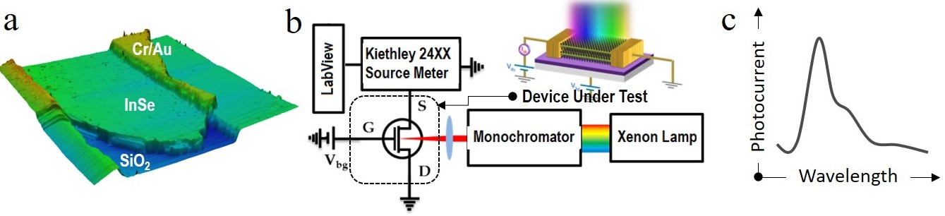
The detail device fabrication method and electrical transport characterization are presented in one of our previous publications WasalaInSe_2020 ; wasala2021-OxfMat . In short the devices were fabricated on Silicon/Silicon dioxide (SiO2) wafers with a (SiO2) thickness of 1000 nm. A typical device fabrication routine involved evaporating metal contacts on top of a suitable flake residing on the Si/SiO2 wafer through shadow masking. We have used either nickel or gold transmission electron microscopy grids for the masking process. After securing TEM grid carefully on top of the flake, system was mounted inside the thermal evaporator chamber. The chamber was then pumped down to 10-6 torr and was held at this pressure overnight. A thin layer of Chromium (Cr) and gold (Au) electrodes were deposited through the mask by evaporating them using a tungsten (W) boat. Typically, about 40 nm of Cr layers and about 160 nm thick Au layer was deposited. After metal deposition, the system was cooled down to room temperature before the devices could be taken out from the metal deposition chamber. The height profile of the device was measured using the contact mode Atomic Force Microscopy (AFM). Height of the device discussed below measured as 34 nm, which is corresponds to 40 InSe layers. Also, active device area was calculated as . The metal contacted flakes were then placed on a ceramic chip holder and gold connecting wires were bonded to the metal contacts using a wire bonder. The chip was then mounted on a closed cycle helium cryostat for with an optical window for desired opto-electronic measurements.
2.3 Photocurrent spectroscopy measurements
Broadband Photo-electronic conduction (PC) characterization was performed using an in house built photocurrent spectroscopy measurement set-up. Xenon lamp was used as a light source to generate broad spectrum of wavelengths (300 nm 1000 nm) and was passed through a Monochromator. These monochromatic light sources were guided on to the device using an optical wave-guide and and focused on to the device using a convex lens with a focal length of 15 cm. Kiethley 2400 series source meters controlled with in-house developed LabVIEW module was utilized for measuring the photo response. Schematic diagram of the experimental setup and typical data obtained is shown in Fig. 1.
3 Results and discussions
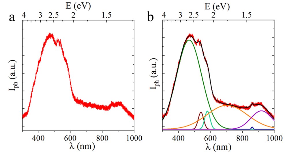
Photocurrent spectroscopy, in the past, have been used widely in order to estimate the broadband optical absorption behavior of a variety of semiconductor material TMDc1982-Kam ; SciRep2D-Klots2014 including, InSeMudd-AdvMat-2013 ; SidongACSNanoInSe , MoS2CommPhys-Vaquero2020 , MoSe22DMater_MoSe2-2017 etc. The generation and/or variation of current as a function of wavelength of light radiation impinging on the material is the core information that can be obtained using this technique. The schematics of our set up and the data obtained using this setup is shown in Fig. 1 and Fig. 2 respectively. The data shown in Fig. 2a, was obtained from a 34 nm thick InSe flake (Fig 1a). From fig. 2a, it is clear that the InSe samples show a broadband photoconductivity, with prominent photoconductivity peaks at several wavelengths. In order to gain insight into the various peaks present in the data, we have have utilized peak fitting with appropriate deconvolution. We found that the peaks from spectra, (Fig. 2a) can be deconvoluted using Eq. 1.
| (1) |
where A is constant, is peak position and is standard deviation. Values of and for all five peaks from Fig. 2b are listed in Table 1.
The general behavior of the photoconductivity as a function of wavelength is presented in figure 2. From figure fig. 2a, it can be seen that the photocurrent slowly increases for decreasing wavelengths close to the bandgap (or E 1.26 eV), and shows a broad peak around 2.5eV. Similar photocurrent peaks are reported for other photoconductive materials in the past JAP-1977-HgI2 ; JAP-Bube-1987-HgI2 ; Burshtein-JAP-1986-HgI2 ; HgI2-BookChapter and can be explained as follows. Initially, the photocurrent increases slowly and then starts to increase sharply from 2 eV till 2.66 eV. This could be generally attributed to increased photon absorption, which leads to an increase in the generated carriers. As the wavelength decreases further the carriers generated increases (at higher energies). The carriers generated at higher energies (lower wavelengths) tends to recombine with surface states, and therefore do not contribute to the photocurrent and hence at lower wavelengths photocurrent decreases sharply (as seen in fig. 2a for E 2.5 eV).
In one of the previous investigations SidongACSNanoInSe related to photocurrent spectroscopy measurement of similar InSe samples (measured within the wavelength of interval 400 nm 800 nm) it was noted that, in case of InSe, electronic transition from Px,y-like orbital to the bottom of conduction band will occur between 2.25 ev (550 nm) and 3.1 eV (400 nm) and electronic transition from Pz-like orbital to the bottom of conduction band will occur between 1.55 eV (800 nm) and 2.25 ev (550 nm) SidongACSNanoInSe . Peaks occurring at similar energy values were observed for our sample as well, as seen from the deconvoluted peaks. We see these similar peaks as indicated in Table 1. For between 800 nm - 1000 nm, a broad shoulder around 900nm (1.4 eV; deconvoluted to two peaks) as seen in figure 2b. Generally, the higher wavelength peaks observed near the band edge are attributed to deep level impurities InSe-Film-1987 , we believe such impurities in our samples are responsible for the peaks observed in the higher wavelength region.
| Peak # | (nm) | E () (eV) | |
|---|---|---|---|
| Peak 1 | 466.56 | 78.09 | 2.658 |
| Peak 2 | 540.40 | 16.77 | 2.296 |
| Peak 3 | 580.79 | 16.55 | 2.134 |
| Peak 4 | 703.68 | 125.89 | 1.772 |
| Peak 5 | 861.10 | 5.26 | 1.439 |
| Peak 6 | 918.94 | 65.53 | 1.349 |
3.1 Band gap determination from photocurrent spectroscopy
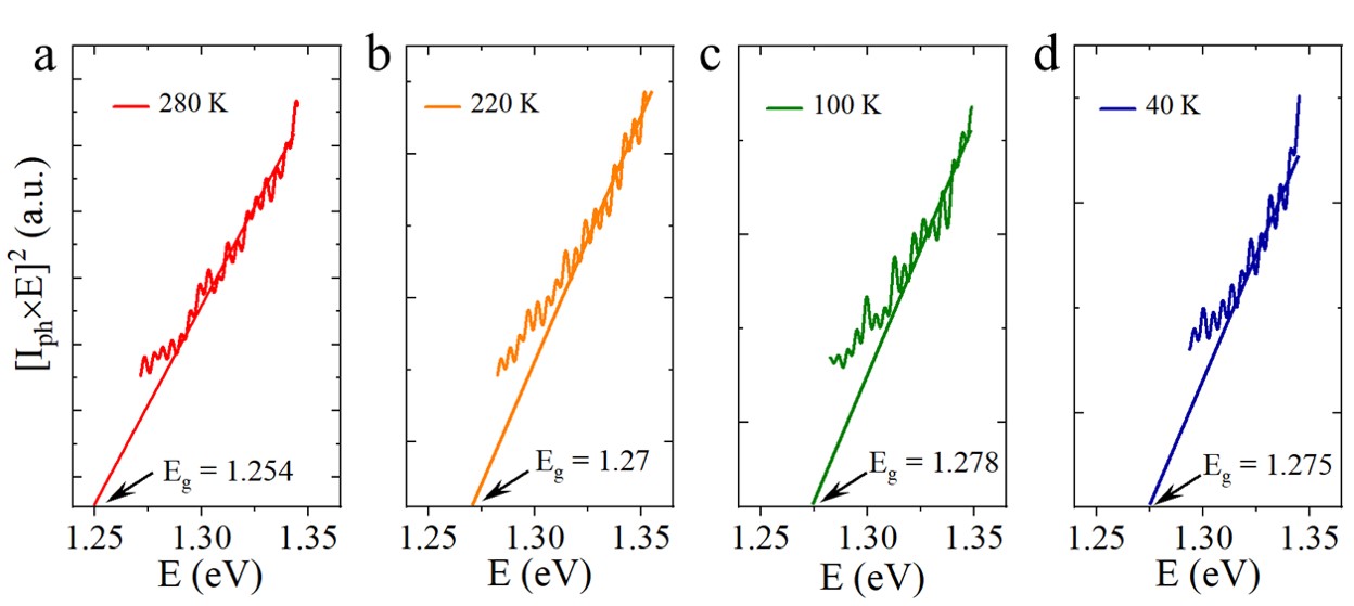
In order to estimate the band gap from photocurrent spectra, we have utilized methods similar to extracting band gap from UV-Vis absorption spectroscopy. Since, the photocurrent generated in a semiconductor is proportional to the number of absorbed photons and the absorption coefficient () of a direct bandgap semiconductor is proportional to the square root of the difference of the photon energy and the bandgap energy, , or in other words . Therefore, it can be assumed that as well and one can generate a plot similar to Tauc plot Tauc-1966 for extracting the band gap values. In the past several investigators have utilized the aforementioned technique and used photocurrent spectroscopy for extraction and estimation of band gap SidongACSNanoInSe ; 2DMater_MoSe2-2017 ; SciRep2D-Klots2014 ; TMDc1982-Kam . For this purpose we have plotted the quantity as a function of as shown in fig 4. For estimation of the band gap from this plot was performed by extrapolating the straight line portion of the data to x-axis intercept. In Fig 4. we have presented such extrapolations for various temperatures. The room temperature band gap value for the measured sample was found to be 1.254eV. This value is similar to the values obtained for multi layered InSe flakes from past investigations InSeTamalampudi ; Mudd-AdvMat-2013 ; InSe-Bandgap-Physica-2014 ; Temp-Bandgap-InSe-2020 .
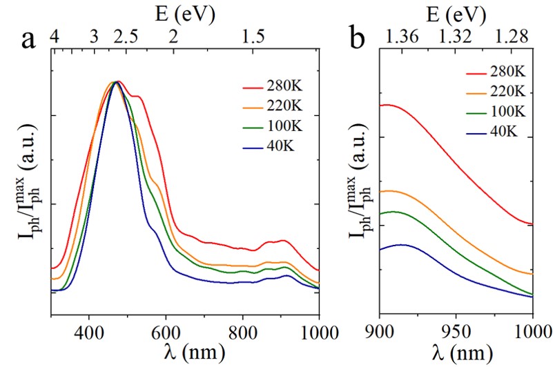
3.2 Temperature dependence of band-gap
Temperature (T) dependence of derived from photocurrent spectroscopy of InSe (Fig. 4) is presented in Fig. 5. The information pertaining to the variation of in semiconductors as a function of temperature is of significance since, such information can be analyzed in order to have fundamental insights about core materials property. Generally, the variation of as a function of T is caused due to the combination of electron-phonon interaction and lattice dilation. In the past, several semi-empirical equations VARSHNI_1967 ; Manoogian-Leclerc_1979 ; Pejova2010Temp ; PhysRevB.86.195208 are developed in order fit the experimental data obtained. One of the most popular approach is to fit the experimental data with Varshani’s equation VARSHNI_1967 , however, it has been argued that in some cases where lattice dilation effects could be significant, a good fit to the experimental data using Varshni equation was not achievable CanJPhys_1984 . Several other equations for example; Bose-Einstein (BE) function Pejova2010Temp , Double Bose-Einstein (DBE) function PhysRevB.86.195208 and Manoogian - Leclerc (ML) Manoogian-Leclerc_1979 equation are also used widely to fit the variation of as a function of T. Below we briefly describe each of these equations and discuss in detail the results obtained by fitting them to our data.
Bose-Einstein function Pejova2010Temp takes into consideration the interaction between electron and phonon and can be represented as shown in Eq. (2).
| (2) |
In this equation, is a band gap at absolute zero (0 K), is a measure of strength of the electron-phonon interaction coupling within the crystal and is the Einstein characteristic temperature. is defined as the average temperature of the phonons which are interacting with the electrons. It is deduced that Debye phonon spectrum with the Debye temperature is equivalent to an Einstein oscillator with a temperature , with Pejova2010Temp . From fitting of Eq. (2) in Fig. 5, a value of is extracted to be 782.2 K. This value of is significantly higher than theoretical value of = 190 K InSeDebyeTempBook as well as experimentally determined maximum possible of 275 K for layered InSe InSeDebye-Tyurin2007 . One reason for such discrepancy could arise from the fact that Bose-Einstein function uses only one Einstein oscillator. In presence of one Einstein oscillator, band-gap energy will either monotonically increase or saturate at constant value as temperature T 0 PhysRevB.86.195208 . For our experimental data, we found a small decrease in ban-gap energy at low temperatures (T 100 K). This behaviour could be elucidate by considering a contribution from low energy (secondary) phonon with opposite weight, leading to decrease in band-gap energy for T 0 PhysRevB.86.195208 . Such contributions can be incorporated by using Double Bose-Einstein function of the form shown in Eq. 3 was used for fitting.
| (3) |
where , , , and have same meaning as previously described. The second Einstein oscillator (third term in Eq. 3 carries a opposite weight to that of the first oscillator. From fitting of Eq. (3) in Fig. 5, a value of is extracted to be 261.3 K, which is much closer to experimentally determined maximum possible Debye temperature of 275 K for layered InSe InSeDebye-Tyurin2007 . The frequencies of the two Bose-Einstein oscillators correspond to optic and acoustic phonons PhysRevB.86.195208 .
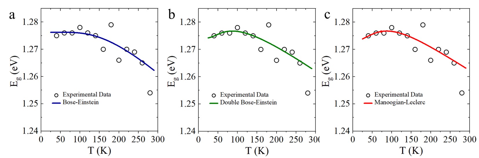
Past investigations have also shown that consideration of lattice dilation effects are crucial in order to explain the temperature variation of band gaps in a variety of semiconductors Manoogian-Leclerc_1979 . In order to determine if there is any lattice dilation effect along with electron-phonon interactions that might influence the variation of with T in our sample, we also considered fitting our data to Manoogian-Leclerc equation, which incorporates the lattice dilation effect term. Eq. 4 shows the form of Manoogian-Leclerc equation.
| (4) |
In Eq. 4, is a band gap at absolute zero (0 K) and U, V, and s are temperature-independent constants. Second and third terms on right hand side of equation correspond to lattice dilation term and electron-phonon interactions respectively. From fitting of Eq. (3) in Fig. 5c, a value of is extracted to be 403.5 K. This value of is substantially higher than experimental values of previously reported for layered InSe InSeDebye-Tyurin2007 . Observing the values obtained specifically from all the fits and comparing it to typical values of reported for layered InSe InSeDebye-Tyurin2007 , we believe that Double Bose-Einstein function is the most closest model that can explain the bandgap shift as a function of temperature observed in our sample. Various parameters obtained from all the fits are summarized in Table 2. From the information presented in Table 2, we note that although the estimated values of for all the models used to fit our experimental data yielded reasonably consistent value of 1.27 eV, this was not the case for values obtained for . One reason for this could be that for a material is often dependent on multiple factors involving the thermodynamic and mechanical properties of material UllrichAIP2017 and hence it becomes extremely difficult to have an accurate and consistent estimation of this value.
| fitting | |||
|---|---|---|---|
| (eV) | (K) | (K) | |
| Bose-Einstein | 1.276 | 588.1 | 782.2 |
| Double Bose-Einstein | 1.274 | 1196.5 | 1261.3 |
| 2180.4 | 2239.9 | ||
| Manoogian-Leclerc | 1.272 | 303.4 | 403.5 |
4 Conclusion
In summary, broadband photoconductive behavior was observed in 34 nm thick flakes of layered InSe. We have tried to investigate the variation of band gap as a function of temperature by performing photocurrent spectroscopy measurements. The data obtained was used to estimate Debye temperature () values of InSe using established theoretical models. The of 260 K obtained using Double Bose-Einstein equation is similar to the values obtained for this quantity for layered InSe. This strongly suggests that Double Bose-Einstein equation is perhaps the best model for explaining the variation of band gap of thin InSe flakes. This would mean (a) that band-gap shifts observed in few layer InSe samples presented in this study depends on electron-phonon interactions, which includes low energy secondary phonons and (b) lattice dilation effects are perhaps negligible in our samples. Most importantly, the variation of the band gap of InSe with temperature presented here is extremely valuable for strengthening our fundamental understanding needed for developing a variety of technological applications using optically active 2D materials.
Acknowledgements.
This work was supported by the U.S. Army Research Office MURI grant #W911NF-11-1-0362. S.T. and P.D.P. acknowledges the support from Indo-U.S. Virtual Networked Joint Center Project on “Light Induced Energy Technologies: Utilizing Promising 2D Nanomaterials (LITE UP 2D)” through the grant number IUSSTF/JC-071/2017. M.W. and P.D.P acknowledges the College of Science Dissertation Research Award and Graduate School Doctoral Fellowship respectively, awarded at Southern Illinois University Carbondale (SIUC).Conflict of interest
The authors declare that they have no conflict of interest.
References
- [1] K. S. Novoselov, A. K. Geim, S. V. Morozov, D. Jiang, Y. Zhang, S. V. Dubonos, I. V. Grigorieva, and A. A. Firsov. Electric field effect in atomically thin carbon films. Science, 306(5696):666–669, 2004.
- [2] Elizabeth Gibney. The super materials that could trump graphene. Nature, 522:274–276, Jun 2015.
- [3] Milinda Wasala, Hansika I Sirikumara, Yub Raj Sapkota, Stephen Hofer, Dipanjan Mazumdar, Thushari Jayasekera, and Saikat Talapatra. Recent advances in investigations of the electronic and optoelectronic properties of group iii, iv, and v selenide based binary layered compounds. Journal of Materials Chemistry C, 5(43):11214–11225, 2017.
- [4] Sujoy Ghosh, Prasanna D Patil, Milinda Wasala, Sidong Lei, Andrew Nolander, Pooplasingam Sivakumar, Robert Vajtai, Pulickel Ajayan, and Saikat Talapatra. Fast photoresponse and high detectivity in copper indium selenide (cuin7se11) phototransistors. 2D Materials, 5(1):015001, oct 2017.
- [5] Prasanna D. Patil, Sujoy Ghosh, Milinda Wasala, Sidong Lei, Robert Vajtai, Pulickel M. Ajayan, Arindam Ghosh, and Saikat Talapatra. Gate-induced metal–insulator transition in 2d van der waals layers of copper indium selenide based field-effect transistors. ACS Nano, 13(11):13413–13420, 2019.
- [6] Prasanna D. Patil, Sujoy Ghosh, Milinda Wasala, Sidong Lei, Robert Vajtai, Pulickel M. Ajayan, and Saikat Talapatra. Electric double layer field-effect transistors using two-dimensional (2d) layers of copper indium selenide (cuin7se11). Electronics, 8(6):645, 2019.
- [7] Sujoy Ghosh, Milinda Wasala, Nihar R Pradhan, Daniel Rhodes, Prasanna D Patil, Michael Fralaide, Yan Xin, Stephen A McGill, Luis Balicas, and Saikat Talapatra. Low temperature photoconductivity of few layer p-type tungsten diselenide (WSe2) field-effect transistors (FETs). Nanotechnology, 29(48):484002, oct 2018.
- [8] Nihar R. Pradhan, Rukshan Thantirige, Prasanna D. Patil, Stephen A. McGill, and Saikat Talapatra. 6 - electronic and optoelectronic properties of the heterostructure devices composed of two-dimensional layered materials. In Satyabrata Jit and Santanu Das, editors, 2D Nanoscale Heterostructured Materials, Micro and Nano Technologies, pages 151–193. Elsevier, 2020.
- [9] Michele Buscema, Joshua O. Island, Dirk J. Groenendijk, Sofya I. Blanter, Gary A. Steele, Herre S. J. van der Zant, and Andres Castellanos-Gomez. Photocurrent generation with two-dimensional van der waals semiconductors. Chem. Soc. Rev., 44:3691–3718, 2015.
- [10] Hehai Fang and Weida Hu. Photogating in low dimensional photodetectors. Advanced Science, 4(12):1700323, 2017.
- [11] Melinda Mohl, Anne-Riikka Rautio, Georgies Alene Asres, Milinda Wasala, Prasanna Dnyaneshwar Patil, Saikat Talapatra, and Krisztian Kordas. 2d tungsten chalcogenides: Synthesis, properties and applications. Advanced Materials Interfaces, 7(13):2000002, 2020.
- [12] Song-Lin Li, Kazuhito Tsukagoshi, Emanuele Orgiu, and Paolo Samorì. Charge transport and mobility engineering in two-dimensional transition metal chalcogenide semiconductors. Chem. Soc. Rev., 45:118–151, 2016.
- [13] Oriol Lopez-Sanchez, Dominik Lembke, Metin Kayci, Aleksandra Radenovic, and Andras Kis. Ultrasensitive photodetectors based on monolayer mos2. Nature Nanotechnology, 8(7):497–501, Jul 2013.
- [14] Néstor Perea-López, Ana Laura Elías, Ayse Berkdemir, Andres Castro-Beltran, Humberto R. Gutiérrez, Simin Feng, Ruitao Lv, Takuya Hayashi, Florentino López-Urías, Sujoy Ghosh, Baleeswaraiah Muchharla, Saikat Talapatra, Humberto Terrones, and Mauricio Terrones. Photosensor device based on few-layered ws2 films. Advanced Functional Materials, 23(44):5511–5517, 2013.
- [15] Dominik Kufer and Gerasimos Konstantatos. Photo-fets: Phototransistors enabled by 2d and 0d nanomaterials. ACS Photonics, 3(12):2197–2210, 2016.
- [16] Srinivasa Reddy Tamalampudi, Yi-Ying Lu, Rajesh Kumar U., Raman Sankar, Chun-Da Liao, Karukanara Moorthy B., Che-Hsuan Cheng, Fang Cheng Chou, and Yit-Tsong Chen. High performance and bendable few-layered inse photodetectors with broad spectral response. Nano Letters, 14(5):2800–2806, 2014. PMID: 24742243.
- [17] Garry W. Mudd, Simon A. Svatek, Tianhang Ren, Amalia Patanè, Oleg Makarovsky, Laurence Eaves, Peter H. Beton, Zakhar D. Kovalyuk, George V. Lashkarev, Zakhar R. Kudrynskyi, and Alexandr I. Dmitriev. Tuning the bandgap of exfoliated inse nanosheets by quantum confinement. Advanced Materials, 25(40):5714–5718, 2013.
- [18] Sidong Lei, Liehui Ge, Sina Najmaei, Antony George, Rajesh Kappera, Jun Lou, Manish Chhowalla, Hisato Yamaguchi, Gautam Gupta, Robert Vajtai, Aditya D. Mohite, and Pulickel M. Ajayan. Evolution of the electronic band structure and efficient photo-detection in atomic layers of inse. ACS Nano, 8(2):1263–1272, 2014. PMID: 24392873.
- [19] Biljana Pejova, Bahattin Abay, and Irina Bineva. Temperature dependence of the band-gap energy and sub-band-gap absorption tails in strongly quantized znse nanocrystals deposited as thin films. The Journal of Physical Chemistry C, 114(36):15280–15291, 2010.
- [20] J. Bhosale, A. K. Ramdas, A. Burger, A. Muñoz, A. H. Romero, M. Cardona, R. Lauck, and R. K. Kremer. Temperature dependence of band gaps in semiconductors: Electron-phonon interaction. Phys. Rev. B, 86:195208, Nov 2012.
- [21] A. Manoogian and A. Leclerc. Determination of the dilation and vibrational contributions to the energy band gaps in germanium and silicon. physica status solidi (b), 92(1):K23–K27, 1979.
- [22] Milinda Wasala, Prasanna D Patil, Sujoy Ghosh, Rana Alkhaldi, Lincoln Weber, Sidong Lei, Robert Vajtai, Pulickel M Ajayan, and Saikat Talapatra. Influence of channel thickness on charge transport behavior of multi-layer indium selenide (InSe) field-effect transistors. 2D Materials, 7(2):025030, feb 2020.
- [23] Milinda Wasala, Prasanna D. Patil, Sujoy Ghosh, Lincoln Weber, Sidong Lei, and Saikat Talapatra. Role of layer thickness and field-effect mobility on photoresponsivity of indium selenide (inse) based phototransistors, 2021.
- [24] K. K. Kam and B. A. Parkinson. Detailed photocurrent spectroscopy of the semiconducting group vib transition metal dichalcogenides. The Journal of Physical Chemistry, 86(4):463–467, 1982.
- [25] A. R. Klots, A. K. M. Newaz, Bin Wang, D. Prasai, H. Krzyzanowska, Junhao Lin, D. Caudel, N. J. Ghimire, J. Yan, B. L. Ivanov, K. A. Velizhanin, A. Burger, D. G. Mandrus, N. H. Tolk, S. T. Pantelides, and K. I. Bolotin. Probing excitonic states in suspended two-dimensional semiconductors by photocurrent spectroscopy. Scientific Reports, 4(1):6608, Oct 2014.
- [26] Daniel Vaquero, Vito Clericò, Juan Salvador-Sánchez, Adrián Martín-Ramos, Elena Díaz, Francisco Domínguez-Adame, Yahya M. Meziani, Enrique Diez, and Jorge Quereda. Excitons, trions and rydberg states in monolayer mos2 revealed by low-temperature photocurrent spectroscopy. Communications Physics, 3(1):194, Oct 2020.
- [27] Jorge Quereda, Talieh S Ghiasi, Feitze A van Zwol, Caspar H van der Wal, and Bart J van Wees. Observation of bright and dark exciton transitions in monolayer MoSe2 by photocurrent spectroscopy. 2D Materials, 5(1):015004, oct 2017.
- [28] F. Adduci, A. Cingolani, M. Ferrara, M. Lugarà, and A. Minafra. Photoelectromagnetic properties of hgi2. Journal of Applied Physics, 48(1):342–345, 1977.
- [29] Jonathan Bornstein and Richard H. Bube. Photoelectronic properties of hgi2. Journal of Applied Physics, 61(7):2676–2678, 1987.
- [30] Z. Burshtein, Justin K. Akujieze, and E. Silberman. Carrier surface generation and recombination effects in photoconduction of hgi2 single crystals. Journal of Applied Physics, 60(9):3182–3187, 1986.
- [31] X.J. Bao, T.E. Schlesinger, and R.B. James. Chapter 4 - electrical properties of mercuric iodide. In T.E. Schlesinger and Ralph B. James, editors, Semiconductors and Semimetals, volume 43 of Semiconductors and Semimetals, pages 111–168. Elsevier, 1995.
- [32] M. Yudasaka, T. Matsuoka, and K. Nakanishi. Indium selenide film formation by the double-source evaporation of indium and selenium. Thin Solid Films, 146(1):65–73, 1987.
- [33] J. Tauc, R. Grigorovici, and A. Vancu. Optical properties and electronic structure of amorphous germanium. physica status solidi (b), 15(2):627–637, 1966.
- [34] Bekir Gürbulak, Mehmet Şata, Seydi Dogan, Songul Duman, Afsoun Ashkhasi, and E. Fahri Keskenler. Structural characterizations and optical properties of inse and inse:ag semiconductors grown by bridgman/stockbarger technique. Physica E: Low-dimensional Systems and Nanostructures, 64:106–111, 2014.
- [35] M. Isik and N.M. Gasanly. Temperature-tuned band gap characteristics of inse layered semiconductor single crystals. Materials Science in Semiconductor Processing, 107:104862, 2020.
- [36] Y.P. Varshni. Temperature dependence of the energy gap in semiconductors. Physica, 34(1):149–154, 1967.
- [37] A. Manoogian and J. C. Woolley. Temperature dependence of the energy gap in semiconductors. Canadian Journal of Physics, 62(3):285–287, 1984.
- [38] O. Madelung, U. Rössler, and M. Schulz. Indium selenide (inse) debye temperature, heat capacity, density, melting point: Datasheet from landolt-börnstein - group iii condensed matter · volume 41c: “non-tetrahedrally bonded elements and binary compounds i” in springermaterials (https://doi.org/10.1007/10681727_514).
- [39] A. V. Tyurin, K. S. Gavrichev, and V. P. Zlomanov. Low-temperature heat capacity and thermodynamic properties of inse. Inorganic Materials, 43(9):921–925, Sep 2007.
- [40] Bruno Ullrich, Mithun Bhowmick, and Haowen Xi. Relation between debye temperature and energy band gap of semiconductors. AIP Advances, 7(4):045109, 2017.