Electrically driven linear optical isolation through phonon mediated Autler-Townes splitting
Abstract
Optical isolators are indispensible components in nearly all photonic systems as they help ensure unidirectionality and provide crucial protection from undesirable reflections. While commercial isolators are exclusively built on magneto-optic (MO) principles they are not readily implemented within photonic integrated circuits due to the need for specialized materials. Importantly, the MO effect is generally weak, especially at shorter wavelengths. These challenges as a whole have motivated extensive research on non-MO alternatives [Hwang:97, KangM.2011, Doerr:11, lira2012, Tzuang2014, 10, Sounas:14, Dong2015, Kim2015, Kim2016, Ruesink:16, Fang:2017, Sohn18, Kittlaus2018, Peterson:18, 18, 2, 20, 17, 4, 8, 9]. To date, however, no alternative technology has managed to simultaneously combine linearity (i.e. no frequency shift), linear response (i.e. input-output scaling), ultralow insertion loss, and large directional contrast on-chip. Here we demonstrate an optical isolator design that leverages the unbeatable transparency of a short, high quality dielectric waveguide, with the near-perfect attenuation from a critically-coupled absorber. Our design concept is implemented using a lithium niobate racetrack resonator in which phonon mediated [Sohn18] Autler-Townes splitting (ATS) [14, Kim2016, 18, 23] breaks the chiral symmetry of the resonant modes. We demonstrate on-chip optical isolators at wavelengths one octave apart near 1550 nm and 780 nm, fabricated from the same lithium niobate-on-insulator wafer. Linear optical isolation is demonstrated with simultaneously 1 dB insertion loss, 39 dB contrast, and bandwidth as wide as the optical mode that is used. Our results outperform the current best-in-class MO isolator on-chip on both insertion loss and isolator figures-of-merit, and demonstrate a lithographically defined wavelength adaptability that cannot yet be achieved with any MO isolator.
Magneto-optic (MO) isolators, based on asymmetric Faraday rotation, have long dominated nonreciprocal photonic device technologies as they simultaneously provide low insertion loss, high directional contrast, and wide bandwidth. While a number of attempts have been made to bring these devices on chip [Ross:11, 6, Huang:17, 22, 5, Zhang:19, 21], with some measure of success, there remain many unresolved challenges that have held back full adoption. The foremost among these is the lack of appropriate materials in photonics foundries, and the additional technical constraint of magnetic biasing. Recent results [21, Zhang:19, 22] on integrated magneto-optic isolators have been successful at achieving low insertion loss over modest bandwidth, however they cannot easily be adapted to any wavelength of choice since the Faraday effect is chromatic, i.e. is a strong function of the wavelength. Moreover, the MO material stack is intrinsically lossy and therefore the best current examples [21, Zhang:19, 22] attempt to use the minimum possible amount of MO material.
Due to a wide recognition of these limitations, extensive research has been performed on alternative isolator and circulator technologies that leverage synthetic fields [Tzuang2014, 10, Fang:2017, 8], optomechanics [KangM.2011, Sounas:14, Kim2015, Dong2015, Kim2016, Ruesink:16], acousto-optics [Sohn18, 2, Kittlaus2018, 9, Hwang:97, 20, 17], electro-optics [Doerr:11, lira2012, 18, 4], spinning resonators [12], and chirally pumped atoms [Scheucher:16]. These techniques may be generally considered as variations on spatio-temporal modulation and use some momentum conservation rule or momentum bias to break reciprocity. Often these approaches operate over a narrow bandwidth, which is quite acceptable for a wide variety of single-frequency laser applications, for instance in ultra-stable sources [19, 11], LIDAR [15], frequency combs [3], and atomic referencing [7, Knappe:04, 13]. A number of these alternative techniques have demonstrated very large optical contrast [4] (see also Supplement §S7), but ultimately the ability to provide low insertion loss remains a huge technical challenge.
The absolute ideal for a two-port low loss device on chip is simply a high quality linear waveguide of short length. This represents the best case for achieving the lowest forward insertion loss in the ‘high transparency’ direction of an isolator. We now introduce a narrow-band absorber, e.g. a high-Q resonator, that is shunt-coupled to this ideal waveguide [Peterson:18, Kim2016]. If this absorber is detuned more than a few linewidths from the frequency of interest, it will not be accessible to light propagating within the waveguide and a high transparency is observed (Fig. 1a). On the other hand, when light is on resonance with the absorber, and if the absorber is critically coupled to the waveguide (Fig. 1b), then a giant attenuation factor can be achieved. Here, critical coupling occurs when the intrinsic loss rate for the WGR mode is matched to the coupling rate from the external interface (Supplement §S2). It is this combination of near-ideal transparency and giant attenuation that we wish to simultaneously exploit [Kim2016, 18], and it can be achieved using a narrow-band absorber with broken chiral symmetry (Fig. 1c).
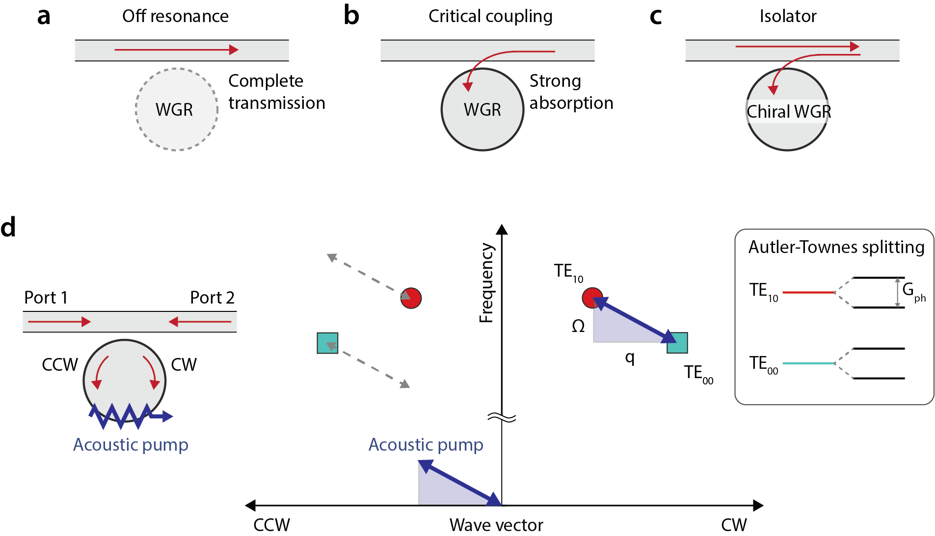
In this Letter we report on a method to induce very large chiral asymmetry in a two-level photonic atom using phonon mediated Autler-Townes splitting (ATS) [Kim2016, 18, Sohn18]. When coupled with a waveguide, the resulting isolator exhibits near ideal characteristics. The two-level photonic atom is produced using a whispering gallery racetrack resonator (WGR) that supports two families of optical modes belonging to TE10 and TE00 families. We identify a mode pair that is closely spaced in frequency near a mode family crossing, with the TE00 mode () and TE10 mode () having distinct frequencies and wavevectors as shown in Fig. 1d. These two modes can be unidirectionally coupled through acousto-optic scattering, as long as the difference of frequency () and momentum () between the optical modes matches the frequency and momentum of an acoustic excitation of the material. In addition, the overlap integral between the acoustic mode and optical modes must be non-zero [Sohn18]. Both these requirements, while tricky, can be simultaneously achieved by the engineering of a 2D ‘texture’ for the acoustic excitation of the resonator [Sohn18, 2], such that there is a non-zero momentum along the WGR circuit, while a standing wave exists in the transverse direction. When the phonon-enhanced optomechanical coupling rate () exceeds the optical loss rates () we enter the strong coupling or ATS regime (see Supplement §S1). This regime manifests as a unidirectional hybridization of the selected TE10 and TE00 modes, modifying their dispersion and frequency-splitting the resonant absorption in the phase matched direction only. In this analogy, the determines the amount of frequency splitting and is equivalent to the Rabi frequency in atomic ATS. In this situation, light propagating at the original optical resonance frequencies ( and ) in the waveguide no longer interacts with the resonator and simply propagates through. This will be the case as long as the process is reasonably well phase matched, and the coupling rate is sufficiently large. In the non-phase matched direction, however, the original optical modes remain unmodified. As a result, if we can design the system to achieve critical coupling for the TE10 mode, then giant contrast is simultaneously achieved (see Supplement §S2). As a result of this architecture our approach achieves unidirectional strong coupling and large nonreciprocity with a single RF input, without requiring multiple phase-shifted signals, which is common in other spatiotemporal modulation approaches.
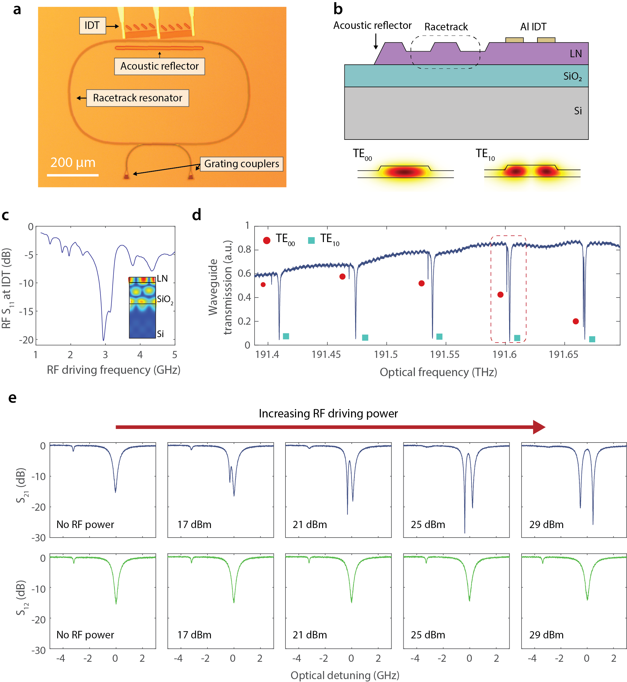
For experimental implementation, we used a lithium niobate-on-insulator (LNOI) integrated photonics platform. The wide bandgap of lithium niobate (LN) imparts a broad transparency window spanning 250 nm to 5300 nm. Additionally, the high piezoelectric coefficient in LN allows very efficient actuation of surface acoustic waves via RF stimulus [1], which is a specific advantage for this device. In contrast to previous efforts that used aluminum nitride as the photonic and piezoelectric material [2, Sohn18], here we are able achieve much higher optical Q-factors ( at 780 nm, at 1550 nm) and significantly better electromechanical transduction efficiency (about 10x higher at ). The two-mode racetrack resonators and adjacent single-mode waveguides (Fig. 2a) are etched with ridge waveguide geometry (see Supplement §S5). Grating couplers covering the wavelength range of interest are fabricated on either end of the waveguide to provide off-chip optical access to the isolator. Finally, to ensure the transverse standing wave characteristic for the acoustic excitation, we fabricate an acoustic reflector by fully etching the LN thin film on the far side of the racetrack (Fig. 2a,b).
We first characterize the primary acoustic and optical components of the isolator. Measurement of the RF reflection coefficient (S11) of the IDT shows a dip near 3 GHz, confirming excitation of the surface acoustic wave (Fig. 2c). The optical states of the racetrack resonator are measured by probing transmission through the adjacent waveguide. As seen in Fig. 2d, two optical mode families can be identified, with the TE10 family better coupled to the waveguide due to its larger evanescent field. In fact, the TE10 mode is critically coupled to the waveguide to ensure maximum attenuation in the backward direction. The TE00 mode is kept intentionally dark (i.e. under-coupled) since it is helpful to both lower the requirement and, as we discuss later, to suppress sideband generation. The device is designed such that there is a mode crossing near the wavelength of interest. For the specific device shown, we find an optical mode pair located near 192.6 THz (1556 nm) that has a frequency separation of GHz, which is similar to the acoustic frequency. Finally, a constant RF tone at 3 GHz is applied to the IDT, which launches the 2D surface acoustic wave and hybridizes the two optical modes producing the ATS.
We experimentally measure the non-reciprocal transmission using optical heterodyne detection (see Supplement §S6) which enables separate measurement of the carrier signal transmission and its sidebands. Fig. 2e shows the evolution of the optical spectrum for increasing RF driving power, in both forward and backward directions through the waveguide ports. We define the frequency of the original TE10 mode as the zero detuning point. In the phase matched direction (forward), the optical modes experience a clear ATS phenomenon, with the central transmission at zero detuning approaching unity for large drive power. At the same time, the optical modes remain unperturbed in the non-phase matched direction (backward).
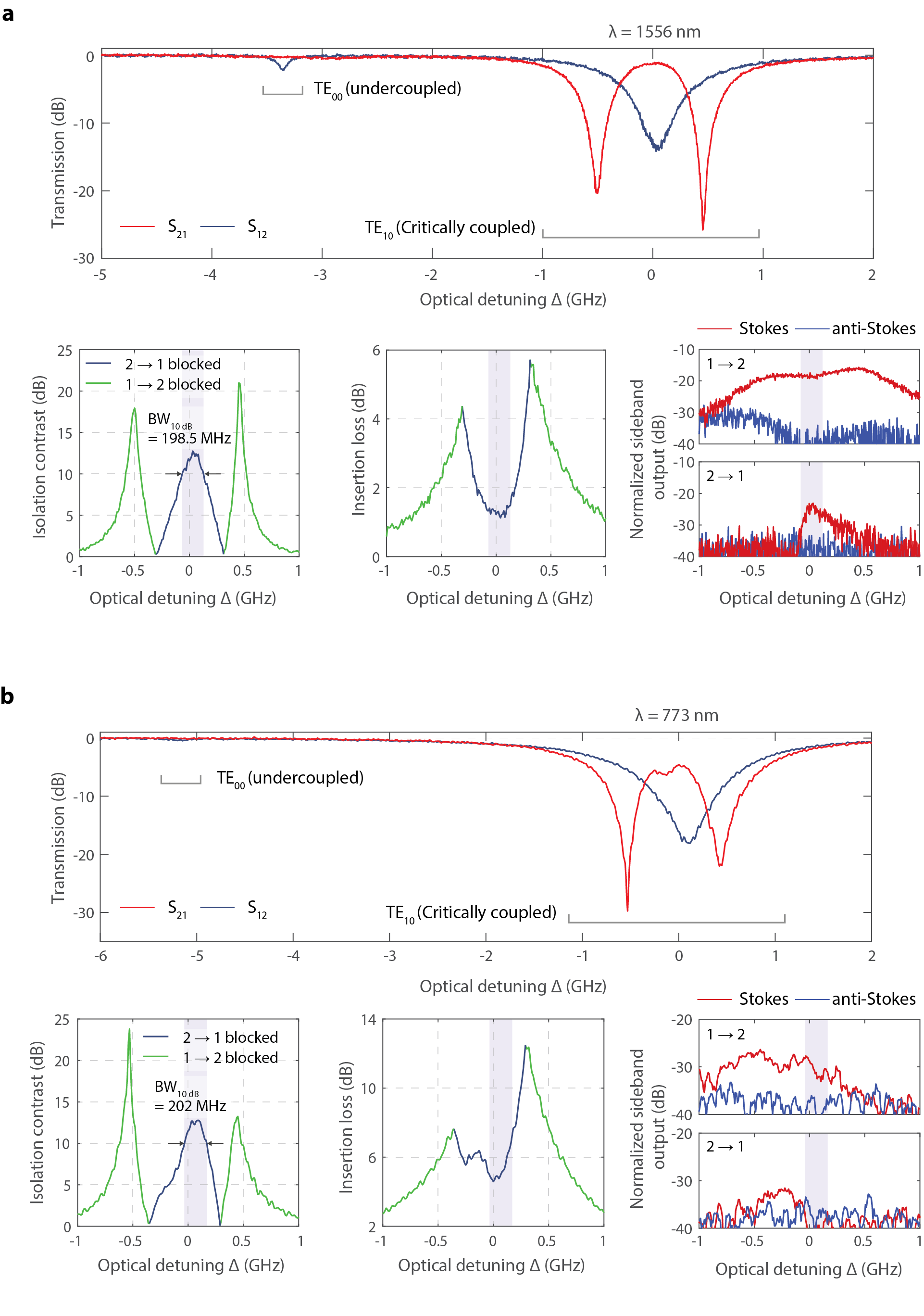
A closer examination of the telecom (1550 nm) wavelength isolator is presented in Fig. 3a. We observe that this device simultaneously achieves 1.13 dB forward insertion loss with 12.75 dB peak contrast using 29 dBm of RF driving power. This drive level corresponds to a phonon-enhanced optomechanical coupling rate of 0.98 GHz, and we are currently prevented from increasing this further due to the power handling capability of the IDTs. The nonreciprocal contrast here is limited only by the degree to which we are able to approach the critical coupling in the fabricated device. While our main attention is on the central isolation behavior, we also observe appreciable nonreciprocity on the the wings corresponding to the dressed states, although here we must reverse the description of forward and backward propagation (as those are arbitrary definitions). During the experiment, we are also able to monitor the GHz sidebands of the carrier signal, and we find that they are consistently dB below (or more) the original carrier signal power. This is thanks to a combination of the very high which significantly reduces interaction between the waveguide and WGR at , and also thanks to the undercoupled TE00 mode which does not couple well to the waveguide. Further discussion is provided in the Supplement §S3.
Since all features of this device are lithographically defined, and do not depend on any wavelength-dependent material gyrotropic property (e.g. the Faraday rotation effect in magneto-optics), we are able to shift the operational wavelength of this isolator freely within the transparency range of lithium niobate. In fact, the optomechanical coupling is directly proportional to the optical frequency, implying that isolators operating at short wavelengths with comparable parameters will require lower power. There is, however, the possibility that this advantage is offset by the generally higher surface scattering induced loss at short wavelengths. In this context, we developed a 780 nm demonstration (Fig. 3b) for the isolator using the same LNOI substrate. This device simultaneously achieves 4.76 dB forward insertion loss with 12.86 dB peak contrast, using 25 dBm of RF driving power to reach GHz. While the insertion loss achieved in this device was not as low, the sideband generation is significantly reduced since the TE00 mode is almost completely dark.
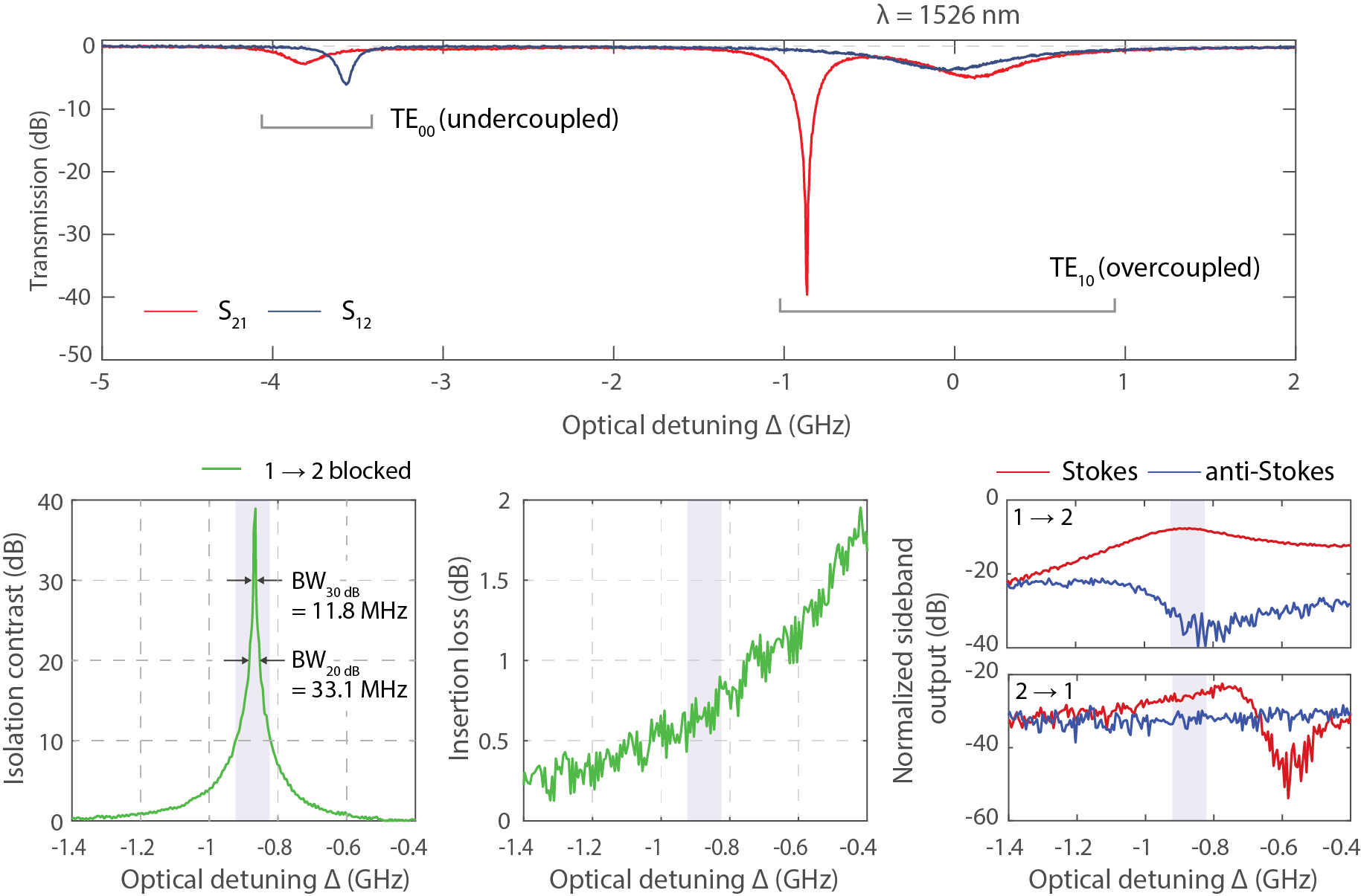
In the above ATS-based approach, the isolation contrast is primarily dictated by the criticality of coupling between the waveguide and the optical mode (here, the TE10 mode) and is therefore strongly dependent on the fabricated geometry. Contrast factors greater than 25 dB can therefore be difficult to achieve because of the matching requirement with the intrinsic resonator loss. One solution to the contrast problem is to instead leverage the nonreciprocal wings to either side of the central nonreciprocal band. In these bands, the contrast is dictated by the placement of, and coupling to the dressed states. The contrast is therefore a function of , and of the relative mismatch between the optical mode separation and the applied phonon frequency. Additional discussion of this situation is provided in the Supplement §S4. As a key result, we find that if the TE10 mode is intentionally overcoupled, and the mode mismatch is , then there exists a choice of where critical coupling is achievable near the lower dressed state. Conversely, for the critical coupling is achievable near the upper dressed state. A dramatic example of this situation is presented for an overcoupled 1538 nm isolator in Fig. 4, where on the lower dressed state we can simultaneously observe dB insertion loss with dB contrast, using 29 dBm of RF driving power to reach GHz. Here, the spacing between the optical modes is 3.72 GHz while the RF drive is at 3 GHz, implying a GHz. We also implemented this effect with opposite using a device operating near 780 nm (see Supplementary Fig. S4).
We can understand this phenomenon fairly intuitively by considering instead a sideband picture, which works since the mismatch puts the system in a regime between pure ATS and the ac Stark effect (the latter explains the noticeable frequency shifts of the modes). As we scan the overcoupled TE10 mode (i.e. intrinsic loss rate extrinsic coupling rate), we find a range of frequencies where the scattering into the nearly dark TE10 is resonantly enhanced. This implies that as increases, the effective intrinsic loss rate of the TE10 mode over this band increases, and can approach the extrinsic coupling rate to hit criticality. This intuitive explanation is also experimentally supported by the increased Stokes sideband power in the case in Fig. 4 which indicates increased scattering into the TE00 mode. While this approach is much more sensitive to the value of , unlike the central isolation band, the tunability of this operation regime can be advantageous and ultimately delivers better results in the devices shown in this paper.
Since isolators are often used in cascaded configurations, citing insertion loss (IL) or isolation contrast (IC) alone is not meaningful. Instead, as discussed previously [Kim2016], the ratio of IC per dB of IL is the relevant figure of merit (FoM) that accounts for cascading. We find that this device (Fig. 4) not only provides IC at par with the best magneto-optic isolators, but significantly outperforms them on IL and the isolator FoM (comparison in Supplement §S7). The main disadvantage of our approach compared to magneto-optics is the narrower operational bandwidth, but this could be addressed in the future with designs that achieve higher .
The lack of optical isolators in photonic integrated circuits has long been a technological hurdle, and their absence is uniquely felt by contemporary quantum and atomic microsystems. Isolator and circulator banks are extensively used in low-temperature quantum technologies to suppress thermal noise, but stray magnetic fields from available isolators can be problematic for superconducting materials, e.g. in qubits. Magnetless isolators at visible and near-IR wavelengths are also critically needed to enable chip scale atom-photon integration [Knappe:04, 7, 16], as they can circumvent undesirable Zeeman shifts [Blanshan:05]. The isolators that we have demonstrated are extremely well-positioned to address these applications, as they exhibit narrowband performance at par with current off-chip magneto-optic isolators, while at the same time providing access to wavelength ranges that are challenging with magneto-optic techniques.
References
- [1] Cited by: Electrically driven linear optical isolation through phonon mediated Autler-Townes splitting.
- [2] (2019/12/01) Direction reconfigurable nonreciprocal acousto-optic modulator on chip. APL Photonics 4 (12), pp. 126103. Note: doi: 10.1063/1.5123497 External Links: Document Cited by: Figure 2, Electrically driven linear optical isolation through phonon mediated Autler-Townes splitting, Electrically driven linear optical isolation through phonon mediated Autler-Townes splitting, Electrically driven linear optical isolation through phonon mediated Autler-Townes splitting, Electrically driven linear optical isolation through phonon mediated Autler-Townes splitting.
- [3] (2007) Optical frequency comb generation from a monolithic microresonator. Nature 450 (7173), pp. 1214–1217. External Links: Document, ISBN 1476-4687 Cited by: Electrically driven linear optical isolation through phonon mediated Autler-Townes splitting.
- [4] (2021) Optical isolation using microring modulators. Optics Letters 46 (3), pp. 460–463. External Links: Document Cited by: Electrically driven linear optical isolation through phonon mediated Autler-Townes splitting, Electrically driven linear optical isolation through phonon mediated Autler-Townes splitting.
- [5] (2018/12/19) Monolithic on-chip magneto-optical isolator with 3 dB insertion loss and 40 db isolation ratio. ACS Photonics 5 (12), pp. 5010–5016. Note: doi: 10.1021/acsphotonics.8b01257 External Links: Document Cited by: Electrically driven linear optical isolation through phonon mediated Autler-Townes splitting.
- [6] (2012-01) Ce:YIG/Silicon-on-insulator waveguide optical isolator realized by adhesive bonding. Opt. Express 20 (2), pp. 1839–1848. External Links: Document Cited by: Electrically driven linear optical isolation through phonon mediated Autler-Townes splitting.
- [7] (2018) Photonic chip for laser stabilization to an atomic vapor with 10 instability. Optica 5 (4), pp. 443–449. External Links: Document Cited by: Electrically driven linear optical isolation through phonon mediated Autler-Townes splitting, Electrically driven linear optical isolation through phonon mediated Autler-Townes splitting.
- [8] (2021/01/01) On-chip optical non-reciprocity through a synthetic hall effect for photons. APL Photonics 6 (1), pp. 011301. Note: doi: 10.1063/5.0034291 External Links: Document Cited by: Electrically driven linear optical isolation through phonon mediated Autler-Townes splitting, Electrically driven linear optical isolation through phonon mediated Autler-Townes splitting.
- [9] (2021) Electrically driven acousto-optics and broadband non-reciprocity in silicon photonics. Nature Photonics 15 (1), pp. 43–52. External Links: Document, ISBN 1749-4893 Cited by: Electrically driven linear optical isolation through phonon mediated Autler-Townes splitting, Electrically driven linear optical isolation through phonon mediated Autler-Townes splitting.
- [10] (2014) Photonic aharonov–bohm effect in photon–phonon interactions. Nature Communications 5 (1), pp. 3225. External Links: Document, ISBN 2041-1723 Cited by: Electrically driven linear optical isolation through phonon mediated Autler-Townes splitting, Electrically driven linear optical isolation through phonon mediated Autler-Townes splitting.
- [11] (2020) Ultralow-noise photonic microwave synthesis using a soliton microcomb-based transfer oscillator. Nature Communications 11 (1), pp. 374. External Links: Document, ISBN 2041-1723 Cited by: Electrically driven linear optical isolation through phonon mediated Autler-Townes splitting.
- [12] (2018) Flying couplers above spinning resonators generate irreversible refraction. Nature 558 (7711), pp. 569–572. External Links: Document, ISBN 1476-4687 Cited by: Electrically driven linear optical isolation through phonon mediated Autler-Townes splitting.
- [13] (2019) Architecture for the photonic integration of an optical atomic clock. Optica 6 (5), pp. 680–685. External Links: Document Cited by: Electrically driven linear optical isolation through phonon mediated Autler-Townes splitting.
- [14] (2014) What is and what is not electromagnetically induced transparency in whispering-gallery microcavities. Nature Communications 5 (1), pp. 5082. External Links: Document, ISBN 2041-1723 Cited by: Electrically driven linear optical isolation through phonon mediated Autler-Townes splitting.
- [15] (2017) Coherent solid-state lidar with silicon photonic optical phased arrays. Optics Letters 42 (20), pp. 4091–4094. External Links: Document Cited by: Electrically driven linear optical isolation through phonon mediated Autler-Townes splitting.
- [16] (2010) Atom-chip-based generation of entanglement for quantum metrology. Nature 464 (7292), pp. 1170–1173. External Links: ISBN 1476-4687 Cited by: Electrically driven linear optical isolation through phonon mediated Autler-Townes splitting.
- [17] (2020) Acousto-optic modulation of a wavelength-scale waveguide. arXiv:2010.12517. Cited by: Electrically driven linear optical isolation through phonon mediated Autler-Townes splitting, Electrically driven linear optical isolation through phonon mediated Autler-Townes splitting.
- [18] (2018) Nonreciprocal optical dissipation based on direction-dependent rabi splitting. IEEE Journal of Selected Topics in Quantum Electronics 24 (6), pp. 1–7. External Links: Document, ISBN 1558-4542 Cited by: Electrically driven linear optical isolation through phonon mediated Autler-Townes splitting, Electrically driven linear optical isolation through phonon mediated Autler-Townes splitting, Electrically driven linear optical isolation through phonon mediated Autler-Townes splitting, Electrically driven linear optical isolation through phonon mediated Autler-Townes splitting.
- [19] (2018) An optical-frequency synthesizer using integrated photonics. Nature 557 (7703), pp. 81–85. External Links: Document, ISBN 1476-4687 Cited by: Electrically driven linear optical isolation through phonon mediated Autler-Townes splitting.
- [20] (2020) Hybrid integrated photonics using bulk acoustic resonators. Nature Communications 11 (1), pp. 3073. External Links: Document, ISBN 2041-1723 Cited by: Electrically driven linear optical isolation through phonon mediated Autler-Townes splitting, Electrically driven linear optical isolation through phonon mediated Autler-Townes splitting.
- [21] (2020-11) Waveguide-integrated high-performance magneto-optical isolators and circulators on silicon nitride platforms. Optica 7 (11), pp. 1555–1562. External Links: Document Cited by: Electrically driven linear optical isolation through phonon mediated Autler-Townes splitting.
- [22] (2017) Monolithically-integrated TE-mode 1D silicon-on-insulator isolators using seedlayer-free garnet. Scientific Reports 7 (1), pp. 5820. External Links: Document, ISBN 2045-2322 Cited by: Electrically driven linear optical isolation through phonon mediated Autler-Townes splitting.
- [23] (2019) Electronically programmable photonic molecule. Nature Photonics 13 (1), pp. 36–40. External Links: Document, ISBN 1749-4893 Cited by: Electrically driven linear optical isolation through phonon mediated Autler-Townes splitting.
Acknowledgments
This work was sponsored by the Defense Advanced Research Projects Agency (DARPA) grant FA8650-19-2-7924, the National Science Foundation EFRI grant EFMA-1641084, and the Air Force Office of Scientific Research (AFOSR) grant FA9550-19-1-0256. GB would additionally like to acknowledge support from the Office of Naval Research (ONR) Director for Research Early Career grant N00014-17-1-2209, and the Presidential Early Career Award for Scientists and Engineers. DBS would also like to acknowledge support from a US National Science Foundation Graduate Research Fellowship. The US Government is authorized to reproduce and distribute reprints for Governmental purposes notwithstanding any copyright notation thereon. The views and conclusions contained herein are those of the authors and should not be interpreted as necessarily representing the official policies or endorsements, either expressed or implied, of DARPA or the U.S. Government.
Data availability
The data that support the findings of this study are available from the corresponding author upon reasonable request.
Supplementary Information:
Electrically driven linear optical isolation through phonon mediated Autler-Townes splitting
Donggyu B. Sohn†,
Oğulcan E. Örsel†,
and Gaurav Bahl
Department of Mechanical Science and Engineering,
University of Illinois at Urbana–Champaign, Urbana, IL 61801 USA,
These authors contributed equally
S1 Analytical description of phonon mediated ATS
Here we present a mathematical discussion of the phonon mediated ATS process by invoking the analysis previously performed in [1]. The coupled equations of motion for the optical fields in the WGR and waveguide (see Fig. S1) can be expressed in matrix form:
| (S1) |
where () is the intracavity field for the TE00 (TE10) mode, () is the loaded decay rate, () is the external coupling rate, () is the resonant frequency, is the acousto-optic coupling rate, is the RF driving frequency, is the input laser frequency, and is the input field in the waveguide.
In our case, the TE00 mode is intentionally undercoupled relative to the waveguide in order to minimize the sidebands as discussed below in §S3. Thus, we can neglect the external coupling rate of TE00 mode (set ). We can define an additional subscript for the field terms to indicate the original carrier frequency, to indicate the first order upper sideband, and to indicate the first order lower sideband respectively. Presently, we are interested in the optical output at the input (carrier) frequency (ignoring the sidebands ) from the waveguide using the expression:
| (S2) |
where the TE10 intracavity field at the input frequency () can be expressed as:
| (S3) |
where is the optical detuning from the TE10 mode and is the frequency mismatch between the optical mode separation and the applied phonon frequency. Additional details on the upper/lower sidebands can be found in [1], but as we discuss below in §S3, they play a relatively minor role in this system.
For simplicity, we now assume that the loss rates of the optical modes are the same () and their frequency difference is perfectly matched to the applied phonons (). We can then simplify the TE10 intracavity field using two diagonalized intracavity fields as follows:
| (S4) |
Here we can easily see that the cavity susceptibility (the expression in the square brackets) is now modified from a single Lorentzian response, and instead exhibits two Lorentzian shaped responses corresponding to the dressed states that are split by the Rabi frequency . If the separation is large enough (), there is essentially zero optical density of states at the original TE10 resonant frequency (). In this situation, and , i.e. light in the waveguide transmits with unity gain. This conclusion about transparency remains true irrespective of the value of the extrinsic coupling coefficient . As discussed in the main text (Fig. 1), this ATS process is momentum sensitive and only exists for one circulation direction around the resonator.
S2 Independent control of isolation contrast via critical coupling
In the non-phase matched direction, where the optomechanical coupling does not exist (i.e. ), the optical equations of motion can be rewritten:
| (S5) |
Again setting , the output field can be expressed as:
| (S6) |
From this equation, we can find that the transmission vanishes when at the original resonance frequency (). Since the total loss rate for an optical mode is the sum of intrinsic loss rate and the external loss rate (), we find that critical coupling occurs when the intrinsic and external loss rates are the same [4]. As discussed in §S1, the transparency is independent (to first order) of the value of . As a result, barring practical constraints, we can independently set the isolation contrast to as large a value as desired by optimizing the system to reach the critical coupling point for the TE10 mode.
S3 Suppression of modulation sidebands
A general concern with non-reciprocal systems based on spatio-temporal modulation is the generation of sidebands. Even though these sidebands are typically separated from the carrier by multiples of the modulation frequency, e.g. several GHz, they are generally undesirable as they can require filtering and are essentially sources of loss out from the optical modes of interest. In the system we propose, sideband generation is naturally suppressed and only linear optical isolation is produced. To understand this, we recall the TE00 sideband amplitude, which is non-zero due to light coupling in from the TE10 mode [1]. Here, only Stokes sideband presents due to the phase matching condition.
| (S7) |
From this equation, we can observe that the sideband generation can be suppressed with two different methods. The first option is to reduce the external coupling rate for the TE00 optical mode (). In this case, the scattered light no longer has an exit path via the waveguide and is just dissipated in the resonator. This can be achieved by carefully engineering the waveguide and resonator, and is naturally easy since the TE10 mode has a larger evanescent field than the TE00 mode. The second option is to increase the phonon-induced optomechanical coupling (). In this case, the separated optical modes are fully resolved and no light couples into the TE10 mode at its original resonance (see Eqn. S4). Thus, there is no light to be scattered.
In the experimental results shown in Fig. S2, we demonstrate the effect of increasing by showing the normalized sideband amplitude for different RF drive levels. As (RF input power) increases, the amplitude of the sideband first increases due to the higher acousto-optic coupling rate as in [1]. However, as the ATS mode split appears, the density of states vanishes at the original resonant frequency and the sideband is suppressed. This suppression effect gets stronger as is increased further.
S4 Critical coupling of the non-reciprocal dressed states
As shown in Fig. 4 of the main manuscript, some extremely favorable isolation situations can be engineered using the dressed states TE of the photonic atom under the ATS system. These situations arise when the phonon frequency is not precisely matched to the optical mode separation, and additionally the TE10 mode is overcoupled.
We can formally explore this by invoking Eqn. S2 and Eqn. S3 to write the waveguide transfer function without any assumptions about the states:
| (S8) |
where is the frequency mismatch between the optical mode separation and the applied phonon frequency. The above transfer function is a consequence of the interaction with both dressed states, and our goal is to find solutions where this transfer function dips to zero.
To obtain a result, we solve by setting the real and imaginary parts of Eqn. S8 independently to zero. The following simultaneous result is obtained:
| (S9) | ||||
| (S10) |
The above equations indicate that the transmission will dip to zero at the offset frequency , which is a fixed characteristic of the fabricated device, when the Rabi frequency hits , which is a free parameter that we can control with the RF drive power. We also note that simply approaches , i.e. the location of the lower dressed state TE, if the original TE10 mode is highly overcoupled ( dominates) or when the secondary optical mode has very low loss rate (). An example simulation showing this criticality condition on the lower dressed state is shown in Fig. S3.
More importantly, from Eqn. S10, we find that a real solution for is only possible when , i.e. when the TE10 mode is overcoupled. We also find that the required increases as the frequency mismatch increases. However, as a tremendous advantage, a larger value of permits a much lower insertion loss with high contrast since this critical coupling point is located further away in frequency space from the original absorption frequency.
S5 Isolator fabrication
Fabrication for both the 1550 nm and 780 nm isolator demonstrations begins with an LNOI wafer (Fig. 2b), having 500 nm thickness X-cut LN device layer, 2 m buried oxide, and an high resistivity silicon substrate. The racetrack resonators, waveguide and grating couplers are patterned with e-beam lithography, and the LN device layer is partially etched using argon-based inductively coupled plasma reactive ion etching (ICP-RIE). The resulting ridge geometry (Fig. 2b) confines light laterally, while the underlying SiO2 layer, due to its lower index, prevents leakage to the silicon substrate below. For 780 nm isolators, we first etch back the device layer to 300 nm prior to the definition of the photonic structures, to ensure single-mode operation of the waveguide and two-mode operation of the racetrack. This operation may be varied locally to accommodate any other desired wavelength for the isolator within the transparency range of LN. For acoustic actuation, we employ an aluminum (Al) interdigitated transducer (IDT) that is fabricated at +30 ∘ from +y axis of the LN to ensure the highest electromechanical coupling [15]. The relative angle and pitch [1] of this IDT are calculated using finite element simulation of the acousto-optic coupling. All parameters for the tested devices are listed in Table S2.
S6 Experimental measurement setup
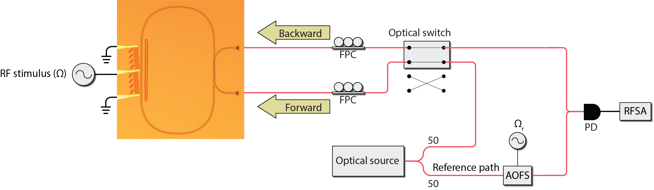
For measurement of optical signal transmission, and its Stokes and anti-Stokes sidebands, we utilize an optical heterodyne detection setup as shown in Fig. S5. The sources were kHz linewidth tunable external cavity diode lasers; specifically the New Focus model TLB-6728-P for 1520-1570 nm, and the New Focus model TLB-6712-P for 770–783 nm. The light is first split 50:50 into a device path and a reference path to enable heterodyne detection of the output light spectrum. Light in the reference arm was provided a predetermined offset (100 MHz for 1550 nm and 200 MHz for 780 nm) using an in-fibre acousto-optic frequency shifter. We used an optical switch (Thorlab model OSW22-1310E) to change the direction of the light for 1550 nm testing, while directionality was controlled manually for 780 nm testing. The minimum per-grating coupler losses are dB for 1550 nm and dB for 780 nm gratings, and are factored out in our measurements. Temporal interference of the light from the device path and the reference path was performed by a high-frequency photodetector (Thorlabs model RXM25AF for 1550 nm and RXM25DF for 780 nm). Further information on the experimental setup and heterodyne detection can be found in [1].
S7 Review of state of the art in on-chip optical isolators
A comparison of monolithically integrated, non-frequency shifting, linear response isolators is presented in Table S1. We exclude non-reciprocal modulators [1, 2, 13, 14, 19, 17] from this comparison since the insertion loss and isolation contrast are not well defined (i.e. the definitions are architecture-dependent and author-dependent).
Magneto-optic isolators consistently exhibit larger bandwidth than both electro-optic and acousto-optic isolators. Waveguide-based implementations consistently exhibit greater bandwidth than resonator-based isolators.
Since isolators can be cascaded, citing insertion loss (IL) or isolation contrast (IC) alone is not meaningful. Instead, the ratio of IC per dB of IL is the relevant figure of merit (FoM) for isolators [11]. We find that our best device not only provides contrast at par with the best magneto-optic isolators, but also outperforms them in insertion loss and the isolator FoM.
| Author | Year | Device Type | Technique | Peak isolation contrast (IC) | Insertion loss (IL) | Peak IC per 1 dB IL (dB/dB) | 10 dB IC Bandwidth | 20 dB IC Bandwidth | Wavelength |
| This work | - | Resonator | AO | 39.31 dB | 0.65 dB | 60.46 | 108.8 MHz | 33.1 MHz | 1550 nm |
| This work | - | Resonator | AO | 12.75 dB | 1.13 dB | 11.28 | 198.5 MHz | N/A | 1550 nm |
| This work | - | Resonator | AO | 12.86 dB | 4.76 dB | 2.7 | 202 MHz | N/A | 780 nm |
| Kim et. al. [12] | 2021 | Resonator | AO | 3 dB | 9 dB | 0.33 | N/A | N/A | 1550 nm |
| Dostart et. al. [7] | 2021 | Resonator | EO | 13.1 dB | 18.1 dB | 0.18 | 2 GHz | N/A | 1550 nm |
| Doerr et. al. [5] | 2014 | Waveguide | EO | 6 dB | 4 dB | 0.66 | N/A | N/A | 1550 nm |
| Tzuang et. al. [20] | 2014 | Waveguide | EO | 2.4 dB | N/A | N/A | N/A | N/A | 1550 nm |
| Lira et. al. [16] | 2012 | Waveguide | EO | 3 dB | 70 dB | 0.04 | N/A | N/A | 1550 nm |
| Doerr et. al. [6] | 2011 | Waveguide | EO | 2 dB | 11 dB | 0.18 | N/A | N/A | 1550 nm |
| Yan et. al. [21] | 2020 | Resonator | MO | 28 dB | 1 dB | 28 | 6.2 GHz † | 1.2 GHz † | 1550 nm |
| Yan et. al. [21] | 2020 | Waveguide | MO | 32 dB | 2.3 dB | 13.91 | 1.6 THz † | 490 GHz † | 1550 nm |
| Pintus et. al. [18] | 2019 | Waveguide | MO | 30 dB | 18 dB | 1.67 | 1.7 THz † | 582 GHz † | 1550 nm |
| Zhang et. al. [22] | 2019 | Waveguide | MO | 30 dB | 5 dB | 6 | 1.1 THz † | 249.7 GHz † | 1550 nm |
| Zhang et. al. [22] | 2019 | Resonator | MO | 20 dB | 11.5 dB | 1.739 | 1.2 GHz † | N/A† | 1550 nm |
| Du et. al. [8] | 2019 | Resonator | MO | 40 dB | 3 dB | 13.3 | 6.2 GHz † | 3.1 GHz† | 1520 nm |
| Bi et. al. [3] | 2019 | Resonator | MO | 19.5 dB | 8 dB | 2.6 | 1.6 GHz | N/A | 1520 nm |
| Huang et. al. [10] | 2017 | Resonator | MO | 14.4 dB | 10 dB | 1.44 | 12.4 GHz † | N/A | 1550 nm |
| Ghosh et. al. [9] | 2012 | Waveguide | MO | 25 dB | 14 dB | 1.78 | 99 GHz † | 31 GHz † | 1490 nm |
AO = Acousto-optic. EO = Electro-optic. MO = Magneto-optic. N/A = Information not available or not applicable.
† Estimated from the data shown in the publication.
| Parameters | Unit | 1550 nm isolator in Fig. 3a | 1550 nm isolator in Fig. 4 | 780 nm isolator in Fig. 3b | |
| of TE00 and TE10 modes (1 - 2) | GHz | 3 | 3.72 | 5.05 | |
| Total loss rate of TE00 mode (1) | GHz | 0.11 | 0.2 | 0.17 | |
| Total loss rate of TE10 mode (2) | GHz | 1.03 | 0.98 | 1.62 | |
| Quality factor of TE00 mode (Q1) | - | 1.76 106 | 0.97 106 | 2.25 106 | |
| Two-mode optical WGR | Quality factor of TE10 mode (Q2) | - | 1.88 105 | 1.97 105 | 2.36 105 |
| External coupling rate (ex1) | GHz | 0.01 | 0.04 | 0.01 | |
| External coupling rate (ex2) | GHz | 0.64 | 0.81 | 0.94 | |
| Wave number difference ( k1 - k2 ) | m-1 | 2.47 105 | 2.47 105 | 6.45 105 | |
| Center Wavelength | nm | 1556 | 1526 | 773 | |
| Transverse wave number (qtransverse) | m-1 | 2.84 106 | 2.84 106 | 5.19 106 | |
| Propagating wave number (qpropagating) | m-1 | 2.47 105 | 2.47 105 | 6.45 105 | |
| Total wave number (qtotal) | m-1 | 2.85 106 | 2.85 106 | 5.23 106 | |
| Surface Acoustic Wave | IDT Pitch () | m | 2.2 | 2.2 | 1.2 |
| IDT Aperture (W) | m | 400 | 400 | 300 | |
| IDT Angle () | degree | 4.98 | 4.98 | 7.08 | |
| Center frequency () | GHz | 3 | 3.04 | 5.05 | |
| Acousto-optic Interaction | Phonon-enhanced optomechanical coupling | GHz | 0.97 (29 dBm) | 0.76 (29 dBm) | 0.98 (25 dBm) |
References
- [1] Cited by: §S1, §S1, §S3, §S3, §S5, §S6, §S7.
- [2] (2019/12/01) Direction reconfigurable nonreciprocal acousto-optic modulator on chip. APL Photonics 4 (12), pp. 126103. Note: doi: 10.1063/1.5123497 External Links: Document Cited by: §S7.
- [3] (2011) On-chip optical isolation in monolithically integrated non-reciprocal optical resonators. Nat. Photonics 5 (12), pp. 758. Cited by: Table S1.
- [4] (2000-07) Observation of critical coupling in a fiber taper to a silica-microsphere whispering-gallery mode system. Phys. Rev. Lett. 85, pp. 74–77. External Links: Document Cited by: §S2.
- [5] (2014-02) Silicon photonics broadband modulation-based isolator. Opt. Express 22 (4), pp. 4493–4498. External Links: Document Cited by: Table S1.
- [6] (2011-11) Optical isolator using two tandem phase modulators. Opt. Lett. 36 (21), pp. 4293–4295. Cited by: Table S1.
- [7] (2021) Optical isolation using microring modulators. Optics Letters 46 (3), pp. 460–463. External Links: Document Cited by: Table S1.
- [8] (2018/12/19) Monolithic on-chip magneto-optical isolator with 3 dB insertion loss and 40 db isolation ratio. ACS Photonics 5 (12), pp. 5010–5016. Note: doi: 10.1021/acsphotonics.8b01257 External Links: Document Cited by: Table S1.
- [9] (2012-01) Ce:YIG/Silicon-on-insulator waveguide optical isolator realized by adhesive bonding. Opt. Express 20 (2), pp. 1839–1848. External Links: Document Cited by: Table S1.
- [10] (2017) Dynamically reconfigurable integrated optical circulators. Optica 4 (1), pp. 23–30. Cited by: Table S1.
- [11] (2017) Complete linear optical isolation at the microscale with ultralow loss. Sci. Rep. 7 (1), pp. 1647. Cited by: §S7.
- [12] (2021/01/01) On-chip optical non-reciprocity through a synthetic hall effect for photons. APL Photonics 6 (1), pp. 011301. Note: doi: 10.1063/5.0034291 External Links: Document Cited by: Table S1.
- [13] (2021) Electrically driven acousto-optics and broadband non-reciprocity in silicon photonics. Nature Photonics 15 (1), pp. 43–52. External Links: Document, ISBN 1749-4893 Cited by: §S7.
- [14] (2018-10) Non-reciprocal interband Brillouin modulation. Nat. Photonics 12 (10), pp. 613–619. External Links: ISSN 1749-4893 Cited by: §S7.
- [15] (2001-01) Investigation of acoustic waves in thin plates of lithium niobate and lithium tantalate. IEEE Transactions on Ultrasonics, Ferroelectrics, and Frequency Control 48 (1), pp. 322–328. External Links: Document, ISSN 1525-8955 Cited by: §S5.
- [16] (2012) Electrically driven nonreciprocity induced by interband photonic transition on a silicon chip. Phys. Rev. Lett. 109, pp. 033901. Cited by: Table S1.
- [17] (2019-06) Electromechanical Brillouin scattering in integrated optomechanical waveguides. Optica 6 (6), pp. 778–785. Cited by: §S7.
- [18] (2019-03) Broadband te optical isolators and circulators in silicon photonics through ce:yig bonding. Journal of Lightwave Technology 37 (5), pp. 1463–1473. External Links: Document, ISSN 1558-2213 Cited by: Table S1.
- [19] (2020) Acousto-optic modulation of a wavelength-scale waveguide. arXiv:2010.12517. Cited by: §S7.
- [20] (2014-08) Non-reciprocal phase shift induced by an effective magnetic flux for light. Nat. Photonics 8, pp. 701. Cited by: Table S1.
- [21] (2020-11) Waveguide-integrated high-performance magneto-optical isolators and circulators on silicon nitride platforms. Optica 7 (11), pp. 1555–1562. External Links: Document Cited by: Table S1, Table S1.
- [22] (2019-04) Monolithic integration of broadband optical isolators for polarization-diverse silicon photonics. Optica 6 (4), pp. 473–478. Cited by: Table S1, Table S1.