S-shaped current-voltage characteristics of n+-i-n-n+ graphene field-effect transistors due to the Coulomb drag of quasi-equilibrium electrons by ballistic electrons
Abstract
Keywords: graphene, field-effect transistor, ballistic electrons, Coulomb electron drag, S-shape current-voltage characteristics.
We demonstrate that the injection of the ballistic electrons into the two-dimensional electron plasma in lateral n+-i-n-n+ graphene field-effect transistors (G-FET) might lead to a substantial Coulomb drag of the quasi-equilibrium electrons due the violation of the Galilean and Lorentz invariance in the systems with a linear electron dispersion. This effect can result in the S-shaped current-voltage characteristics (IVs).
The resulting negative differential conductivity enables the hysteresis effects and current filamentation
that can be used for the implementation of voltage switching devices.
Due to a strong nonlinearity of the IVs, the G-FETs can be used for an effective frequency multiplication and detection of terahertz radiation.
I Introduction
The lateral transport of electrons and holes in the graphene layer (GL) heterostructures could enable the detection, amplification, and generation of terahertz radiation [1, 2] and other numerous applications (see, for example, [3]). In this paper, we analyze the electron transport in the lateral n+-i-n-n+ graphene field-effect transistors (G-FETs) with the n+ source and drain contacts and the gated n-region. Figure 1 shows the G-FET structure and the band diagrams at different source-drain voltage: and , where meV is the optical phonon energy in graphene and is the electron charge. The n-region is formed by the positive gate bias . Similar lateral heterostructure GL devices including those based on more complex lateral periodical cascade devices were reported previously [1, 2, 3, 4, 5, 6, 7]. One of the remarkable advantages of the GLs is the possibility of very high directed velocities of the electron (hole) ensembles close to the characteristic velocity cm/s [6, 7] providing the collision-less, i.e., ballistic electron (BE) motion [8, 9] in relatively long channels. As demonstrated experimentally, in the graphene encapsulated in hexagonal boron nitride the ballistic transport is realized in the samples with the length of a few m at room temperature [10] and of 28 m at decreased temperatures [11].
As was predicted decades ago [9], the BE motion interrupted by the emission of the optical phonons can enable the self-excitation of the current oscillations leading to the radiation emission [12, 13, 14, 15, 16].
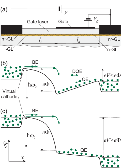
Considering the lateral forward-biased n+-i-n-n+ G-FET with the sufficiently perfect GL, we assume that the transport of the injected electrons from the emitter n+ region into the i-region (, where is the i-region length) is ballistic. This implies that the BE transit time in the i-region is much shorter that the characteristic times of their scattering on the impurities and the acoustic phonons, and . The impurity and acoustic phonon scattering of the BEs injected into the n-region (, where stands for the n-region length) is also insignificant. Thus, . We demonstrate that the Coulomb collisions of the BEs, injected into the n-region, with the thermalized quasi-equilibrium electrons (QEs) can lead to the ”conversion” of a fraction of these electrons into the dragged equilibrium electrons (DQEs) moving toward the n+ collector drain region (analogous to the mutual electron-hole drag). Such a Coulomb drag in GLs, i.e., in the electron systems with the linear energy spectrum can be fairly effective. The GL electron system is neither a Galilean nor a truly Lorentz-invariant system [17, 18, 19]. The Coulomb drag in question is fundamentally similar to the drag between spatially separated standard [20, 21] and graphene-based [22, 23, 24, 25, 26, 27, 28, 29] two-dimensional electron-hole systems. This effect was extensively studied in graphene both theoretically and experimentally (see, for example, [22, 23, 27]). An essential distinction of the ballistic-equilibrium drag is the current non-conservation (and possible multiplication) due to electron-electron collisions. The Coulomb electron drag in the G-FETs under consideration with the current multiplication might pronouncedly affect the device characteristics resulting in the S-type current-voltage characteristics (IVs). The latter can lead to the hysteresis phenomena and the instability of the uniform current flow (the current filamentation).
Similar phenomenon can take place in the reverse-biased p+-p-i-n-n+ devices [6, 7] due to the interband tunneling generation [23, 24] of the electron-hole pairs in the i-region.
The physics behind is the Coulomb drag by the BEs. BEs collisions with QEs results in the latter contributing to the current. As a result, the current voltage characteristic is nonlinear even at low applied voltages, since the voltage increase results in a higher level of the BE injection. At a certain threshold voltage, this nonlinearity might lead to the infinite differential conductance. At the threshold voltage, the switching occurs into another stable branch of the current-voltage characteristic with the dominant contribution of the BEs. As a consequence, there are two stable branches of the IV: (a) the low current branch with a relatively few injected BEs and (b) the high current branch with the dominant BE transport. The switching occurs at the threshold voltage and the value of current after switching depends on the load line (i.e. on the load resistance). During the switching, the current traverses the unstable branch with the negative differential conductance. Depending on the load resistance and on the applied voltage, the final state might correspond to the current filamentation when the device cross section is divided into regions corresponding to the low current and high current branches, respectively
The paper is organized as follows. In Sec. II, we find the potential distribution in the G-FET injection region (i-region) and derive the injected current density as a function of the potential drop across this region. Section III deals with the analysis of the Coulomb drag of the QEs by the BEs. In this section, the net current density in the n-region is expressed as a sum of the BEs, DQEs, and QEs. Using the results of Sec. III, we derive the IVs in Sec. IV and demonstrate that they can be both monotonic and S-shaped. In Sec. V, we consider the possibility of the current switching in the G-FETs enabled by the S-shape of their IVs. Section VI deals with the instability of uniform current spatial distributions at the fixed terminal current, which, as indicated, can lead to the formation of the stationary and pulsing current filaments. Section VII is devoted to the comments associated with the device model. In Conclusions (Sec. VIII) we summarize the main results of the paper. Some, mainly intermediate mathematical results, are given in Appendix A and Appendix B.
II Potential distribution and injected current
The injection current density is determined by the voltage drop across the GL i-region and by the space charge in this region (the space-charge-limited electron injection [30]). The potential is determined by the potential spatial distribution across the entire G-FET structure corresponding to the boundary conditions and , where and are the lengths of the i- and n-regions. For the lateral G-FET structure with the blade-like regions near the i-region edges and for the injected BE density (where cm/s is the characteristic electron velocity in GLs and is the electron charge) the potential distribution across the i-region satisfying the conditions and , and versus relation can be found as follows (compare with, for example, [30, 31, 32, 33]):
| (1) |
| (2) |
Here is the dielectric constant of the material surrounding the GL. To consider the regime of electron injection limited by the electron space charge near the source n-i-junction, we set the electric field at a point (the ”virtual cathode” [30], see Fig. 1) to be equal to zero. Accounting for Eq. (2), this condition yields
| (3) |
Equations (1) - (3) are valid when , where is the temperature in the energy units. Equation (3) is in line with the well known result obtained for the devices with blade-like injection contacts (but for the carrier transport with the saturation velocity ). However, Eq. (3) yields different voltage dependence from those found for different bulk contacts [4].
Hence, according to Eqs. (1) and (2), we obtain
| (4) |
| (5) |
Thus, and ). Here, is the thickness of the gate layer.
III Coulomb electron drag
The BEs injected into the n-region have the energy and the momentum . The collisions between the injected BEs and QEs in the n-region result in the transfer of a part of the ballistic electron momentum to the QEs. Due to the linearity of the electron spectrum in GLs, the injected and the BEs scattered by the QEs with small energies preserve the direction of their movement (in the direction from the emitter to the collector), while their directed momentum changes from to . Despite the lost portion of the momentum, the BE continues its motion toward the collector with the same velocity . Due to the collision with the BE, the QE receives the momentum . According to the energy and momentum conservation laws for the linear electron energy dispersion relation, the QEs also move with the velocity in the -direction, so that, in contrast to both bulk and conventional two-dimensional semiconductor systems, the momentum conservation at the electron-electron collisions does not lead to the velocity conservation [17]. In other words, a portion of the QEs becomes excited with the average directed momentum and velocity upon collisions with the injected BEs.
Thus, the electron collisions between the injected BEs and the QEs convert QEs into BEs doubling of the net current carried by the original and ”secondary” BEs. Hence, the BE current density (associated with the original BEs, which came from the i-region, and the QEs dragged by the BEs, to which we refer to as the DQEs) in the n-region () can exceed the BE current density in the i-region. This we interpret as the amplified QE drag by the injected BEs.
The spatial variation of the BE current density across the n-region due to the BEs scattering on the QEs and optical phonons is determined by
| (6) |
with where
| (7) |
| (8) |
Here , , and [33, 34, 35, 36] are the characteristic times of the electron-electron (BEs on QEs) scattering, and the BE scattering on acoustic and optical phonons, and are the GL density and the optical deformation potential, respectively, and is the unity step function reflecting the threshold character of the optical phonon emission. To account for the temperature and electron spectrum smearing of the optical phonon emission threshold, we set with being the QE temperature. The linear factor in the expression for is associated with the linearity of the GL density of states near the Dirac point. The Fermi electron energy in the gated n-region, , appears in the latter function argument to account for the optical phonon emission with the electron transitions to the states above the Fermi level. For simplicity we neglect the BE scattering on impurities not only in the i-region, but in the n-region as well because in the G-FETs under consideration with the gated n-region the electrons are primarily induced by the gate voltage (not by ionized impurities). The quantity markedly exceeds . At the electron densities cm-2 and room temperature one can set for the energy of the BEs injected into the n-region ps-1, ps-1, and ps-1 [17, 33, 34, 35, 36, 37, 38]. If m, we find , , and . At lower temperatures, becomes even smaller. For brevity we do not distinguish the different intra-valley and inter-valley optical phonon modes using for their energies the common value meV and accounting for the contribution of both modes by choosing the proper scattering time .
Since , where is given by Eq. (3), as follows from Eq. (6), one obtains for the density of the BE current injected into the n+-contact at
| (9) |
The BEs colliding with the QEs in the n-region transfer to the latter the average (per one QE) momentum equal to
| (10) |
where is the QE density. We have disregarded a weak spatial nonuniformity of the electron density in this region , where the density of the ionized donors and is the electron density induced by the gate voltage (the effect of the quantum capacitance is disregarded for simplicity as well).
The QE drag resulting in the QEs direct momentum induces the QE current, so that the density of the net current (associated with the injection of the BEs), into the collector n+-region can be presented as
| (11) |
Here is the QE average velocity caused by the QE drag. It is related to [see the Appendix, Eqs. (A3) and (A5)] as
| (12) |
Here is a coefficient determined by the QE statistics, where is the QE Fermi energy (see, Appendix A).
| Voltage, | |||
|---|---|---|---|
| Current density, |
IV Characteristics
IV.1 General equations
Taking into account that the leakage of the QEs from the n-region associated with the drag is compensated by the conductivity current (so that the net current density in the n-region ), we arrive at the following equation relating the current density , potential , and applied voltage :
| (13) |
Considering Eq. (3), Eq. (13) can be presented as a relation between the potential and the bias voltage
| (14) |
Here with [see Eq. (3)]. The parameter is actually the ratio of the i-region resistance and the n-region resistance (per unit length in the direction perpendicular to the current flow): . At the QE mobility cm2/sV, cm-2, and , one obtains .
Equation (14) yields the following source-drain voltage-current characteristics
| (15) |
with , , and is the Coulomb drag parameter (see Appendix A). This parameter determines the ratio of the current created by the DQEs and the current of the injected BEs, which is equal to . When the potential drop across the i-region , the optical phonon emission is blocked, i.e., , (see below). The parameters and are crucial for the distribution of the potential drops across the i- and n-regions. Due to the dependence of the parameter on the Fermi energy , this parameter is controlled by the gate voltage : . Setting meV, meV ( cm-2), and , we obtain . At and m, we arrive at the following estimate: A/m.
IV.2 Low current densities
In the voltage and current density ranges where , , and , so that the optical phonon emission is not involved in the IV formation, we obtain from Eqs. (14) and (15)
| (16) |
Here and in the following we omit the term .
As follows from Eq. (16), at a certain voltage , where
| (17) |
one obtains . This point corresponds to
| (18) |
Equation (16) describes the IV lower branch in Fig. 2. It also describes the IV middle branch if the latter exist, that happen if and as seen in Fig. 2.
Naturally, in the absence of the Coulomb drag (), such a voltage point does not exist ( tends to infinity). Equation (16) also corresponds to , i.e., the negative differential conductivity, when .
IV.3 High current densities
When , , and . In this case, the optical phonon emission starts to play a substantial role. Accounting for such an emission, from Eq. (14) we obtain the following generalization of Eq. (16):
| (19) |
where we have introduced the normalized electron Fermi energy . In particular, Eq. (19) describes the IV upper branch with , i.e., characterized by a monotonic potential distribution shown in Fig. 1(c).
The IV governed by Eq. (19) exhibits the point near the threshold of the optical phonon emission, where , , corresponding to , for relatively small , are close to
| (20) |
| (21) |
If , one can expect that markedly exceeds , so that , and the drag effect is suppressed by the relaxation of the BE momentum due to the optical phonon emission. In such a limit, the high-voltage section of the IV becomes monotonically rising.
IV.4 IV peculiar points
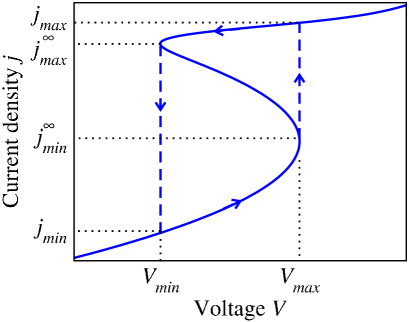
As follows from the above analysis, the IVs exhibit the following peculiar points (for ), see also Table I:
(a) and ;
(b) and
;
(c) and ,
with ;
(d) and ;
(e) and
with .
The net current is a monotonic function of the bias voltage if , i.e., if . In the opposite case , i.e., when , the IVs are of the S-shaped form with a region of the negative differential conductivity . The latter corresponds to the voltage range .
Figure 2 shows the schematic view of the G-FET S-shaped IV (analogous to those in the following Figs. 3 - 5) at the parameters and
corresponding to with the indicated peculiar points corresponding to Table I.
In
situations when the source-drain voltage is given, the G-FET source-drain IVs can be of the S-shape.
IV.5 Results of numerical calculations
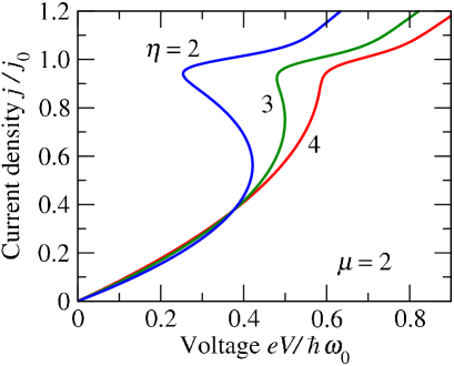
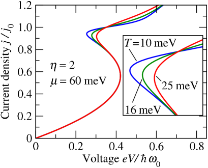
Figure 3 shows the IVs calculated for , , , , ( meV), meV ( K) and different values of other parameters ( and ) demonstrating their transformation from the monotonic to S-shaped characteristics. As seen from Fig. 3, an increase in (for example, due to a decrease in the n-region resistance) leads to a weakening of the S-shape with a shift of toward larger values.
As follows from Eq. (19), the IV shape varies with changing parameter , i.e., with changing the Fermi energy , which, in turn, depends on the gate voltage . The variation of results in the variation of not only the parameter , characterizing the drag effect, but the variation of the parameter , determining the density of electron states near the threshold of the optical emission, as well. Since in the G-FETs under consideration, the dominant QE scattering mechanism is associated with the acoustic phonons (short-range scattering mechanism, which is the same as for neutral impurities and point defects), the gated n-region conductivity and, therefore, can be set independent of [39, 40]. The change in and, consequently in the QE density affects . However, this can be disregarded until , i.e., until the QE density is not too small.
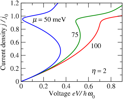
Figure 4 shows the G-FET IVs calculated using Eq. (19) for and different values of the Fermi energy . The same other parameters and the temperature are assumed as for Fig. 3. One can see that the IV shape is fairly sensitive to the QE Fermi energy in the gated n-region , i.e., depends on the QE density and, hence, on the gate voltage . An increase in can result in the transformation from the S-shaped IVs to the monotonic IVs. This is attributed to a weakening of the drag effect with increasing (see below).
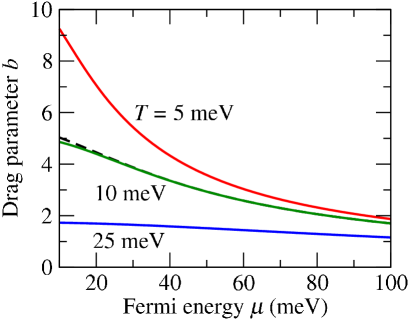
An increase in the temperature beyond meV leads to the IVs with a less pronounced S-shape, although such characteristics could be obtained even at room temperature if the parameters are chosen properly, in particular, by chosing sufficiently, small and ( meV). Indeed, choosing meV and (other parameters are the same as in Figs. 3 and 4), we arrive at the S-shaped IVs shown in Fig. 5, corresponding to the temperature range from meV to meV. As seen, for the latter set of the parameters the S-shape can be preserved even at room temperature. The temperature smearing of the threshold of the optical phonon emission leads to a small deviation (for moderate values ) of the peculiar point positions from the values given in Table I. The effects of the Fermi energy and the temperature variations on the IVs are attributed to the Coulomb drag parameter versus and dependences. Figure 6 shows examples of these dependences calculated using Eq. (A7) in Appendix A. Assuming that , in the calculations of we set . One can see that a decrease in and provides a rise of (and, therefore, the IVs with a more pronounced S-shape).
V Current switching by the voltage pulses
The S-shaped IVs with hysteresis can enable the bistable operation controlled by the source-drain voltage. At the fixed source-drain voltage in the voltage range , there are two branches of the stable states: the ”low” stable with the current densities and the ”high” stable with . The stability of these states is due the positive differential conductivities and at the pertinent branches. In contrast, the states in the intermediate branch are unstable (see below).
The transition from the low state to the high state requires the voltage pulse . The reverse transition can be realized by applying the voltage pulse . The pulse duration should be sufficiently longer than the characteristic time of the temporal relaxation of the electron system . This time, as is estimated in the next section, can be an order of a few ps.
Hence, the G-FETs with the S-shaped IVs can be used for the frequency multiplication of the incoming signals. A strong IV nonlinearity at certain applied voltages can be also used for the signal rectification and, therefore, for the signal detection.
VI Aperiodic instability of uniform current flow
In the devices with the S-shaped IVs the current tends to filamentation under the condition when the net terminal current is fixed. This is due to the instability of the uniform state of the electron plasma toward the spatial perturbations in the in-plane -direction, perpendicular to the current flow (in the -direction).
Let us consider the dynamic behavior of the electron system. Introducing the normalized average current density , where is the net current through the G-FET (which is maintained to be fixed) chosen to be such that is in the range of the negative differential conductivity), is the width in the -direction, and introducing
| (22) |
| (23) |
we present an equation governing the spatio-temporal variations in the gated n-region given in Appendix B [Eq. (B1)] in the following form:
| (24) |
The quantity is a product of the gated n-region capacitance and the G-FET source-drain resistance .
Now we focus on the stability of the uniform current flow with . Assuming that the potential , where and are the wave number and the frequency of the perturbation, respectively, we obtain from Eq. (23) the following dispersion equation for the transit potential perturbations:
| (25) |
When
| (26) |
the right-hand side of Eq. (25) is negative. This corresponds to falling to the current range , in which, as mentioned above, the differential conductivity is negative. In this current range, Eq. (25) for the electron plasma perturbations increment (the grows rate) yields
| (27) |
which is positive for sufficiently small wave numbers , i.e., for sufficiently long perturbations. However, the perturbation length is limited by the device size, , in the -direction.
Since, according to Eq. (25), Re , inequality (26) corresponds to a temporal aperiodic rise of the plasma perturbations (aperiodic plasma instability). Hence, the temporal variation of the electron system out of equilibrium, including the transformation of the current spatial distribution and the duration of the switching process is characterized by the time given by Eq. (22). Setting, for example, , m, m, and m, for the characteristic time, , determining the time scale of the dynamic processes in the G-FETs, we obtain ps.
Setting (that corresponds to the dc potential at equal to mV, i.e., mV), meV, and meV (), from Eq. (27) we find that the plasma instability in question can occur if .
The current instability associated with the S-type IVs is akin to those predicted by B. K. Ridley (see, for example, [41, 42, 43, 44, 45]), although it is caused by a different mechanism, namely, by the electron drag.
As can be concluded from Eq. (27), the spatial scale of the current filaments is determined by the characteristic length given by Eq. (23). Hence, the filamentation is possible when the width of the G-FET in the y-direction . Setting m and , we find m. Depending on the boundary conditions at the G-FET edges (in the -direction, and ), the arising filaments cam be either stationary or pulsating. The formation of the nonlinear filament structure might change the source-drain voltage drop at the fixed net current. In the case of the pulsating filaments, the source-drain voltage can comprise an ac component.
VII Comments
VII.1 Origin of the S-shaped IVs
As shown above, at sufficiently strong drag effect (large ), the IVs can be of the S-shape. This is associated with the following two reasons: First, if the potential drop across the i-region is smaller than the voltage corresponding to the optical phonon emission, there the IV ambiguity with two possible values of the current: a relatively low with a small contribution of the DQEs and rather large with a marked contribution of the DQEs [this ambiguity is described by Eq. (16)]. In the first case, the potential difference removes the injected BEs that have accumulated in the n-region. Such a low IV branch corresponds to an elevated source-drain voltage [see Fig. 1(c)]. In contrast, in the second case, the DQE current through the n-region is compensated by the reverse current injected from the drain. The latter requires , i.e., a lowered voltage as seen from Fig. 1(b). Second, when is sufficient for the emission of optical phonons by the injected BEs (near the point separating the i- and n-region), the drag suppressed, and the transport become normal, i.e., with the monotonic potential distribution. The latter situation corresponds to the upper branch of the S-shaped IV. In the less probable case of too large parameter , the upper branch can appear because of reflection of the DQEs by a strong braking electric field .
VII.2 Electron injection and transit-time delay
In the case of the lateral n+-contact, the BE injection is limited by the two-dimensional space-charge in the i-region. The G-FETs with the BE tunneling injection through the Schottky contact can exhibit a similar behavior. However, in the latter case, the versus relation can be different [a nonlinear in contrast to Eq. (3)]. This can lead to a modification of the IVs in comparison with derived above.
At AC voltage, the density of the BE current injected into the n-region exhibits a delay due to the finite transit time of the BEs across the i-region. Such a BE transit delay can, in principle, affect the transient processes in the G-FETs under consideration, in particular, the dynamic of the instability considered above.
According to the Shockley-Ramo theorem [46, 47], one needs to replace the quantity (which constitutes the quasi-stationary current density) in the right-hand side of Eq. (9) by the current density of the BEs propagating across the i-region. Therefore, the ac component of the induced current density can be presented as [6, 7]
| (28) |
where is the Bessel function and the factor under the integral appears due to the electric field created by the BEs in the case of the ”blade-shaped” highly conductive n+- and gated n-regions [48].
According to Eq. (28), the relative role of the transit-time effect is weak in comparison with the effect of the gated n-region RC-recharging is characterized by the ratio . Taking into account Eq. (22), we find .
For , m, m, one obtains . Since the latter inequality is normally satisfied for the G-FETs with realistic parameters, we disregarded the BE transit delay, although this effect can lead to a moderate decrease of the instability increment.
VII.3 Plasmonic resonance effects
The two-dimensional electron system in the gated n-region of the GL channel can exhibit the plasmonic resonances corresponding to the plasma oscillation frequencies and its harmonics [49]. The excitation of the plasma oscillations is possible when the source-drain voltage comprises the ac component with the frequency . This component can be associated with the incident radiation received by an antenna. This effect combined with the pronounced IV nonlinearity should lead to a resonantly large rectified current, which can be used for the detection of the incoming radiation. According to the estimate of the plasma frequency , it can be in the terahertz frequency (THz) range. Due to the positive feedback between the currents injected to the i-region from the source and the reverse current injected to the n-region from the drain, one might expect the plasma instability of the net steady-state source-drain current resulting in the self-excitation of the THz plasma oscillations [50]. However, the analysis of such effects is beyond the scope of the present paper.
VII.4 Technological aspects
The crystallographic quality of graphene synthesized by a popular engineering method of the thermal decomposition from the SiC substrate is now approaching the high end of those for exfoliated graphene [51], in particular, exhibiting the BE transport [10, 11]. The G-FET (similar to that under consideration in this paper) process technology is getting matured for both semiconductor integrated device processes based on e-beam lithography and gate stack formation with the plasma chemical vapor deposition (CVD) [52] or the atomic layer deposition (ALD) and exfoliation and dry-transfer in hBN/graphene/hBN van der Waals hetero-stacking for the gate stack [1]. The processed GL channels in those G-FET devices with sub-micrometer dimensions exhibit field-effect mobilities beyond 100,000 cm2/Vs [51, 52].
VIII Conclusions
We proposed and evaluated the characteristics of a lateral n+-i-n-n+ G-FET with the ballistic transport of the electrons injected from the source n+-region into the i-region. We demonstrated that the ballistic electrons entering the n-region can effectively drag the quasi-equilibrium electrons toward the drain if the electron-electron scattering in the gated n-region prevails over the impurity and acoustic phonon scattering. The Coulomb ballistic-equilibrium electron drag in question with the electron current multiplication is associated with the linearity of the electron energy dispersion law in graphene. The drag effect can result in non monotonous potential distributions in the G-FET channel and the strongly nonlinear S-type source-drain IVs. The S-type IVs might lead to the filamentation of the current in the G-FET channel (with the stationary or pulsating filaments) and to the hysteresis phenomena, enabling the switching between different current states. Apart from this application, the plasmonic phenomena in the G-FETs under consideration can be used for the THz radiation detection, generation, and signal frequency-multiplication. The latter applications require a separate consideration.
Acknowledgments
The work at RIEC and UoA was supported by Japan Society for Promotion of Science, KAKENHI Grant Nos. 21H04546, 20K20349, Japan; RIEC Nation-Wide Collaborative research Project No. H31/A01, Japan; The work at RPI was supported by Office of Naval Research (N000141712976, Project Monitor Dr. Paul Maki). The authors are grateful to D. Svintsov for very useful discussions. One of the authors (V.R.) is also thankful to Yu. G. Gurevich for helpful information.
Appendix A. QE Coulomb drag parameter
The average momentum transferring from BEs to QEs (per one QE) can be presented as:
| (A1) |
The QE distribution function
| (A2) |
whee is the average drift velocity obtained by QEs due to the collisions with the BE flux, is temperature and is the electron Fermi energy: . The latter yields the relation between and :
| (A3) |
where
| (A4) |
Here is the Fermi-Dirac integral. At , .
Hence,
| (A5) |
Using Eq. (A4), the quantity , which we call as the Coulomb drag parameter, is presented as
| (A6) |
When , . Since Fermi energy depends on the QE density , and, therefore, are controlled by the gate voltage .
If the value of approaches to the Dirac point, the drag of the quasi-equilibrium holes (QHs) can become crucial. This is because the QHs are dragged by the BEs to the same direction partially neutralizing the current of the dragged QEs.
Considering that the QH Fermi energy is equal to , one can obtain the expression for the drag parameter replacing Eq. (A6):
| (A7) |
Equation (A7) does not account for the mutual electron-hole drag [18]. The latter should lead to a somewhat smaller value of in comparison with Eq. (A6). Thus the QHs weaken the drag current multiplication. Although for the G-FETs with the parameters used in the main text, this is negligible.
For different devices with the two-dimensional carriers but with the quadratic dispersion (having the 2D channels in the heterostructures made of the standard materials and the graphene bilayer heterostructures), , where is the carrier effective mass) and , so that there is no electron current multiplication.
Appendix B. Spatio-temporal variations of electron system in the gated region
The electron charge in the diode active region () , where is the gated n-region capacitance, obeys the following equation:
| (B1) |
The factor 1/2 in the second term in the left-hand side of Eq. (B1), appears because the potential in the n-region varies between and (approximately linearly). Equation (B1) can be presented as
| (B2) |
In the case of the steady-state uniform current flow with when , Eq. (B1) is reduced to Eq. (24). If the average current density through the G-FET and its normalized value are given, Eq. (B2) can also be presented in the following form:
| (B3) |
Here and .
References
- [1] S. Boubanga-Tombet, W. Knap, D. Yadav, A. Satou, D. B. But, V. V. Popov, I. V. Gorbenko, V. Kachorovskii, and T. Otsuji, “Room temperature amplification of terahertz radiation by grating-gate graphene structures,”Phys. Rev. X 10, 031004-1-19 (2020).
- [2] J. A. Delgado-Notario, V. Clericò, E. Diez, J. E. Velazquez-Perez, T. Taniguchi, K. Watanabe, T. Otsuji, and Y. M. Meziani, “Asymmetric dual grating gates graphene FET for detection of terahertz radiations,”APL Photon. 5, 066102-1-8 (2020).
- [3] V. Ryzhii, T. Otsuji, and M. S. Shur, “Graphene based plasma-wave devices for terahertz applications,”Appl. Phys. Lett.116, 140501-1-6 (2020).
- [4] M. Ryzhii and V. Ryzhii, “Injection and population inversion in electrically induced p–n junction in graphene with split gates, ”Jpn. J. Appl. Phys. 46, L151 (2007).
- [5] M. Ryzhii, V. Ryzhii, T. Otsuji, V. Mitin, and M. S. Shur, “Electrically induced n-i-p junctions in multiple graphene layer structures,”Phys. Rev. B 82, 075419 (2010).
- [6] V. Ryzhii, M. Ryzhii, V. Mitin, and M. S. Shur, “Graphene tunnelinhg transit-time terahertz oscillator based on electrically induced p-i-n junctions,”Appl. Phys. Express 2, 034503 (2009).
- [7] V. L. Semenenko, V. G. Leiman, A. V. Arsening, V. Mitin, M. Ryzhii, T. Otsuji, and V. Ryzhii, “Effect of self-consistent electric field on characteristics of graphene p-i-n tunneling transit-time diodes,”J. Appl. Phys. 113, 024503 (2013).
- [8] M. S. Shur and L. F. Eastman, “Ballistic transport in semiconductor at low temperatures for low-power high-speed logic,”IEEE Trans. Electron Devices 26, 1677-1683 (1979).
- [9] V. I. Ryzhii, N. A. Bannov, and V. A. Fedirko, “Ballistic and quasi ballistic transport in semiconductor structures (review)”, Sov. Phys. Semicond. 18, 481 (1984).
- [10] A. S. Mayorov, R. V. Gorbachev, S. V. Morozov, L. Britnell, R. Jalil, L. A. Ponomarenko, P. Blake, K. S. Novoselov, K. Watanabe, T. Taniguchi, and A. K. Geim, “Micrometer-scale ballistic transport in encapsulated graphene at room temperature,”Nano Lett. 11, 2396-2399 (2011).
- [11] L. Banszerus, M. Schmitz, S. Engels, M. Goldsche, K. Watanabe, T. Taniguchi, B. Beschoten, and C. Stampfer, “Ballistic transport exceeding 28 m in CVD grown graphene,”Nano Lett. 16, 1387-1391 (2016).
- [12] A. A. Andronov and V. A. Kozlov, “Low-temperature negative differential microwave conductivity in semiconductors following elastic scattering of electrons,”JETP Lett. 17, 87 (1973).
- [13] V. L. Kustov, V. I. Ryzhii, and Yu. S. Sigov, “Nonlinear plasma instabilities in semiconductors subjected to strong electric fields in the case of inelastic scattering of electrons by optical phonons,”Sov. Phys. JEPT 99 (1980).
- [14] L. E. Vorob’ev, S. N. Danilov, V. N. Tulupenko, and D. A. Firsov, “Generation of millimeter radiation due to electric-field-induced electron-transit-time resonance in indium phosphide,”JEPT Lett. 73, 219 (2001).
- [15] S. Sekwao and J. P. Leburton, “Terahertz harmonic generation in graphene,”Appl. Phys. Lett. 106, 063109 (2015).
- [16] A. A. Andronov and V. I. Pozdniakova, “Terahertz dispersion and amplification under electron streaming in graphene at 300 K, ”Semiconductors 54, 1078-1085 (2020).
- [17] X. Li, E. A. Barry, J. M. Zavada, M. Buongiorno Nardelli, and K. W. Kim, “Influence of electron-electron scattering on transport characteristics in monolayer graphene,”Appl. Phys. Lett. 97, 082101 (2010).
- [18] D. Svintsov, V. Vyurkov, S. Yurchenko, T. Otsuji, and V. Ryzhii, “Hydrodynamic model for electron-hole plasma in graphene,”J. Appl. Phys. 111, 083715 (2012).
- [19] D. Svintsov, V. Ryzhii, A. Satou, T. Otsuji, and V. Vyurkov, “Carrier-carrier scattering and negative dynamic conductivity in pumped graphene,”Opt. Express 22, 19873 (2014).
- [20] T. J. Gramila, J. P. Eisenstein, A. H. MacDonald, L. N. Pfeiffer, and K. W. West, “Mutual friction between parallel two-dimensional electron systems,”Phys. Rev. Lett. 66, 1216 (1991).
- [21] U. Sivan, P. M. Solomon, and H. Shtrikman, “Coupled electron-hole transport,”Phys. Rev. Lett. 68, 1196 (1992).
- [22] M. Schütt, P. M. Ostrovsky, M. Titov, I. V. Gornyi, B. N. Narozhny, and A. D. Mirlin, “Coulomb drag in graphene near the Dirac point,”Phys. Rev. Lett. 110, 026601 (2013).
- [23] R. V. Gorbachev, A. K. Geim, M. I. Katsnelson, K. S. Novoselov, T. Tudorovskiy, I. V. Grigorieva, A. H. MacDonald, S. V. Morozov, K. Watanabe, T. Taniguchi, and L. A. Ponomarenko, “Strong Coulomb drag and broken symmetry in double-layer graphene,”Nat. Phys. 8, 896 (2012).
- [24] J. C. Song, D. A. Abanin, and L. S. Levitov, “Coulomb drag mechanisms in graphene,”Nano Lett. 13, 3631 (2013).
- [25] D. Svintsov, V. Vyurkov, V. Ryzhii, and T. Otsuji, “Hydrodynamic electron transport and nonlinear waves in graphene, ”Phys. Rev. B 88, 245444 (2013).
- [26] S. H. Abendinpour, G. Vignale, A. Principi, M. Polini, W.-K. Tse, and A. H. MacDonald, “Drude weight, plasmon dispersion, and ac conductivity in doped graphene sheets,”Phys. Rev. B 84, 045429 (2011).
- [27] J. Li, T. Taniguchi, K. Watanabe, J. Hone, A. Levchenko, and C. R. Dean, “Negative Coulomb drag in double bilayer graphene,”Phys. Rev. Lett. 117, 046802 (2016).
- [28] Y. Nam, D. K. Ki, D. Soler-Delgado, and A. F. Morpurgo, “Electron-hole collision limited transport in charge-neutral bilayer graphene,”Nat. Phys. 13, 1207 (2017).
- [29] D. Svintsov, “Fate of an electron beam in graphene: Coulomb relaxation or plasma instability,”Phys. Rev. B 101, 235440 (2020).
- [30] A. Grinberg, S. Luryi, M. Pinto, and N. Schryer, “Space-charge-limited current in a film,”IEEE Trans. Electron Devices 36, 1162 (1989).
- [31] S. G. Petrosyan and A. Ya. Shik, “Contact phenomena in low-dimensional electron systems,”Sov. Phys. JETP 69, 1261 (1989).
- [32] B. Gelmont, M. Shur, and C. Moglestue, “Theory of junction between two-dimensional electron gas and p-type semiconductor,”IEEE Trans. Electron Devices 39, 1216 (1992).
- [33] D. B. Chklovskii, B. I. Shklovskii, and L. I. Glazman, “Electrostatics of edge channels,”Phys. Rev. B 46, 4026 (1992).
- [34] M. V. Beznogov and R. A. Suris, “Theory of space charge limited ballistic currents in nanostructures of different dimensionalities,”Semiconductors 47, 514 (2013).
- [35] R. S. Shishir and D. K. Ferry, “Intrinsic mobility in graphene,”J. Phys.: Cond. Mat. 21, 344201 (2009).
- [36] E. H. Hwangand and S. Das Sarma, “Acoustic phonon scattering limited carrier mobility in two-dimensional extrinsic graphene,”Phys. Rev. B 77, 115449 (2008).
- [37] K. M. Borysenko, J. T. Mullen, E. A. Barry, S. Paul, Y. G. Semenov, J. M. Zavada, M. B. Nardelli, and K. W. Kim, “First-principles analysis of electron-phonon interactions in graphene,”Phys. Rev. B 81, 121412(R) (2010).
- [38] M. V Fischetti, J. Kim, S. Narayanan, Zh.-Y. Ong, C. Sachs, D. K. Ferry, and S. J. Aboud, “Pseudopotential-based studies of electron transport in graphene and graphene nanoribbons,”J. Phys: Cond. Mat. 25, 473202 (2013).
- [39] F. T. Vasko and V. I. Ryzhii, “Voltage and temperature dependences of conductivity in gated graphene heterostructures,”Phys. Rev. B 76, 233404 (2007).
- [40] V. Ryzhii, D. S. Ponomarev, M. Ryzhii, V. Mitin, M. S. Shur, and T. Otsuji, “Negative and positive terahertz and infrared photoconductivity in uncooled graphene,”Opt. Mat. Express 9, 585 (2019).
- [41] B. K. Ridley, “Specific negative resistance in solids,”Proc. Phys. Soc. 82, 954 (1963).
- [42] A. Blicher, Field-Effect and Bipolar Power Transistor Physics, (Ac. Press, New York, 1981).
- [43] A. F. Volkov and Sh. M. Kogan, “Nonuniform current distribution in semiconductors with negative differential conductivity,”Sov. Phys. JETP 25, 1095 (1967).
- [44] F. G. Bass, V. S. Bochkov, and Yu. G. Gurevich, “Influence of sample size on the current-voltage characteristic in media with an ambiguous dependence of electron temperature on field strength,”Sov. Phys. JETP 31, 972 (1970).
- [45] F. G. Bass, Yu. G. Gurevich, S. A. Kostylev, and N. A. Terent’eva, “Dynamics of electrical instabilities in a medium with an S-type negative differential conductance,”Sov. Phys. Semicond. 17, 808 (1983).
- [46] W. Shockley, “Currents to conductors induced by a moving point charge,”J. Appl. Phys. 9, 635 (1938).
- [47] S. Ramo, “Currents induced by electron motion,”Proc. IRE 27, 584 (1939).
- [48] V. Ryzhii and G. Khrenov, “High-frequency operation of lateral hot-electron transistor,”IEEE Trans. Electron Devices 42, 166 (1995).
- [49] V. Ryzhii, A. Satou, and T. Otsuji, “Plasma waves in two-dimensional electron-hole system in gated graphene heterostructures,”J. Appl. Phys. 101, 024509 (2007).
- [50] V. Ryzhii, A. Satou, I. Khmyrova, M. Ryzhii, T. Otsuji, V. Mitin, and M. S. Shur, “Plasma effects in lateral Schottky junction tunneling transit-time terahertz oscillator,”J. Phys.: Conf. Ser. 38, 228 (2006).
- [51] T. Someya, H. Fukidome, H. Watanabe, T. Yamamoto, M. Okada, H. Suzuki, Yu Ogawa, T. Iimori, N. Ishii, T. Kanai, K. Tashima, B. Feng, S. Yamamoto, J. Itatani, F. Komori, K. Okazaki, Sh. Shin, and I. Matsuda, “Suppression of supercollision carrier cooling in high mobility graphene on SiC(0001), ”Phys. Rev. B 95, 165303 (2017).
- [52] D. Yadav, G. Tamamushi, T. Watanabe, J. Mitsushio, Y. Tobah, K. Sugawara, A. A. Dubinov, A. Satou, M. Ryzhii, V. Ryzhii, and T. Otsuji, “Terahertz light-emitting graphene-channel transistor toward single-mode lasing,”Nanophotonics 7, 741 (2018). 7(4)