Polarons formation in Bi-deficient BaBiO3
Abstract
BaBiO3 is a charged ordered Peierls-like perovskite well known for its superconducting properties upon K or Pb doping. We present a study on the transport and electronic properties of BaBiO3 perovskite with strong Bi-deficiency. We show that it is possible to synthesize BaBiO3 thin layers with Bi-vacancies above 8-10% by depositing an yttrium-stabilized zirconia capping layer. By combining transport measurements with ab initio calculations we propose an scenario where the Bi-vacancies give rise to the formation of polarons and suggest that the electrical transport is dominated by the migration of these polarons trapped at Bi3+ sites. Our work shows that cation vacancies engineering -hardly explored to date- appears as a promising pathway to tune the electronic and functional properties of perovskites.
I Introduction
Perovskite oxides display a plethora of physical properties, such as magnetism Coey et al. (2009), ferroelectricity Dawber et al. (2005) or superconductivity Rao (1990), which turn them very attractive for the development of devices for sensing Shellaiah and Sun (2020), information storage Sawa (2008) or computing Yu (2017), among others. The possibility of implementing these devices has boosted in the last decades as oxide thin films and heterostructures with excellent crystalline properties, chemistry and atomically controlled surfaces and interfaces have been developed. Defects are ubiquitously found in oxide thin films, oxygen vacancies being the most common ones Gunkel et al. (2020). Cationic vacancies have been less studied due to their lower concentration in comparison with oxygen vacancies Rose et al. (2021), but they might have a significant impact on the physical properties of the films as they could strongly modify the oxide electronic structure.
BaBiO3 (BBO) is a perovskite which becomes superconducting upon Pb or K doping Mattheiss et al. (1988); Cava et al. (1988) with high critical temperatures up to 30 K. Pristine BBO is an insulator due to the existence of a charge ordered state comprising Bi ions with formal +3 and +5 valences Cox and Sleight (1976a). This is accompanied with structural distortions involving both the so-called breathing distortions and tiltings of BiO6 octhaedra Kennedy et al. (2006), which reduce the crystal symmetry from a cubic to a monoclinic structure. Bi-O bond distances have been reported as 2.11 and 2.29 Å, respectively Kennedy et al. (2006). Spectroscopic experiments have failed to resolve valence differences between Bi ions in both crystallographic sites Shen et al. (1989); Nagoshi et al. (1992), while theoretical work suggests a common +3 state, which has been rationalized in terms of spatially extended Bi-O bonds related to hybridized Bi-6s and O-2p atomic orbitals Foyevtsova et al. (2015); Plumb et al. (2016); Balandeh et al. (2017). BBO has been proposed to behave as a topological insulator upon electron doping Yan et al. (2013), and it was also theoretically suggested to present a 2D electron gas in its Bi-terminated (001) surfaceVildosola et al. (2013). Moreover, 2D superconductivity has been shown at the BBO/BaPbO3 interface Meir et al. (2017); Di Napoli et al. (2021).
Reports on BBO thin films are scarce Makita and Abe (1997); Gozar et al. (2007); Inumaru et al. (2008); Lee et al. (2016); Ferreyra
et al. (2016a, b); Zapf et al. (2018, 2019); Bouwmeester et al. (2019); Jin et al. (2020). Most works report on the growth and properties of BBO on SrTiO3 (STO) substrates Makita and Abe (1997); Gozar et al. (2007); Lee et al. (2016); Zapf et al. (2018, 2019); Bouwmeester et al. (2019); Jin et al. (2020), with both materials presenting a rather large lattice mismatch of 12 %. It was shown that this misfit is accommodated through the formation of an ultrathin interfacial -Bi2O3 layer with a fluorite structure, which forms a coherent interface with the substrate and a semi-coherent interface with BBO Zapf et al. (2018); Jin et al. (2020). Recent reports indicate that the electronic structure of BBO on STO is thickness dependent and is affected by chemical and structural effects imposed by the substrate/film interface Kim et al. (2015); Zapf et al. (2019). These results indicate that substrate effects on the BBO electronic structure might not be disregarded in thin epitaxial films.
With the aim of studying the effect of (B-site) Bi deficiency on the electronic and transport properties of BBO, we have developed a fabrication procedure allowing for the introduction of a large amount of Bi vacancies in stochiometric BBO thin films on silicon. From a combination of experiments and ab inito calculations, it is proposed that Bi deficiency leads to the formation of polarons that dominate the electrical transport. Our work shows the control of cation deficiency as an emerging degree of freedom that allows tuning the BBO electronic structure and its functional properties.
II Experimental section
BBO thin films were deposited by pulsed laser deposition using a Nd-YAG Spectra Physics laser with = 266 nm and 850 mJ per pulse. Structural characterization of the films was performed by means of X-ray diffraction (XRD) using two Panalytical Empyrean diffractometers with PIXcel ultrafast detectors, in standard Bragg-Brentano configuration (0.02º steps were used for 2 scanning). Transmission electron microscopy (TEM) was performed with a Thermo Fisher Scientific Themis Z monochromated and double corrected microscope operated at 300 kV.
In order to get Bi-deficient BBO, we followed this procedure: first, we deposited a stochiometric BBO film ( 165 nm thick) on commercial Si/SiO2 substrate, at a temperature and oxygen pressure of 550 ºC and 0.01 mbar, repectively. We chose this substrate in order to obtain strain-free polycrystalline films, as will be shown below. Next, we deposited (in-situ), on top of BBO, a yttrium stabilized zirconia (YSZ, 17 nm thick) capping layer, at room temperature, at an optimized oxygen pressure of 0.1 mbar. YSZ is a well known oxygen conductor Skinner and Kilner (2003) but has also been reported to display high cationic conductivities Kilo et al. (2000). In our case, under the proper deposition conditions, YSZ capping favours the diffusion of Bi from BBO to YSZ, leading to an interfacial BBO layer with a strong Bi deficiency.
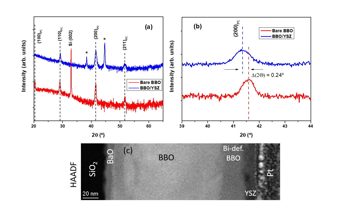
Figure 1(a) shows X-ray diffraction spectra recorded for both bare and capped BBO films. It is found in both cases the presence of peaks corresponding to the BBO perovskite structure while, for capped BBO, YSZ remains amorphous. BBO peaks were indexed considering a pseudo-cubic (PC) lattice. We extracted a cell parameter for bare BBO aPC = 4.339(5) Å, in excellent agreement with the value corresponding to bulk BBO (4.335 Å). Upon YSZ capping, there is a shift of X-ray peaks towards lower angles (see Figure 1(b)), reflecting an (average) BBO unit cell parameter expansion of 0.5%. This is a first indication of the formation of Bi vacancies at the BBO layer, as unit cell enlargement is a signature of B-site vacancies in perovskites Keeble et al. (2013); Brooks et al. (2015); Scafetta and May (2017). We will come back later to this issue.
Figure 1(e) displays a HAADF-STEM cross-section of a capped BBO film. First we notice the existence of a thin BaO layer ( 11 nm, non detectable by XRD) at the substrate/BBO interface, confirmed by the EDS maps displayed at the Suppl. Information SI . This interfacial BaO layer has been observed before in BBO thin films Ferreyra
et al. (2016b) and can be related to the poor sticking coefficient of Bi ions during the first growth stages Li et al. (2019); Zapf et al. (2019). Next, Figure 1(c) displays a BBO layer divided in two zones with different contrast, the darker one ( 30 nm thick) located at the interface with YSZ. As HAADF brightness is higher for species with high atomic number such as Bi, the darker BBO fringe is an indication of Bi-deficiency at this zone. We notice that it is difficult to perform a precise composition quantification, as during EDS mapping we observed some grain growth together with changes in the HAADF contrast between BBO and Bi-deficient BBO SI , indicating atomic diffusion during the measurement. With this constraint in mind, we can roughly estimate a lower bound of 8-10% of Bi vacancies at the Bi-deficient BBO layer SI . This statement is supported from the analysis of (200)PC X-ray peaks performed in the Suppl. Information SI . The (200)PC reflection of bare BBO can be fitted with a single Gaussian component, centered at 2 = 41.59 º, corresponding to a bulk-like cell parameter 4.339(5) Å. On the other hand, the capped BBO (200)PC reflection shows a broadened peak with a slight asymmetry. The peak can be deconvoluted by assuming two Gaussian contributions centered at 2 = 41.59 º and 2 = 41.25 º. These two components are attributed to BBO and Bi-deficient BBO, with cell parameters 4.339(5) Å and 4.374(5) Å, respectively. The latter cell parameter accounts for a 4 pm BBO cell expansion due to the presence of Bi-vacancies. We recall that in the case of Ti deficient SrTiO3 such expansion corresponds to a 10-15% B-cation deficiency Keeble et al. (2013), allowing an additional estimation of the amount of B-site vacancies in the Bi-deficient layer of capped BBO, which is consistent with the previous one obtained from microscopy analysis.
Now we will focus on the electrical transport properties of our samples. BBO single crystals were reported to display an insulating, thermally activated behavior Sleight (2015). Transport properties in BBO thin films have been rarely published: some authors reported an ”insulating behavior” Inumaru et al. (2008) in BBO thin films on MgO but no temperature dependent resistivity was shown, while a negative resistance coeficent, in the range 200-300 K, was displayed for BBO films on silicon Ferreyra et al. (2016a). We recall that the transport properties in semiconducting oxide thin films can be highly affected by the presence of defects. For instance, BaSnO3 thin films were shown to present dramatic changes in their resistivity values -and the corresponding temperature behavior- depending on the films’ free carriers concentration Prakash et al. (2016), strongly linked to the type and number of existing defects.
Electrical transport has been measured on the deposited structures at low temperatures (50-200 K) in a 4-point configuration using a multipurpose Quantum Design Versalab criostat. In order to gain electrical access to the capped BBO samples, we have covered some parts of the substrate by shadows masks during the deposition (Figure 2(b)). Electrical contacts were fixed with silver paste. Figure 2(c) displays the evolution of the 4-points resistance versus temperature for both uncapped and capped BBO films. Bare BBO films show a resistance nearly independent of the temperature -in the measured temperature range-, indicating that the expected thermally activated behavior (negative resistance coefficient) is compensated with a reduction of carriers mobility as temperature increases. We note that the mentioned behavior of the mobility with temperature implies that mobility is limited by phonons rather than by impurity scattering, this balance being very sensitive to free carriers density Zhao et al. (2016). On the other hand, capped BBO shows lower resistance values -a 6-fold decrease at 175 K- together with a semiconducting-like behavior characterized by a decrease of the resistance as the temperature increases. We checked in separated control experiments that both SiO2 and YSZ present resistances several orders of magnitude higher than those shown in Figure 2(c) and this is also the case for the estimated resistance corresponding to the BaO layer ( 10 G), given its reported resistivity ( 104 cm at 700 ºC) and semiconducting-like temperature behavior Dolloff (1956). Therefore we can safely exclude the contribution of these three layers to the electrical transport and assume that, for capped BBO, the electrical transport flows trough two parallel channels related to BBO and Bi-deficient BBO layers (see the sketch of Figure 2(a)). This scenario was considered to fit the experimental data by proposing an equivalent circuit formed by a temperature independent resistance RBBO for the BBO layer in parallel with a polaronic transport channel, attributed to the Bi-deficient BBO layer, with a temperature dependent resistance RPol(T) given by Jaime et al. (1997)
| (1) |
where kB is the Boltzmann constant, T is the absolute temperature, is the electronic charge, is the polaron hopping distance, is the jump attempt frequency -related to the phonon vibrations coupled to the polaron-, Eσ is the activation energy for polaron hopping, gd is an adimensional factor that depends on the hopping geometry111gd=, where is the available sites for a jump, is the defect concentration and was defined in the text. See for instance Ref. 57. and K0=L/Wt, with L, W and t being the length, width and thickness of the Bi-deficient BBO layer, respectively.
The R(T) for the bilayer is thus given by
| (2) |
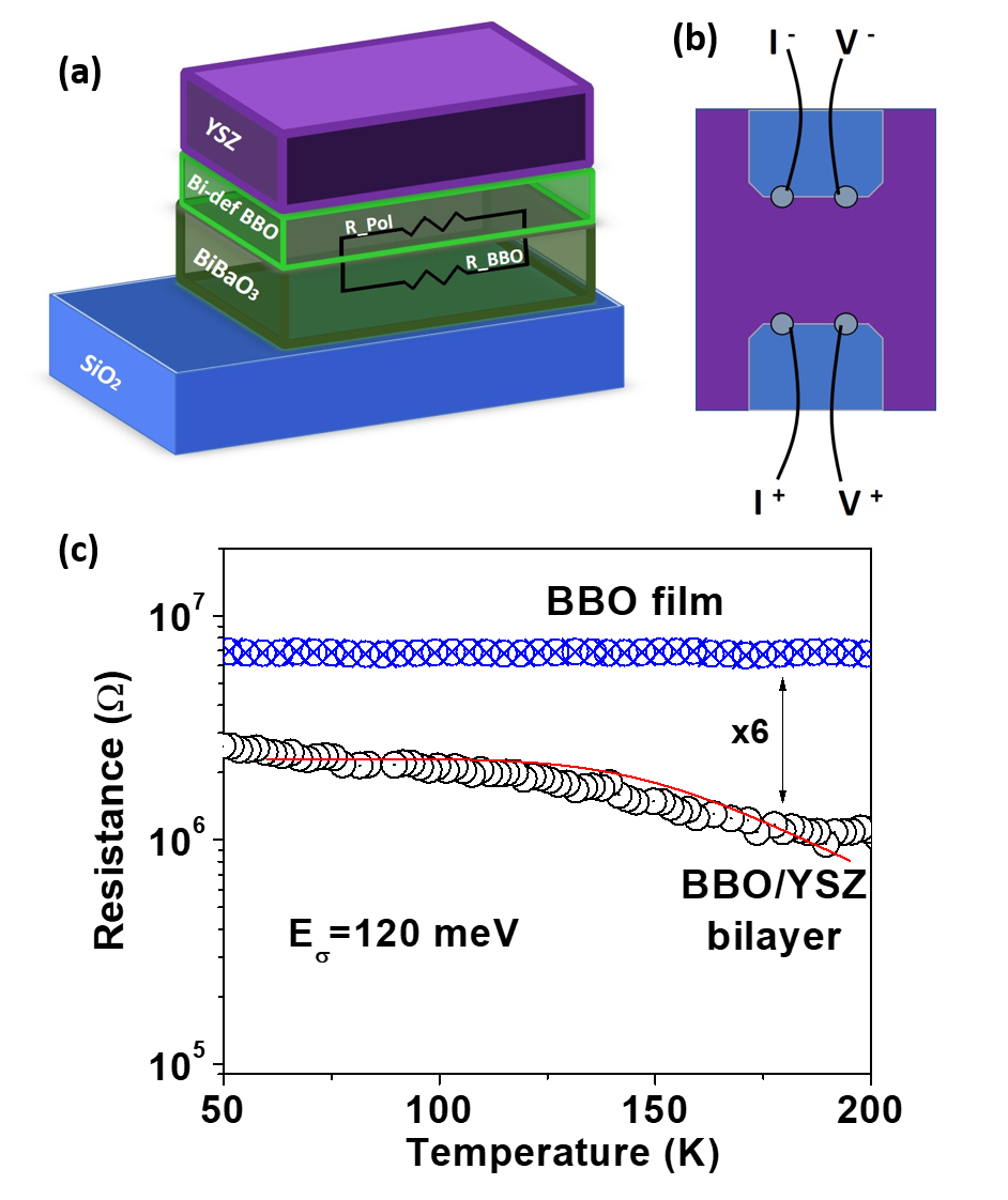
The fitting of R(T) is shown with a red full line in Figure 2(c) and displays a reasonable agreement with the experimental data for Eσ=0.12 eV and .
If we take =1.71013 Hz (the breathing mode vibration frequencySugai et al. (1985)) , a=0.437nm -corresponding to this perovskite cell parameter-, gd=3/8 222gd=3/8 taking N equal to 6 and is estimated considering 1 polaron in the supercell of volume . and =0.067 nm-1 (L/W2 given by our sample geometry and t=30 nm, as extracted from the TEM analysis of Figure 1) we obtain a theoretical value , in very good agreement with the fitted value, giving consistency to our analysis.
We recall that it has been theoretically proposed that, upon hole doping, BBO remains insulating due to the coupling between holes and phonons Franchini et al. (2009) and the subsequent formation of polarons. This is likely the case of Bi-deficient BBO, where the holes for polaron formation are provided by Bi vacancies, as it will be analyzed in the next section by means of first principles calculations.
III DFT calculations
To study the different physical mechanisms that could trigger the transport properties of Bi-deficient BaBiO3, we perform ab initio calculations within the framework of Density Functional Theory (DFT) and the projector augmented wave (PAW) method Blöchl (1994), as implemented in the Vienna ab initio package (VASP) Kresse and Furthmüller (1996); Kresse and Joubert (1999). We explicitly treat 10 valence electrons for Ba (5s25p66s2), 15 for Bi (5d106s26p3) and 6 for O (2s22p4).
To properly describe the electronic structure of charge ordered and semiconducting BaBiO3 -specially in the presence of localized defects-, it is necessary to consider long range exchange interactions that are poorly described by the standard local and semilocal functionals as the local density approximation (LDA) or the general gradient approximation (GGA). Therefore, we use the semilocal functionals developed by Perdew, Burke and Ernzerhof (PBE) Perdew et al. (1996) and we add the hybrid functional including a fraction of non-local Hartree-Fock exchange interactions through the Heyd-Scuseria-Ernzerhof (HSE06) functionals Heyd et al. (2003); Krukau et al. (2006) in all the calculations.
The charge-ordered phase of BaBiO3 is represented formally by the BaBi+3Bi+5O formula unit. The two Bi species are ordered in an alternated way within a monoclinic structure Cox and Sleight (1976b). To compute the electronic properties of perfect BaBiO3 and Bi-deficient BaBi0.75O3, containing a 25 of Bi-vacancies, we use a supercell rotated 45∘ with respect to the simple cubic single perovskite and which contains 4 Bi sites in total, 2 per layer and two planes in the -direction. To explore lower concentrations of Bi-vacancies we also perform calculations in a 2x2x2 FCC supercell containing 80 atoms 333To build this FCC supercell we begin with a 2x2x2 supercell of the simple cubic perovskite containing 40 atoms in total and we perform several molecular dynamics steps, followed by relaxation, to stabilize the breathing distortion driven by the charge disproportionation. Once this distortion agree well with the experimental one, we build up again a 2x2x2 supercell, described within the FCC Bravais lattice., as the one used in Ref. Franchini et al., 2009. This larger supercell contains 16 Bi-atoms per unit cell and we account for defect concentrations of 12.5 (2 Bi-vacancies) and 18.75 (3 Bi-vacancies).
The HSE calculations within the smaller unit cell are performed using a 450 eV energy cutoff in the plane waves basis and to evaluate the integrals within the Brillouin Zone (BZ), a 443 Monkhorst-Pack -point grid is employed. The corresponding values for the energy cutoff and -points grid in the larger FCC supercell are 400 eV and 222, respectively. The experimental lattice parameters Cox and Sleight (1976b) are used in all the calculations and internal structural relaxations are performed until the forces on each ion are less than 0.02 eV/Å.
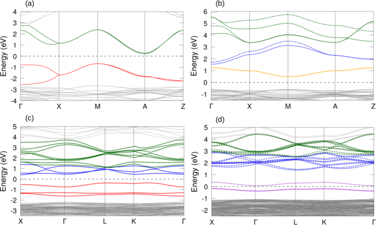
For perfect BaBiO3, our calculations predict the semiconducting state with a band gap of 0.90 eV, exhibiting the charge disproportionation between the two different species, Bi+3 and Bi+5 in agreement with previous calculations Franchini et al. (2010). In Figure 3(a) we show the corresponding bandstructure where the full 6s bands of Bi+3 are depicted in red and the empty ones of Bi+5 are in dark green. It is important to mention that the Bi-O bonds can be described by spatially extended hybridized 6s-2p orbitals and all the bands present a strong s-p hybridization. The color coding used in Figure 3 and in the following ones is just a guide to the eye.
Distinct kinds of defects appear in the presence of Bi vacancies. It is worth to mention that several molecular dynamics steps, followed by relaxation, were necessary to stabilize these defects in order to avoid spurious metallic solutions Franchini et al. (2009). In the following, we describe the results obtained for the different Bi vacancies concentrations considered.
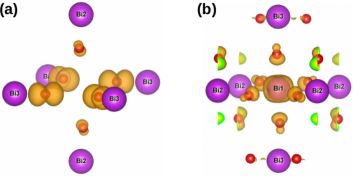
The system with 25 of Bi vacancy concentration has been simulated in the small cell where one out of four Bi is withdrawn. Independently of the site of the vacancy, whether it is at a Bi+5 or Bi+3 site, the resulting electronic structure is very similar. For instance, if the vacancy is at a Bi+5 site, in order to compensate the lacking five electrons, each of the remaining two Bi+3 liberates two electrons, so that the originally full 6s bands become empty. These two trapped holes at each form a bipolaron. Since the remaining Bi+5 site has its 6s band already empty, the other missing electron turns into a hole trapped at the surrounding oxygen cloud next to the Bi vacancy. On the other way around, if the vacancy is at a Bi+3 site, the lacking three electrons give rise to a bipolaron at the remaining Bi+3 site and a hole trapped at the oxygen p-bands surrounding the vacancy. In Figure 3 (b) we show the electronic bandstructure, with the orange narrow band corresponding to holes trapped at the oxygen cloud around the vacancy, whose charge density is depicted in Figure 4(a). The bands in blue are the bipolarons with the corresponding charge density shown in Figure 4(b).
As mentioned before, the system with 12.5 and 18.5 Bi vacancy concentrations has been simulated with a supercell containing 16 Bi sites. In the case with an even amount of vacancies, the kind of electronic defects are only of the bipolaron type.
In Figure 3 (c), we show the calculated electronic bandstructure obtained for the 12.5 concentration, where there are two vacancies at Bi+3 sites in the unit cell. The three occupied bands in red are the full 6s bands of the remaining Bi+3, the three bands in blue are those of the bipolarons, and, at higher energies, the eight 6s bands of the Bi+5 are in dark-green. In the case of even number of vacancies, the system is non-spin polarized so that the bands are doubly degenerate.
When the Bi vacancy concentration is 18.75 , there are three vacancies in the supercell. For example, if two of the vacancies are at a Bi+3 site and the other one at a Bi+5, there are eleven electrons missing. The six remaining Bi+3 sites can provide this charge. That is, five of these Bi+3 sites turn into Bi+5 by trapping two holes each giving rise to five bipolarons (blue bands in Figure 3 (d)). The remaining Bi+3 keeps one electron forming a polaron with a localized spin-polarized charge (violet band in Figure 3 (d)).
In order to analyse the role played by each type of defects into the transport properties we proceed to estimate the activated diffusion barrier Eσ in each case.
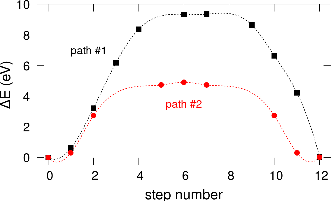
The hole polaron trapped at the -bands of the oxygens that surround the Bi vacancy in the highly doped case (25 vacancy concentration), is a mixed type of defect where the Bi vacancy is bound to a hole electronic cloud. Nudged elastic bands (NEB)Henkelman and Jónsson (2000) method has been used to estimate the activation barrier, taking into account two different migration pathways. The first one considers the migration of the defect within the -plane, that is in the plane that contains the part of the hole shared by the 4 in-plane oxygen atoms. The second considered path was with the defect travelling along the (111)-() direction, with the inflection point located at an optimized height. That is, the defect travelling from the (1/2,1/2,1/2) to the (0,0,0) position, through (1/4,1/4,h0), being h0 the optimized distance in the -direction from the -plane. We obtain Eσ=9.35 eV and 4.9 eV, respectively. In view of these results, we conclude that the contribution to the electronic conductivity of these type of mixed defects is negligible.
To estimate the maximun of the energy barrier of the polaron and bipolaron trapped at Bi+3 sites (violet and blue bands of Figure 3, respectively), we perform a static calculation where the lattice distortion coupled to the defect is transferred to an intermediate situation that forces the trapped charge to be shared between neighboring Bi sites.
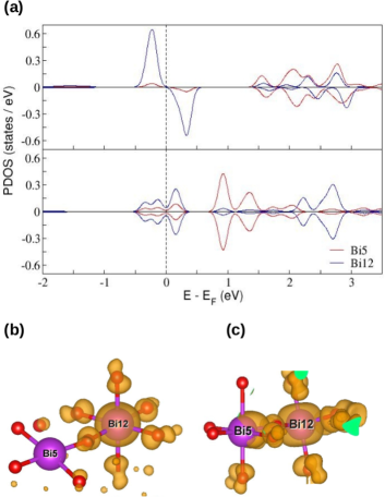
For the case with 18.75 Bi vacancy concentration, in the top panel of Figure 6 (a), we show the partial density of states (PDOS) projected onto the s-orbitals of two Bi neighboring sites, one of them trapping the polaron (labeled as Bi12) and the other one belongs to a Bi+5, named Bi5. The corresponding charge density associated with the polaron is shown in Figure 6 (b). In the bottom panel of Figure 6 (a), we plot the PDOS projected on the same Bi sites but in the situation where the polaron charge is shared in equal parts between them. In Figure 6 (c) we show the related charge density. The energy difference between the initial and the intermediate situation provides an estimation of Eσ, that is 0.54 eV. When this approach is done to estimate Eσ for the bipolaron migration, where now two holes are hopping simultaneously, we obtain Eσ=0.60 eV.
Interestingly, it is not surprising that this energy scale is related to the electron-phonon coupling in BBO systems, specially with the breathing phonon modes that are strongly correlated to Bi+5- Bi+3 charge ordering. The value around 0.5 eV for Eσ is of the same order of magnitude as the energy shift induced in the electronic bands when frozen phonon pertubations for the breathing mode are performed for bulk BBOYin et al. (2013). However, as it has been recently reported in Ref. 21, this value decreases to 0.2 eV in confined situations as the one described for the BBO/BaPbO3 interface. So, it is likely that the value of 0.5 eV obtained for the bulk supercell described here is overestimated since it does not take into account the confinement effects present in the real samples. Therefore, we consider that the actual activation energy might be close to the 0.12 eV obtained from the transport experiments and that the migration of polarons trapped at Bi+3 sites plays an important role in the increment of the electrical conductivity with the temperature, experimentally observed in our Bi deficient films.
The existence of polarons or bipolarons trapped at Bi sites in BBO was already theoretically described in Ref. 46. The difference is that in that work the doping is caused by K substitution at Ba sites. They show that local lattice relaxations are sufficiently large to screen the localized holes and that hole doped BBO remains semiconducting upon moderate hole doping. In our work, we show that the level of doping with Bi vacancies is 3 to 5 times larger than with K. Notwithstanding this, it is remarkable that the system remains semiconducting for all the concentrations studied.
IV Conclusions
We have shown that it is possible to synthesize thin layers of BBO perovskite with a large amount of Bi-vacancies. Transport properties were modelled with a polaronic model and the existence of these defects was theoretically validated. Our DFT calculations performed for Bi-deficient BBO supercells show that Bi vacancies give rise to different type of polarons, depending on the vacancies concentration. After the Bi vacancy is formed, the missing electrons induce polaron and/or bipolarons that consist in one or two holes trapped at some of the remaining Bi sites, or even at the oxygen octahedron surrounding the vacancy for large vacancies concentrations.
We conclude that hole doped BBO remains semiconducting despite the large hole concentration induced by the Bi deficiency. We finally estimate the activated diffusion barrier for all these type of defects to analyse their contribution to the transport properties. We show that the calculated energy barriers of the charges trapped at Bi sites are correlated to the electron-phonon coupling energy scale. The calculated activated barriers for the simulated bulk supercells are somewhat larger than the one obtained from the fit of the transport experiments. In view of previous theoretical results for other BBO interfaces, these larger values are expected to decrease in confined situations -such as the Bi-deficient BBO layer studied in this work- and match the experimentally extracted activation energies. We finally conclude that the polarons trapped at Bi sites strongly contribute to the electrical conductivity of Bi-deficient BBO and, in a more general framework, that the control of Bi vacancies can be used as a tool for tuning the electronic properties of this perovskite.
V Acknowledgments
The authors received financial support from PICTs 2015-0869, 2016-0867, 2017-1836 and 2019-02128 of ANPCyT, Argentina. Also, funding from EU-H2020-RISE project ”MELON” (SEP-2106565560) is acknowledged. DR thanks the Nederlandse Organisatie voor Wetenschappelijk Onderzoek for a visiting grant, project 040.11.735, ”Memcapacitive elements for cognitive devices”. We thank D. Vega, from CAC-CNEA, for some of the XRD measurements.
References
- Coey et al. (2009) J. Coey, M. Viret, and S. von Molnár, Advances in Physics 58, 571 (2009).
- Dawber et al. (2005) M. Dawber, K. M. Rabe, and J. F. Scott, Rev. Mod. Phys. 77, 1083 (2005).
- Rao (1990) C. N. R. Rao, Ferroelectrics 102, 297 (1990).
- Shellaiah and Sun (2020) M. Shellaiah and K. W. Sun, Chemosensors 8, 55 (2020).
- Sawa (2008) A. Sawa, Materials Today 11, 28 (2008).
- Yu (2017) S. Yu, Neuro-inspiring computing using resistive synaptic devices (Springer International Publishing, 2017).
- Gunkel et al. (2020) F. Gunkel, D. V. Christensen, Y. Z. Chen, and N. Pryds, Appl. Phys. Lett. 116, 120505 (2020).
- Rose et al. (2021) M.-A. Rose, B. Šmíd, M. Vorokhta, I. Slipukhina, M. Andrä, H. Bluhm, T. Duchoň, M. Ležaić, S. A. Chambers, R. Dittmann, et al., Advanced Materials 33, 2004132 (2021).
- Mattheiss et al. (1988) L. F. Mattheiss, E. M. Gyorgy, and D. W. Johnson, Phys. Rev. B 37, 3745 (1988).
- Cava et al. (1988) R. J. Cava, B. Batlogg, J. J. Krajewski, R. Farrow, L. W. Rupp Jr, A. E. White, K. Short, J. F. Peck, and T. Kometani, Nature 332, 814 (1988).
- Cox and Sleight (1976a) D. Cox and A. Sleight, Solid State Communications 19, 969 (1976a).
- Kennedy et al. (2006) B. J. Kennedy, C. J. Howard, K. S. Knight, Z. Zhang, and Q. Zhou, Acta Crystallographica Section B 62, 537 (2006).
- Shen et al. (1989) Z.-X. Shen, P. A. P. Lindberg, B. O. Wells, D. S. Dessau, A. Borg, I. Lindau, W. E. Spicer, W. P. Ellis, G. H. Kwei, K. C. Ott, et al., Phys. Rev. B 40, 6912 (1989).
- Nagoshi et al. (1992) M. Nagoshi, T. Suzuki, Y. Fukuda, K. Ueki, A. Tokiwa, M. Kiruchi, Y. Syono, and M. Tachiki, Journal of Physics: Condensed Matter 4, 5769 (1992).
- Foyevtsova et al. (2015) K. Foyevtsova, A. Khazraie, I. Elfimov, and G. A. Sawatzky, Phys. Rev. B 91, 121114 (2015).
- Plumb et al. (2016) N. C. Plumb, D. J. Gawryluk, Y. Wang, Z. Ristić, J. Park, B. Q. Lv, Z. Wang, C. E. Matt, N. Xu, T. Shang, et al., Phys. Rev. Lett. 117, 037002 (2016).
- Balandeh et al. (2017) S. Balandeh, R. J. Green, K. Foyevtsova, S. Chi, O. Foyevtsov, F. Li, and G. A. Sawatzky, Phys. Rev. B 96, 165127 (2017).
- Yan et al. (2013) B. Yan, M. Jansen, and C. Felser, Nature Phys. 9, 709 (2013).
- Vildosola et al. (2013) V. Vildosola, F. Güller, and A. M. Llois, Physical Review Letters 110, 206805 (2013).
- Meir et al. (2017) B. Meir, S. Gorol, T. Kopp, and G. Hammerl, Phys. Rev. B 96, R100507 (2017).
- Di Napoli et al. (2021) S. Di Napoli, C. Helman, A. M. Llois, and V. Vildosola, arxiv: 2011.08710 (2021).
- Makita and Abe (1997) T. Makita and H. Abe, Japanese Journal of Applied Physics 36, L96 (1997).
- Gozar et al. (2007) A. Gozar, G. Logvenov, V. Y. Butko, and I. Bozovic, Phys. Rev. B 75, 201402 (2007).
- Inumaru et al. (2008) K. Inumaru, H. Miyata, and S. Yamanaka, Phys. Rev. B 78, 132507 (2008).
- Lee et al. (2016) H. G. Lee, Y. Kim, S. Hwang, G. Kim, T. D. Kang, M. Kim, M. Kim, and T. W. Noh, APL Materials 4, 126106 (2016).
- Ferreyra et al. (2016a) C. Ferreyra, F. Guller, F. Marchini, U. Lüders, C. Albornoz, A. G. Leyva, F. J. Williams, A. M. Llois, V. Vildosola, and D. Rubi, AIP Advances 6, 065310 (2016a).
- Ferreyra et al. (2016b) C. Ferreyra, F. Marchini, P. Granell, F. Golmar, C. Albornoz, F. Williams, A. Leyva, and D. Rubi, Thin Solid Films 612, 369 (2016b).
- Zapf et al. (2018) M. Zapf, M. Stübinger, L. Jin, M. Kamp, F. Pfaff, A. Lubk, B. Büchner, M. Sing, and R. Claessen, Applied Physics Letters 112, 141601 (2018).
- Zapf et al. (2019) M. Zapf, S. Elsässer, M. Stübinger, P. Scheiderer, J. Geurts, M. Sing, and R. Claessen, Phys. Rev. B 99, 245308 (2019).
- Bouwmeester et al. (2019) R. L. Bouwmeester, K. de Hond, N. Gauquelin, J. Verbeeck, G. Koster, and A. Brinkman, physica status solidi (RRL) 13, 1800679 (2019).
- Jin et al. (2020) L. Jin, M. Zapf, M. Stübinger, M. Kamp, M. Sing, R. Claessen, and C.-L. Jia, physica status solidi (RRL) 14, 2000054 (2020).
- Kim et al. (2015) G. Kim, M. Neumann, M. Kim, M. D. Le, T. D. Kang, and T. W. Noh, Phys. Rev. Lett. 115, 226402 (2015).
- Skinner and Kilner (2003) S. J. Skinner and J. A. Kilner, Materials Today 6, 30 (2003).
- Kilo et al. (2000) M. Kilo, G. Borchardt, B. Lesage, O. Kaïtasov, S. Weber, and S. Scherrer, Journal of the European Ceramic Society 20, 2069 (2000).
- (35) See Supplemental Material at (link) for additional X-ray diffraction and TEM experiments (????).
- Keeble et al. (2013) D. J. Keeble, S. Wicklein, L. Jin, C. L. Jia, W. Egger, and R. Dittmann, Phys. Rev. B 87, 195409 (2013).
- Brooks et al. (2015) C. M. Brooks, R. B. Wilson, A. Schäfer, J. A. Mundy, M. E. Holtz, D. A. Muller, J. Schubert, D. G. Cahill, and D. G. Schlom, Applied Physics Letters 107, 051902 (2015).
- Scafetta and May (2017) M. D. Scafetta and S. J. May, Phys. Chem. Chem. Phys. 19, 10371 (2017).
- Li et al. (2019) F. Li, B. A. Davidson, R. Sutarto, H. Shin, C. Liu, I. Elfimov, K. Foyevtsova, F. He, G. A. Sawatzky, and K. Zou, Phys. Rev. Materials 3, 100802 (2019).
- Sleight (2015) A. W. Sleight, Phys. C 514, 152 (2015).
- Prakash et al. (2016) A. Prakash, P. Xu, A. Faghaninia, S. Shukla, J. W. Ager, C. S. Lo, and B. Jalan, Nature Commun. 8, 15167 (2016).
- Zhao et al. (2016) T. Zhao, W. Shi, J. Xi, D. Wang, and Z. Shuai, Sci. Reports 6, 19968 (2016).
- Dolloff (1956) R. T. Dolloff, Journal of Applied Physics 27, 1418 (1956).
- Jaime et al. (1997) M. Jaime, H. T. Hardner, M. B. Salamon, M. Rubinstein, P. Dorsey, and D. Emin, Phys. Rev. Lett. 78, 951 (1997).
- Sugai et al. (1985) S. Sugai, S. Uchida, K. Kitazawa, S. Tanaka, and A. Katsui, Phys. Rev. Lett. 55, 426 (1985).
- Franchini et al. (2009) C. Franchini, G. Kresse, and R. Podloucky, Phys. Rev. Lett. 102, 256402 (2009).
- Blöchl (1994) P. Blöchl, Phys. Rev. B 50, 17953 (1994).
- Kresse and Furthmüller (1996) G. Kresse and J. Furthmüller, Phys. Rev. B 54, 11169 (1996).
- Kresse and Joubert (1999) G. Kresse and D. Joubert, Phys. Rev. B 59, 1758 (1999).
- Perdew et al. (1996) J. Perdew, S. Burke, and M. E. M, Phys. Rev. Lett. 77, 3865 (1996).
- Heyd et al. (2003) J. Heyd, G. E. Scuseria, and M. Ernzerhof, The Journal of Chemical Physics 118, 8207 (2003).
- Krukau et al. (2006) A. V. Krukau, O. A. Vydrov, A. F. Izmaylov, and G. E. Scuseria, The Journal of Chemical Physics 125, 224106 (2006).
- Cox and Sleight (1976b) D. Cox and A. Sleight, Solid State Communications 19, 969 (1976b).
- Franchini et al. (2010) C. Franchini, A. Sanna, M. Marsman, and G. Kresse, Phys. Rev. B 81, 085213 (2010).
- Henkelman and Jónsson (2000) G. Henkelman and H. Jónsson, J. Chem. Phys. 113, 9901 (2000).
- Yin et al. (2013) Z. P. Yin, A. Kutepov, and G. Kotliar, Physical Review X 3 (2013).
- Tilley (2008) R. J. D. Tilley, Defects in solids (John Wiley & Sons, Inc, 2008).