Imaging the Néel vector switching in the monolayer antiferromagnet MnPSe3 with strain-controlled Ising order
The family of monolayer two-dimensional (2D) materials hosts a wide range of interesting phenomena, including superconductivity costanzonatnano16 , charge density waves xinatnano15 , topological states wuscience18 and ferromagnetism huangnat17 , but direct evidence for antiferromagnetism in the monolayer has been lacking maknatrevphys19 . Nevertheless, antiferromagnets have attracted enormous interest recently in spintronics due to the absence of stray fields and their terahertz resonant frequency nvemecnatphys18 . Despite the great advantages of antiferromagnetic spintronics, controlling and detecting Néel vectors have been limited in bulk materials wadleyscience16 ; saidlnatphot17 ; nvemecnatphys18 ; cheongnpj20 ; nairnatmat20 . In this work, we developed a sensitive second harmonic generation (SHG) microscope and detected long-range Néel antiferromagnetic (AFM) order and Néel vector switching down to the monolayer in MnPSe3. Temperature-dependent SHG measurement in repetitive thermal cooling surprisingly collapses into two curves, which correspond to the switching of an Ising type Néel vector reversed by the time-reversal operation, instead of a six-state clock ground state expected from the threefold rotation symmetry in the structure oshikawaprb00 ; louprl07 ; cheongnpj19 . We imaged the spatial distribution of the Néel vectors across samples and rotated them by an arbitrary angle irrespective of the lattice in the sample plane by applying strain. By studying both a Landau theory and a microscopic model that couples strain to nearest-neighbor exchange, we conclude that the phase transition of the XY model in the presence of strain falls into the Ising universality class instead of the XY one, which could explain the extreme strain tunability. Finally, we found that the 180∘ AFM domain walls are highly mobile down to the monolayer after thermal cycles, paving the way for future control of the antiferromagnetic domains by strain or external fields on demand for ultra-compact 2D AFM terahertz spintronics.
Detection and control of the spin order in ferromagnetic materials is the main principle in current information technology. The discovery of 2D ferromagnetic materials using the polar Kerr effect huangnat17 ; gongnat17 has triggered tremendous interest in studying magnetism in the true 2D limit dengnat18 ; feinatmat18 ; thielsci19 ; chensci19 and spintronic device applications in van der Waals heterostructure materials songsci18 ; kleinsci18 ; wangnatcomm18 ; huangnatnano18 ; jiangnatmat18 ; jiangnatnano18 . Optical techniques are powerful tools to detect magnetism maknatrevphys19 , but clear evidence for the AFM order in atomically thin 2D crystals has not been identified due to the lack of sensitive direct detection. The polar Kerr effect is absent in AFM materials when the total magnetization is zero burchnat18 ; gongsci19 ; maknatrevphys19 ; gibertininatnano19 . Although Raman spectroscopy is a powerful tool to study spin-phonon coupling and collective magnons leenanolett16 ; wang2Dmat16 ; kim2dmat19 ; vaclavkova2dmat20 , their identification often do not provide unambiguous identification of the AFM order maknatrevphys19 ; huangnatmat2020 . Non-optical methods such as tunneling magneto-resistance measurement have indicated the correlation in the monolayer of an AFM materiallongnanoletter20 , but it is also not a direct probe of the AFM order parameter maknatrevphys19 ; huangnatmat2020 . SHG has been shown to be a sensitive tool to detect AFM orders due to inversion symmetry breaking from the spin order in magneto-electric materials including bulk Cr2O3 fiebigreview05 , few-layer MnPS3 chuprl20 and a synthetic bilayer CrI3 sunnat19 . Nevertheless, the detection of intrinsic AFM in the monolayer has not been demonstrated yet, which remains an unresolved fundamental question and is also not ideal for AFM terahertz spintronics at the smallest scales. In this work, we systematically study the layer-dependent AFM order, Néel vector distribution, switching and its strain tunability in a 2D crystal of MnPSe3 wiedenmannssc81 by a newly developed sensitive SHG imaging microscope. (See methods.)
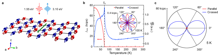
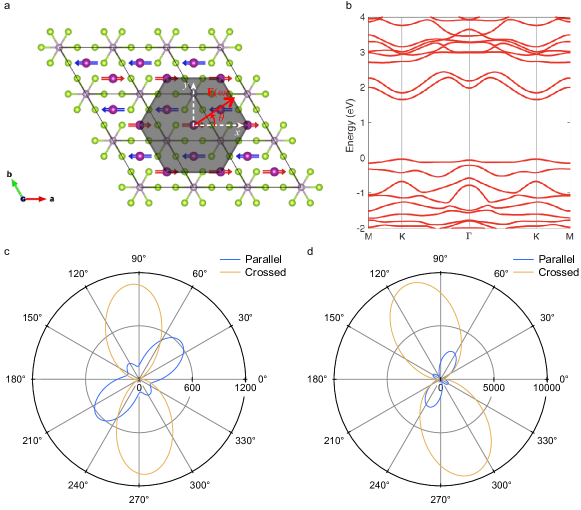
MnPSe3 belongs to the family of AFM transition metal phosphorous trichalcogenide MPX3 (M = Mn, Ni, Fe, Co, X = S, Se), among which Mn compounds form inversion-breaking Néel order while others are in centrosymmetric Zigzag ordered phases wiedenmannssc81 ; wildesjpcm98 ; wildesjpcm12 ; wildesprb15 ; ressoucheprb10 ; lancconprb16 . In contrast to MnPS3, which has dominant out-of-plane moments jeevanandamjpcm1999 ; ressoucheprb10 , MnPSe3 has in-plane spins with very large XY anisotropy according to the neutron scattering measurement wiedenmannssc81 (Fig. 1a), which offers richer magnetic domain structures such as vortices and tunability cheongnpj19 . Above the Néel temperature, , MnPSe3 belongs to the point group and space group 148 wiedenmannssc81 , and has an inversion center between two neighboring Mn atoms but no mirror symmetry. The Mn atoms form a honeycomb lattice in one layer (Fig. 1a), and the honeycomb layers form the rhombohedral (ABC) stacking along the axis with a threefold rotational symmetry. Different from FePS3 and NiPS3, which have a change of twofold rotational symmetry in the bulk to a threefold rotational symmetry in the monolayer leenanolett16 ; wang2Dmat16 ; kimnatcomm19 ; kangnat2020 , MnPSe3 is always three-fold symmetric. As shown in the inset of Fig. 1b, a small temperature-independent SHG from the electric quadruple (EQ) contribution, follows the lattice threefold rotational symmetry above . (See methods.) The parallel and crossed configuration correspond to and respectively while we co-rotate and by 360∘ in the plane wunatphys17 . Below the Néel temperature, the formation of the Néel AFM order with in-plane spins breaks the inversion symmetry (), which allows electric dipole (ED) contribution to the SHG, fiebigreview05 . is proportional to the order parameter, the Néel vector , savalenti00 and changes the sign when flips by 180∘ (, where and are the magnetization of two neighboring Mn atoms). (See Fig. 1a). In the AFM state, the product of the inversion symmetry () and the time-reversal symmetry (), so called symmetry, is still preserved lipnas13 , even though both and are broken. This kind of ED term is often called non-reciprocal or c-type SHG allowed by the symmetry, while the EQ term is an i-type SHG, where ‘c’ and ‘i’ mean changing and invariant under time-reversal symmetry respectively fiebigreview05 . Fig. 1b shows a typical SHG response as a function of temperature on a 100-nm thick flake exfoliated on SiO2/Si. A sharp turn-on of the ED SHG signal clearly indicates a phase transition at 67.9 0.2 K, agreeing well with the (68 0.5 K) determined from in-plane magnetization measurement. Below , as shown in Fig. 1c, a giant twofold signal emerges in the crossed configuration, which clearly breaks the threefold rotation symmetry. Another surprising observation is that the peak of the parallel polar pattern is only 1/20 of that in the crossed pattern, which was not observed in previous invariant van der Waals AFM materials sunnat19 ; chuprl20 . The nodal direction of the twofold crossed pattern is also shown to be close to the Néel vector direction (see Supplementary Note 1 and 2).
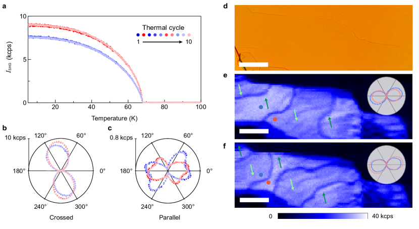
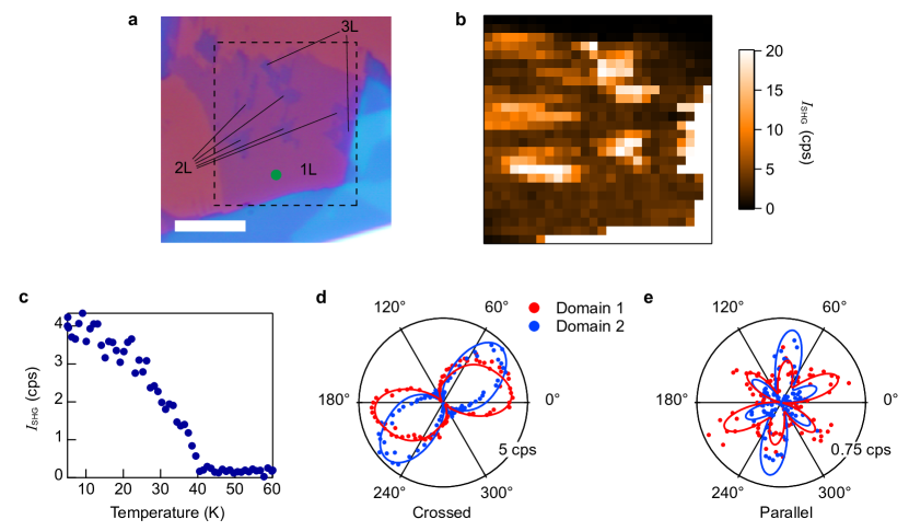
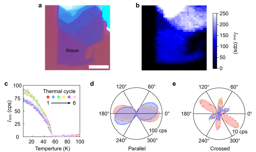
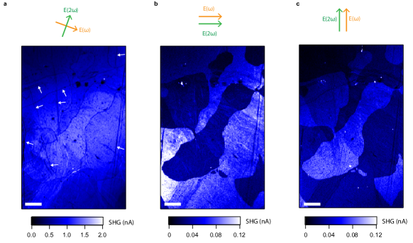
After confirming the detection of AFM order by SHG, we use scanning SHG microscopy with 2 m spatial resolution to study the AFM domains. In MnPSe3 with in-plane spins and large XY anisotropy jeevanandamjpcm1999 ; wiedenmannssc81 , six energetically equal magnetic domains are expected due to the threefold rotational crystalline anisotropy and the time-reversal operation oshikawaprb00 ; louprl07 ; cheongnpj19 . Nevertheless, Fig. 2a shows that temperature-dependent SHG under ten consecutive cooling runs across on the same spot of a 15-m thick sample collapses onto two curves instead of six. The crossed and parallel polar patterns that respond to these two AFM domains are shown in Fig. 2b,c. To figure out the relation between these two domains, we performed spatial scanning SHG microscopy at 5 K with angles of the two polarizers chosen near the maximum signal in the crossed pattern. An optical image of a region with uniform thickness ( 100 nm, a second exfoliated thick sample) and SHG maps at 5 K after two cooling processes across are shown in Fig. 2d-f. Sharp dark lines with very low SHG intensity are observed, with bright domains of high and nearly equal SHG intensity on both sides. In one of the regions, we pick up a few points such as the blue dot in Fig. 2e and observe the same polar patterns shown as blue in the top right of Fig. 2e. Crossing the dark line to a different region, we pick up a few points such as the orange one and observe the crossed polar patterns rotated by a small angle shown as orange on the top right of Fig. 2e. By keeping the laser spot at the orange point and performing a few thermal cycles, the polar pattern switches only between the blue and orange ones shown in Fig. 2e. We interpret the two regions with high SHG intensity as two different AFM domains where the spins are reversed by 180∘ under the time-reversal operation and the dark lines are domain walls due to destructive interference fiebigreview05 ; yinsci2014 . The arrows in Fig. 2e,f indicate the opposite directions of the Néel vectors in different regions determined by SHG polar pattern measurements at 5 K. (See Supplementary Note 1.) A second SHG map after a thermal cycling across in Fig. 2f shows that the domain wall is not pinned and different regions still only have the two kinds of polar patterns shown in 2e. (See the mapping on a 30 m-thick naturally grown sample in Supplementary Figure 6.) The reason why we could observe the domain wall between two AFM regions with a phase shift by the destructive SHG interference is that the SHG has both ED and EQ contributions and only the ED term is sensitive to the phase shift. One could write the signal we observe as , where the signs indicate the sign change of the ED term under time-reversal operation. As shown in Fig. 1b and 2a, the ED contribution at 5 K is 200 times larger than the EQ part and therefore the two AFM domains have high and nearly equal SHG while the domain wall has very low SHG with the EQ contribution only.
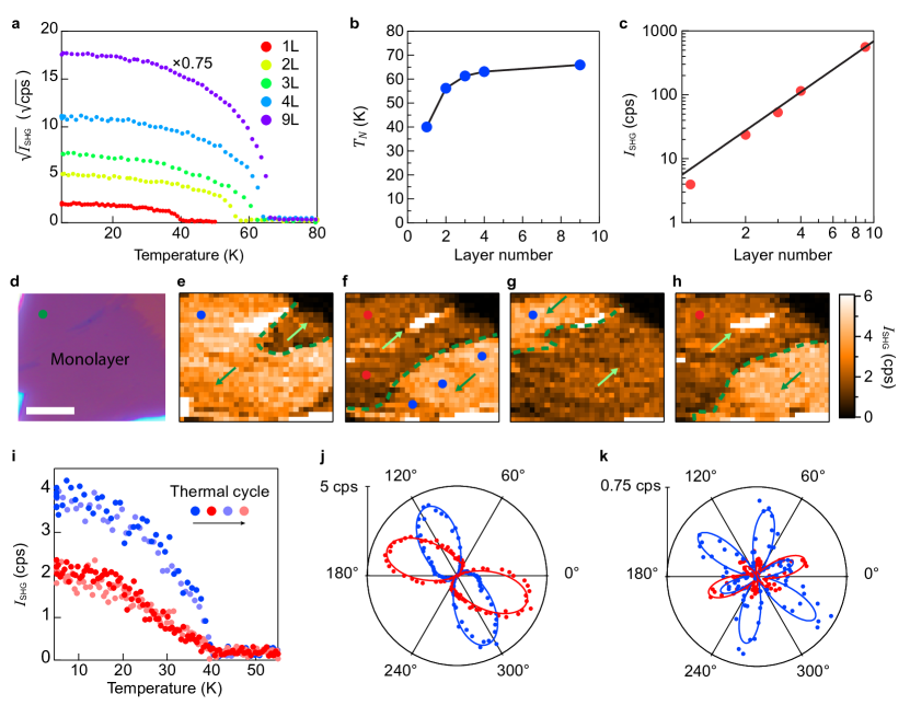
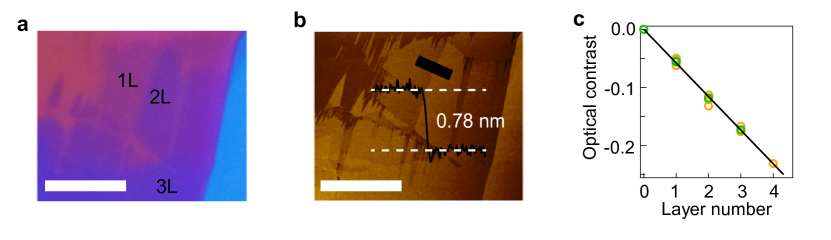
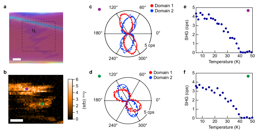
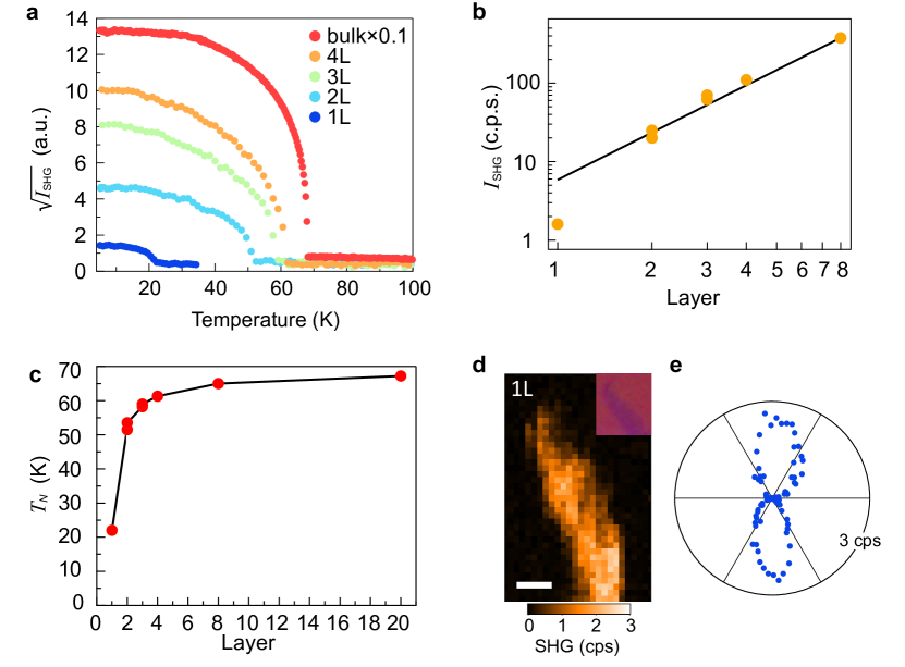
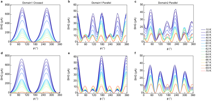
Before we discuss the origin of the two-state Ising order instead of the six-state clock order, we investigate whether the AFM order exists and direct imaging of Néel vector switching could be detected in the monolayer first. The ultra-thin flakes down to the monolayer are exfoliated on SiO2/Si wafers. The number of layers are determined by a combination of atomic force microscopy and optical contrast measurements casiraghinanoletter07 . (See Extended Data Figure 1.) To probe the intrinsic properties of the materials, we exfoliate samples down to the monolayer in a glove box. Fig. 3a shows the layer-dependent square root of the SHG intensity measured as a function of the temperature. All of the thin flakes show a clear phase transition down to the monolayer with the layer-dependent transition temperature shown in Fig. 3b. The transition temperature decreases from 66 K in the nine-layer sample to 56 K in the bilayer sample and it is 40 K measured in three different monolayer samples (see Extended Data Figure 2-3 for the other two monolayer samples). The intensity of SHG at 5 K from 1 layer to 9 layers nearly follows a quadratic dependence on the layer count (Fig. 3c), which is expected for breaking the inversion symmetry in all these samples zhaolight16 ; liusci20 . This is different from synthetic layered AFM CrI3 which supports SHG signals only with even numbers of layers sunnat19 . Fig. 3d shows an optical image of the monolayer MnPSe3 sample 1 (S1). We performed twelve thermal cycles at the green dot shown in Fig. 3d with the temperature-dependent SHG collapsed on two curves, and we plot four of them as examples in Fig. 3i. The corresponding polar patterns for the two AFM states are shown in Fig. 3j,k. Note that the change of the orientation in the crossed patterns in the monolayer is larger than that in bulk samples because of the reduced intensity ratio between the ED and EQ terms with reduced thickness. Fig. 3e-h shows four SHG maps at 5 K after thermal cycles and the green dashed lines are mobile AFM domain walls. All of them exhibit a contrast with two domains, with Fig. 3e showing a dominant bright domain. Measured polar patters on selected dots marked by red and blue in Fig. 3e-h have the same red and blue patterns shown in Fig. 3j,k. (See Extended Data Figure 4 for more data.) We would like to point out that we observed a drop of by 2-4 K in the bilayer and by 18 K in the monolayer due to aging effects when samples are exfoliated in air. (See Extended Data Figure 5.)
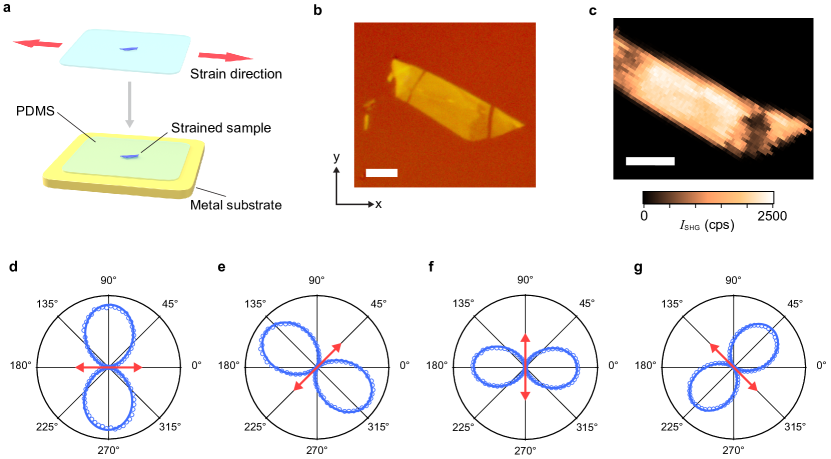
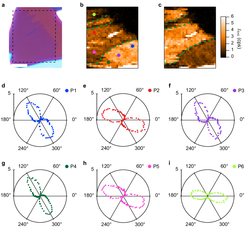
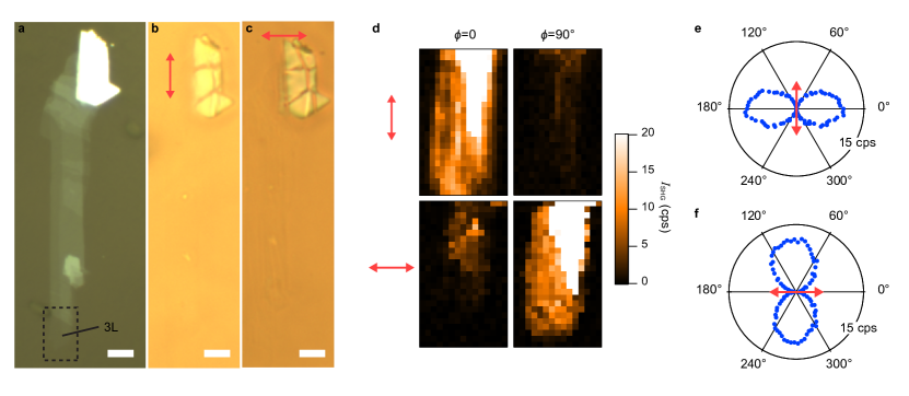
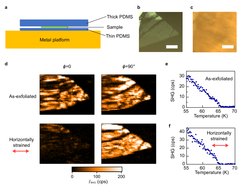
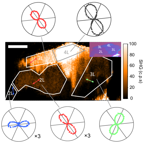
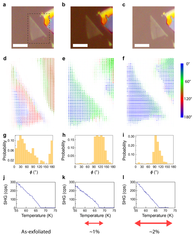
We observed the same two-state Ising order on all of the samples with thickness from monolayer to 30 m either exfoliated on SiO2/Si or directly glued on the metal platform of the cryostat. All of them show two-fold crossed polar patterns, regardless whether they are prepared in air or in a glovebox. (See Extended Data Figure 2-6, Supplementary Figure 2, 4, 7 and 9.) Since the flakes are exfoliated on SiO2 and the bulk m-thick crystals are glued on the metal platform directly, a certain strain amount is inevitable. Therefore, we hypothesized that the Ising anisotropy is induced by the strain. In order to verify it, we deliberately apply a 2 uniaxial strain by exfoliating a 15 nm flake on the polymer polydimethylsiloxane (PDMS) liunatcomm14 ; zhangafm16 and then stretch the PDMS as shown in Fig. 4a. The strain strength is determined by measuring the length of the optical image of the sample along the elongation direction shown in Fig. 4b before and after stretching (see Supplementary Figure 12 and Supplementary Note 4). The SHG mapping with 2 strain along the direction, shown in Fig. 4c, is quite homogeneous and the crossed polar patterns at different positions all point along the same direction (Fig. 4d.), which indicates that the strain aligns the Néel vector. We further apply the strain along 0, 45, 90 and 135 degrees with respect to the axis defined in Fig. 4b and found that the crossed polar pattern follows the rotation of the strain as shown in Fig. 4d-g within the experimental accuracy of 10∘, which indicates that the Néel vector is locked to the strain. We also demonstrated the Néel vector rotation by strain in a 3L sample. (See Extended Data Figure 7.) Because PDMS is transparent and reduces color contrast, the 3L sample is almost invisible on PDMS. (See Extended Data Figure 7.) Instead of direct straining of a monolayer on PDMS, we exfoliate a monolayer sample S3 with a long wavy shape on SiO2/Si substrate to induce strain imhomogeinty in different regions, and find that Néel vector direction is also locked to the local strain and points to different directions in different regions. (See Extended Data Figure 3.) We also find that the parallel polar patterns are different between monolayers S1 and S2. Fittings of the patterns indicate that the relative angles between the Néel vector and the crystal axis are different among samples S1 and S2, indicating that strain directions in two samples are different. (See Extended Data Figure 2.) We would like to point out that the Néel vector could be rotated to any direction by the strain in atomically thin MnPSe3 due to the strain-locked Ising order, which is drastically different from a non-XY system where Néel vectors are switched between principal crystal axes only chennatmat2019 . We also noticed that the strain does not change the transition temperature, most likely because the strain-induced anisotropy is much smaller than the large XY anisotropy in this system jeevanandamjpcm1999 . (See Extended Data Figure 8, Supplementary Figure 13 and Supplementary Note 4.)
In order to understand why strain leads to an Ising order instead of a six-state clock order, we first employ a Landau expansion for free energy as a function of the Néel vector , which applies close to the critical temperature when is small. The lowest order term that accounts for the three-fold crystalline anisotropy, along with symmetry, is , where is the polar angle measured from the axis in Fig. 1a. The strain is described by a second-rank tensor whose principal axes designate the directions of tensile and compressive strain. It can be diagonalized with a rotation about the axis by an angle , and it provides the term . Therefore, the dependent terms in the Landau free energy then take the form
| (1) |
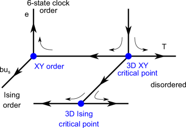
Where and are coefficients, is the amplitude of the strain and is the magnitude of the Néel vector. As shown in Fig. 5, for , in the absence of strain, this describes a six-state clock model, whose critical behavior is expected to be in the XY universality class. For , the Ising anisotropy dominates, and the critical behavior is in the Ising universality class oshikawaprb00 ; louprl07 . In general, the direction of the Néel vector will be determined by the competition between the strain and the crystalline anisotropy (See Supplementary Note 5.) This model explains why an Ising order is also induced in the 15 m thick bulk sample mounted by glue as the strain is quite small.
These conclusions also follow from a more microscopic model of spins on a honeycomb lattice with interactions that reflect the symmetries of the crystal. We consider an XY model with nearest-neighbor couplings that are modified by strain and have the form
| (2) |
distinguishing the coupling for spin polarizations “along” () and “perpendicular to” () the -th Mn-Mn bond and is a symmetry allowed cross coupling between orthogonal spin components and in each bond. The total energy is proportional to , where defines a misalignment angle of the spin orientation from the principal strain axis. As long as the response is linear, decreasing the amount of strain while keeping the same direction will not change the tipping angle. (See Supplementary Note 6 for more details.)
The direct imaging of Néel vector switching in the monolayer goes beyond previous works of domain imaging in bulk AFM samples fiebigreview05 ; fiebigjpd05 ; wadleynatnano2018 and opens the possibility of ultra-compact AFM spintronics. Our work also creates a new method to control the 2D antiferromagntism besides electric gating huangnatnano18 ; jiangnatmat18 ; jiangnatnano18 and magnetic fields sunnat19 . Additionally, our imaging and strain-tuning methods are generically applicable to other van der Waals AFM materials including the intrinsic AFM topological insulator otrokovnature19 . Looking forward, we hope that the discovery of extremely strain-tunable AFM order in atomically thin MnPSe3 would stimulate further investigations in designing spatial strain patterns, to create spin pattern on demand for magnon propagation in low-dissipation terahertz spintronic devices. The monolayer MnPSe3 also provides a platform to study the Kosterlitz-Thouless transition in a truly 2D XY magnet with six-state clock order if the strain could be tuned to zero by a voltage-controlled piezo-stage mutchsciadc2019 . The atomically thin MnPSe3 might also be a good candidate for broadband, efficient upper-conversion as the gap is in the visible regime.
References
- (1) Costanzo, D., Jo, S., Berger, H. & Morpurgo, A. F. Gate-induced superconductivity in atomically thin MoS2 crystals. Nature Nanotechnology 11, 339–344 (2016).
- (2) Xi, X. et al. Strongly enhanced charge-density-wave order in monolayer NbSe2. Nature Nanotechnology 10, 765–769 (2015).
- (3) Wu, S. et al. Observation of the quantum spin Hall effect up to 100 kelvin in a monolayer crystal. Science 359, 76–79 (2018).
- (4) Huang, B. et al. Layer-dependent ferromagnetism in a van der Waals crystal down to the monolayer limit. Nature 546, 270–273 (2017).
- (5) Mak, K. F., Shan, J. & Ralph, D. C. Probing and controlling magnetic states in 2D layered magnetic materials. Nature Reviews Physics 1, 646–661 (2019).
- (6) Němec, P., Fiebig, M., Kampfrath, T. & Kimel, A. V. Antiferromagnetic opto-spintronics. Nature Physics 14, 229–241 (2018).
- (7) Wadley, P. et al. Electrical switching of an antiferromagnet. Science 351, 587–590 (2016).
- (8) Saidl, V. et al. Optical determination of the Néel vector in a CuMnAs thin-film antiferromagnet. Nature Photonics 11, 91–96 (2017).
- (9) Cheong, S.-W., Fiebig, M., Wu, W., Chapon, L. & Kiryukhin, V. Seeing is believing: visualization of antiferromagnetic domains. npj Quantum Materials 5, 3 (2020).
- (10) Nair, N. L. et al. Electrical switching in a magnetically intercalated transition metal dichalcogenide. Nature Materials 19, 153–157 (2020).
- (11) Oshikawa, M. Ordered phase and scaling in Zn models and the three-state antiferromagnetic Potts model in three dimensions. Physical Review B 61, 3430 (2000).
- (12) Lou, J., Sandvik, A. W. & Balents, L. Emergence of U(1) Symmetry in the 3D XY Model with Zq Anisotropy. Physical Review Letters 99, 207203 (2007).
- (13) Cheong, S.-W. SOS: symmetry-operational similarity. npj Quantum Materials 4, 53 (2019).
- (14) Gong, C. et al. Discovery of intrinsic ferromagnetism in two-dimensional van der Waals crystals. Nature 546, 265–269 (2017).
- (15) Deng, Y. et al. Gate-tunable room-temperature ferromagnetism in two-dimensional Fe3GeTe2. Nature 563, 94–99 (2018).
- (16) Fei, Z. et al. Two-dimensional itinerant ferromagnetism in atomically thin Fe3GeTe2. Nature Materials 17, 778–782 (2018).
- (17) Thiel, L. et al. Probing magnetism in 2D materials at the nanoscale with single-spin microscopy. Science 364, 973–976 (2019).
- (18) Chen, W. et al. Direct observation of van der Waals stacking dependent interlayer magnetism. Science 366, 983–987 (2019).
- (19) Song, T. et al. Giant tunneling magnetoresistance in spin-filter van der Waals heterostructures. Science 360, 1214–1218 (2018).
- (20) Klein, D. R. et al. Probing magnetism in 2D van der Waals crystalline insulators via electron tunneling. Science 360, 1218–1222 (2018).
- (21) Wang, Z. et al. Very large tunneling magnetoresistance in layered magnetic semiconductor CrI3. Nature Communications 9, 2516 (2018).
- (22) Huang, B. et al. Electrical control of 2D magnetism in bilayer CrI3. Nature Nanotechnology 13, 544–548 (2018).
- (23) Jiang, S., Shan, J. & Mak, K. F. Electric-field switching of two-dimensional van der Waals magnets. Nature Materials 17, 406–410 (2018).
- (24) Jiang, S., Li, L., Wang, Z., Mak, K. F. & Shan, J. Controlling magnetism in 2D CrI3 by electrostatic doping. Nature Nanotechnology 13, 549–553 (2018).
- (25) Burch, K. S., Mandrus, D. & Park, J.-G. Magnetism in two-dimensional van der Waals materials. Nature 563, 47–52 (2018).
- (26) Gong, C. & Zhang, X. Two-dimensional magnetic crystals and emergent heterostructure devices. Science 363 (2019).
- (27) Gibertini, M., Koperski, M., Morpurgo, A. & Novoselov, K. Magnetic 2D materials and heterostructures. Nature Nanotechnology 14, 408–419 (2019).
- (28) Lee, J.-U. et al. Ising-type magnetic ordering in atomically thin FePS3. Nano Letters 16, 7433–7438 (2016).
- (29) Wang, X. et al. Raman spectroscopy of atomically thin two-dimensional magnetic iron phosphorus trisulfide (FePS3) crystals. 2D Materials 3, 031009 (2016).
- (30) Kim, K. et al. Antiferromagnetic ordering in van der Waals 2D magnetic material MnPS3 probed by Raman spectroscopy. 2D Materials 6, 041001 (2019).
- (31) Vaclavkova, D. et al. Magnetoelastic interaction in the two-dimensional magnetic material MnPS3 studied by first principles calculations and Raman experiments. 2D Materials (2020).
- (32) Huang, B. et al. Emergent phenomena and proximity effects in two-dimensional magnets and heterostructures. Nature Materials 1–14 (2020).
- (33) Long, G. et al. Persistence of Magnetism in Atomically Thin MnPS3 Crystals. Nano Letters 20, 2452–2459 (2020). PMID: 32142288.
- (34) Fiebig, M., Pavlov, V. V. & Pisarev, R. V. Second-harmonic generation as a tool for studying electronic and magnetic structures of crystals. JOSA B 22, 96–118 (2005).
- (35) Chu, H. et al. Linear magnetoelectric phase in ultrathin MnPS3 probed by optical second harmonic generation. Physical Review Letters 124, 027601 (2020).
- (36) Sun, Z. et al. Giant nonreciprocal second-harmonic generation from antiferromagnetic bilayer CrI3. Nature 572, 497–501 (2019).
- (37) Wiedenmann, A., Rossat-Mignod, J., Louisy, A., Brec, R. & Rouxel, J. Neutron diffraction study of the layered compounds MnPSe3 and FePSe3. Solid State Communications 40, 1067–1072 (1981).
- (38) Wildes, A., Roessli, B., Lebech, B. & Godfrey, K. Spin waves and the critical behaviour of the magnetization in MnPS3. Journal of Physics: Condensed Matter 10, 6417 (1998).
- (39) Wildes, A., Rule, K. C., Bewley, R., Enderle, M. & Hicks, T. J. The magnon dynamics and spin exchange parameters of FePS3. Journal of Physics: Condensed Matter 24, 416004 (2012).
- (40) Wildes, A. R. et al. Magnetic structure of the quasi-two-dimensional antiferromagnet NiPS3. Physical Review B 92, 224408 (2015).
- (41) Ressouche, E. et al. Magnetoelectric MnPS3 as a candidate for ferrotoroidicity. Physical Review B 82, 100408 (2010).
- (42) Lançon, D. et al. Magnetic structure and magnon dynamics of the quasi-two-dimensional antiferromagnet FePS3. Physical Review B 94, 214407 (2016).
- (43) Jeevanandam, P. & Vasudevan, S. Magnetism in MnPSe3: a layered 3d5 antiferromagnet with unusually large XY anisotropy. Journal of Physics: Condensed Matter 11, 3563 (1999).
- (44) Kim, K. et al. Suppression of magnetic ordering in XXZ-type antiferromagnetic monolayer NiPS3. Nature Communications 10, 345 (2019).
- (45) Kang, S. et al. Coherent many-body exciton in van der Waals antiferromagnet NiPS3. Nature 583, 785–789 (2020).
- (46) Wu, L. et al. Giant anisotropic nonlinear optical response in transition metal monopnictide Weyl semimetals. Nature Physics 13, 350–355 (2017).
- (47) Sa, D., Valenti, R. & Gros, C. A generalized Ginzburg-Landau approach to second harmonic generation. The European Physical Journal B-Condensed Matter and Complex Systems 14, 301–305 (2000).
- (48) Li, X., Cao, T., Niu, Q., Shi, J. & Feng, J. Coupling the valley degree of freedom to antiferromagnetic order. Proceedings of the National Academy of Sciences 110, 3738–3742 (2013).
- (49) Yin, X. et al. Edge nonlinear optics on a MoS2 atomic monolayer. Science 344, 488–490 (2014).
- (50) Casiraghi, C. et al. Rayleigh imaging of graphene and graphene layers. Nano Letters 7, 2711–2717 (2007).
- (51) Zhao, M. et al. Atomically phase-matched second-harmonic generation in a 2D crystal. Light: Science & Applications 5, e16131–e16131 (2016).
- (52) Liu, F. et al. Disassembling 2D van der Waals crystals into macroscopic monolayers and reassembling into artificial lattices. Science 367, 903–906 (2020).
- (53) Liu, Z. et al. Strain and structure heterogeneity in MoS2 atomic layers grown by chemical vapour deposition. Nature Communications 5, 5246 (2014).
- (54) Zhang, Q. et al. Strain relaxation of monolayer WS2 on plastic substrate. Advanced Functional Materials 26, 8707–8714 (2016).
- (55) Chen, X. et al. Electric field control of néel spin–orbit torque in an antiferromagnet. Nature Materials 18, 931–935 (2019).
- (56) Fiebig, M. Revival of the magnetoelectric effect. Journal of Physics D: Applied Physics 38, R123 (2005).
- (57) Wadley, P. et al. Current polarity-dependent manipulation of antiferromagnetic domains. Nature Nanotechnology 13, 362–365 (2018).
- (58) Otrokov, M. M. et al. Prediction and observation of an antiferromagnetic topological insulator. Nature 576, 416–422 (2019).
- (59) Mutch, J. et al. Evidence for a strain-tuned topological phase transition in ZrTe5. Science Advances 5, eaav9771 (2019).
I Methods
Sample Preparation
Single crystals of MnPSe3 were grown by the chemical vapor transport method. Elemental powders of high purity Mn, P, and Se were pressed into a pellet and sealed inside a quartz tube under vacuum. The tube was then annealed for a week at 730 ∘C to form polycrystalline MnPSe3 power, the composition of which was verified with powder X-ray diffraction. Crystals were then grown using the chemical vapor transport method with iodine as transport agent: 2 g of the powder and 0.4 g of iodine crystals were placed at the end of a quartz tube, which was sealed off at 13 cm length under vacuum. The sealed tube was then set in a temperature gradient of 650/525 ∘C for four days to transport the starting materials placed at the hot end to the cold end. The Mn : P : Se ratio was measured to be 1.00(1) : 0.96(1) : 3.07(1) with energy-dispersive X-ray spectroscopy. The ultra-thin samples were prepared by a standard mechanical exfoliation process on Si substrates with 90 nm thick SiO2 from a few MnPSe3 bulk crystals with 68 K. The samples were put into a vacuum environment after exfoliation. The total exposure time in air for samples exfoliated in a glove box is less than one minute before loading into the cryostat where the sample is under vacuum.
SHG microscopy
The sample was loaded on a metal platform in a closed-cycle cryostat, and the temperature of the metal platform was controlled by a local heater, which induces only a sub-micron shift of the sample position between 5 K and 100 K. An ultrafast 800-nm Ti-sapphire laser pulse with a duration 50 fs at the repetition rate of 80 MHz was focused onto a 2 m beam spot on the sample under normal incidence. A typical laser power of 200 W was used except for the following cases. 500 W was used for thick flakes and bulk crystals. In the bilayer sample in Extended Data Figure 6, 400 W was used. No sample damage was observed during the measurement. The reflected SHG light was collected by an 50 objective and reflected by a dichroic mirror or a D mirror into a photomultiplier tube connected with a lock-in amplifier or a photon counter. The photon counter was locked to the 80 MHz in order to reduce the dark count below 0.2 counts per second (cps) without cooling the photomultiplier by cryogen. The detection sensitivity in the experiments was 0.2 counts per second. Because the parallel signal is one order smaller than the crossed signal, the polarization extinction ratio was important when measuring parallel patterns. The polarization of the fundamental light was controlled by a half-wave plate as well as a linear polarizer. The polarization of second-harmonic light was analyzed by a linear polarizer. The SHG imaging microscopy was achieved by moving the sample with three Attocube nano-positioners.
Strain Tuning
We exfoliated MnPSe3 on PDMS with a square shape and applied tensile strain on two sides of the PDMS by a micro-manipulator. The stretched PDMS was then attached to a gold-coated sample platform. The strain was estimated by measuring the length change along the stretching direction in the optical image. A low transfer ratio () from PDMS to the sample was observed. To change the sample’s strain direction, we peeled off the PDMS from the sample platform and then stretched it in another direction. To apply strain along the 45∘ and 135∘, we cut the four corners of the PDMS to form a smaller square shape in order to reduce twisting while applying strain. The error bar of estimation of strain strength is and the error bar of the strain direction is .
Symmetry analysis for SHG polar patterns
For the SHG patterns above , the angle dependence are described by
| (3) |
| (4) |
is the angle of the incident linear polarization with respect to the axis of the crystal. Note that in the fit there is also a constant angle shift in , which is the angle between the horizontal axis in the lab and the crystal axis. For the SHG patterns below , we fit the crossed polar patten by
| (5) |
and denote the node direction in the polar pattern as the Néel vector direction. is the angle of the direction of the Néel vector with respect to the crystal axis. See Supplementary Note 1 for more details.
II Acknowledgement
We thank S.W. Cheong and O. Tchernyshyov for helpful discussions. This project is mainly supported by L.W.’s startup package at the University of Pennsylvania. The development of the SHG photon counter was supported by the ARO YIP award under the Grant W911NF1910342 (L.W.). The measurement by the atomic force microscopy was supported by the ARO MURI award under the Grant W911NF2020166 (L.W.). The acquisition of the oscillator laser for the SHG experiment was supported by NSF through Penn MRSEC (DMR-1720530). E.J.M. acknowledges support from NSF EAGER 1838456. C.L.K was supported by a Simons Investigator grant from the Simons Foundation. D.G.M acknowledges support from the Gordon and Betty Moore Foundation’s EPiQS Initiative, Grant GBMF9069. H.W. and X.Q. acknowledge support from NSF DMR-1753054 and Texas A&M University President’s Excellence Fund X-Grants Program. B.X and C.B. are supported by the Schweizerische Nationalfonds (SNF) by Grant No. 200020-172611. The DFT calculations were conducted with the advanced computing resources provided by Texas A&M High Performance Research Computing.
III Author Contribution
L.W. conceived the project and coordinated the experiments and theory. L.W. designed the SHG imaging setup and built it with Z.N.. Z.N. performed the experiments and analyzed the data under the supervision of L.W.. L.W., Z.N., E.M., and C.K. discussed and interpreted the data. E.M. performed the spin model calculation. C.K. performed the Landau theory calculation. A.H. and D.M. grew the crystals and performed magnetization measurements. H.W. and X.Q. performed first-principle calculation. B.X. and C.B. performed the optical conductivity measurement. L.W. and Z.N. wrote the manuscript from input of all authors. All authors edited the manuscript.
IV Addendum
Data availability: All data needed to evaluate the conclusions in the paper are present in the paper and the Supplementary Information. Additional data related to this paper could be requested from the authors.
Competing Interests: The authors declare that they have no competing financial interests.
Correspondence: Correspondence and requests for materials should be addressed to L.W. (liangwu@sas.upenn.edu)
Supplementary Information for “Imaging the Néel vector switching in the monolayer antiferromagnet MnPSe3 with strain-controlled Ising order”
Supplementary Note 1. Symmetry analysis of SHG responses
Above the Néel temperature , the bulk MnPSe3 has rhombohedral (ABC) stacking and belongs to the point group () and the space group 148, where all of the mirror symmetries are broken, but the threefold rotation symmetry along the axis and the inversion symmetry are present wiedenmannssc81 . Below , the material forms Néel AFM order, which breaks the inversion symmetry and the threefold rotation symmetry and allows all of the 18 non-zero terms in .
Here we consider two sources contributing to the SHG signal: an electric-quadrupole (EQ) contribution from the lattice and an electric dipole (ED) contribution related with Néel vector (), . generally depends on the Néel vector (). The EQ contribution is present at all temperature while the ED one is only allowed below .
1.1 Electric-quadrupole contribution
First, we consider EQ contribution . For a normally incident beam on the plane, we have and . The point group symmetry allows eight non-zero elements with two independent values, and . Assuming the polarization of incident light is at an angle of with with respect to the axis, we have . For parallel and crossed patterns, the detected polarization is along and , respectively. Therefore, the SHG intensity above Néel temperature is
| (S1) |
| (S2) |
Both of them are sixfold rotationally symmetric with the same amplitude, and peak positions are dependent on the ratio of and . A fit to SHG data at 100 K in a 100-nm thick MnPSe3 sample is shown in Fig. 1b in the main text. Note that in the fit there is a shift of the angle by a constant set by the angle between the lab axis and the crystal axis.
1.2 Electric-dipole contribution from the Néel AFM order
Next, we consider the ED contribution related with the Néel vector . One could also write this term to relate with the Néel vector by , where . Since all the non-zero are allowed in the AFM ordered state, it is impractical to fit the polar patterns to extract the components. Under normal incidence, there are still six non-zero independent terms in the ordered phase.
Consider that the crossed polar patterns from monolayer to bulk are quite similar at all temperature below the transition temperature, to derive a simpler relationship with the Néel vector, we use a Talyor expansion at (near the phase transition) to expand up to the linear term,
| (S3) |
Then one can define a 4th-rank tensor and the ED term is written as . Note that the Néel vector behaves the same as an electric field under the threefold rotation operation, the inversion operation, and the reflection operation vertical to the axis in the lattice of MnPSe3. The former two are the symmetry operations in the lattice of a multi-layer MnPSe3 while the last one is an additional symmetry operation in the lattice of the monolayer MnPSe3 with the spins along the axis. Therefore, we could treat the Néel vector similar to an electric field in the symmetry analysis. The tensor has the lattice symmetry in paramagnetic phase. The non-zero components of the ED SHG susceptibility tensor in the ordered state could be derived from the symmetries of the susceptibility tensor in the high-temperature phase and the order parameter savalenti00 , , where is a component of the Néel vector. Note that the symmetry of is higher than the general that applies to the temperature below because we only consider up to the linear order in Equa. S3. Therefore, applies to the temperature near the phase transition and could be extended to the general ED SHG susceptibility tensor by considering higher-order terms. Note that the discussion in this paragraph applies to monolayer and bulk samples.
Monolayer MnPSe3 has a mirror symmetry along plane and a threefold rotation symmetry along axis without the AFM order. With the lattice symmetry and the exchange symmetry of indices and , one can write the tensor to be
| (S4) |
To calculate polarization dependent SHG signal, we define to be the angle of incident light polarization and to be the angle of the Néel vector with respect to the axis. Therefore and . Eventually one gets
| (S5) |
| (S6) |
These results enable us to identify the direction of Néel vector. It is interesting to note that only the orientation but not the shape and magnitude of ED-SHG patterns would change when the direction of Néel vector changes.
Layer stacking in multi-layer MnPSe3 breaks the mirror symmetry while maintain the threefold rotation symmetry in lattice. Therefore more tensor elements need to be considered. The new tensor is
| (S7) |
Considering a incident electric field and Néel vector , the output second-order response is then
| (S8) |
| (S9) |
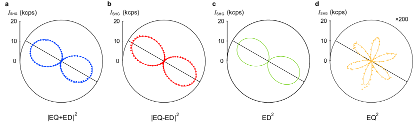
When the crossed pattern has a node (that crosses zero), according to our simulation, there are two possibilities: (1 ) is much smaller than ; (2) and are almost in phase. In the first case, the node direction in the across pattern is the Néel vector direction. In the second case, their direction are off by an angle of . To summarize, the crossed polar pattern could be described by , where is a constant.
1.3 Coupling between ED and EQ terms
In our experiment, the in-plane uniaxial anisotropy caused by the strain pins the Néel vector to an Ising type. Therefore, the in-plane Néel vector can only switch between two opposite directions reversed by the time-reversal operation. If the SHG signal is purely from the ED contribution, there is no way to distinguish these two domains because of the lack of phase information in the SHG measurement. However, by interfering the ED contribution with the EQ contribution, it is possible to get different responses from two domains even though the EQ term is much smaller than the ED term. The total SHG intensity is
| (S10) |
| (S11) |
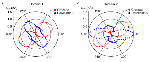
In the main text, we show the exsistence of two different crossed patterns corresponding to two Ising domains. To test whether the data are consistent with the above analysis, we fit two crossed patterns of two Ising domains from a 15 m sample using Equa. (S11). Crossed polar patterns for domain 1 and 2 are plotted by blue and red dots in Supplementary Figure 1. Since the EQ term is not expected to change with temperature, we use the EQ term in the crossed pattern above Néel temperature. The crossed pattern measured at 100 K is shown by yellow dots in Supplementary Figure 1d. Note the 100 K pattern is magnified by 200 times. We fit the three curves simultaneously with the fitting weight of the 100 K data being 200 times larger than the other two at 5 K. The best fit results are shown in solid lines in Supplementary Figure 1. It matches well with all of the three patterns. The green and yellow solid lines represent the extracted pure ED and EQ contributions. In thick samples, the magnitude of the crossed pattern signal remains almost the same but with a small angle change in the node direction when domain change happens because of the much larger ED contribution than the EQ one. In thin samples, especially in the monolayer (see main text Fig. 3j), crossed patterns of two domains look more different in terms of the orientation, which results from a smaller ratio between ED term and EQ term.
The ED term in the parallel configuration at 5 K is around 4–6 times larger than the EQ term above (for example, see Supplementary Figure 4 on a 50 nm sample.). It induces a significant change of the polar pattern when the Néel vector reverses. We have showed the switching of parallel polar patterns of a 15 m thick, monolayer and bilayer samples. Here we show the domain switching in a 100 nm thick sample and the polar patterns corresponding to two domains are shown in Supplementary Figure 2. Note that this is a 3rd 100 nm sample which is different from those in Fig. 1b and Fig. 2d-f in the main text.
1.4 SHG patterns in the existence of out-of-plane Néel vector component
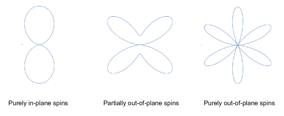
As discussed in the main text, the neutron scattering experiment reveals that spins in MnPSe3 are in-plane wiedenmannssc81 . From SHG patterns, one can also tell whether the spin direction is out-of-plane or in-plane. From Equa. S3 and Equa. S7, one can obtain a sixfold SHG patterns when has a pure z-component and twofold SHG patterns when has no z-component. When the has both in-plane and out-of-plane components, the SHG pattern is neither twofold nor sixfold patterns. Examples of crossed patterns in each case are shown in Supplementary Figure 3. Based on this analysis, the twofold crossed patterns we observe in the experiment also support the picture of in-plane Néel vector.
1.5 Temperature dependence of SHG patterns in a 50 nm thick flake exfoliated on SiO2/Si
Here we examine the validity of neglecting the higher-order terms in the Taylor expansion of second-order susceptibility. When the temperature is close enough to the Néel temperature, the Néel vector is small, and therefore, it is reasonable to neglect higher-order terms of . However, when the sample temperature is far below the Néel temperature, all of the 6 non-zero terms in second-order susceptibility are necessary. To test this, we measure the temperature dependence of SHG patterns at one spot of a 50 nm thick flake. In Supplementary Figure 4a,b, we show the data for crossed and parallel patterns in domain 1 and in Supplementary Figure 4c, we show the parallel pattern for domain 2. Using Equa.S10 and S11 we perform a simulation of the experiment data with (shown in Supplementary Figure 4d-f). The experiment and simulation match well across the whole temperature in crossed patterns. In parallel patterns, however, the simulation using Equa. S10 matches the experiment near Néel temperature: in both domains 1 and 2, the experimental data is reproduced by the simulation above 60 K, but not captured well below 50 K. We also test a 4th 100-nm sample and reached the sample conclusion that Equa. S10 works above 60 K. The break-down in parallel pattern indicates other terms should be considered at low temperature, while for the crossed pattern, Equa. S11 is good enough to capture the key factors such as the amplitude and the node direction.
Supplementary Note 2. DFT calculation of the polar pattern from ED contribution
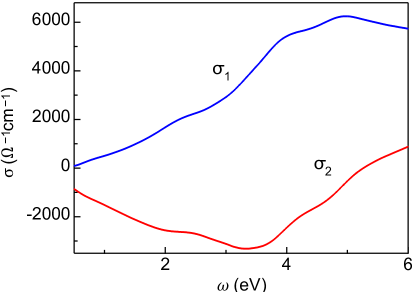
To see how the polar pattern looks like by considering all of the non-zero terms, we performed density functional theory calculation. Electronic structure of antiferromagnetically ordered monolayer MnPSe3 with spin polarization aligned along direction ( axis) shown in Supplementary Figure 5a. was calculated using first-principles density-functional theory (DFT) implemented in the Vienna ab-initio Simulation Package with a plane-wave basis and the projector-augmented wave method. We adopted the Perdew-Burke-Ernzerhof (PBE)’s form of exchange-correlation functional within the generalized-gradient approximation (GGA) and a Monkhorst-Pack k-point sampling for the Brillouin zone (BZ) integration. An energy cutoff of 300 eV for the plane-wave basis and a Monkhorst-Pack k-point sampling of 24 24 1 were applied. Spin-orbit coupling was taken into account at the full-relativistic level. Hubbard correction was included in the DFT-PBE calculations with 3.9 eV to account for the correlation effect from transition metal. The monolayer structure was extracted from the experimental bulk structure wiedenmannssc81 which holds in-plane antiferromagnetically-ordered monolayer MnPSe3 with spin polarization aligned along direction (AFM-x, see Supplementary Figure 5a). The electronic band structure and spin density along x were shown in Supplementary Figure 5b. The calculated band-gap is 1.6 eV, which was smaller than the experiment value 2.32 eV measured on a bulk sample grassoJOSAB99 as expected for PBE+U. Our room temperature optical conductivity measurement shown in Figure 11 is qualitatively the same as the previous work grassoJOSAB99 . Moreover, the spin density is localized around Mn atoms with spin polarization along axis. Note that the calculation does not take the exciton effect into consideration.
The magnetic point group of multi-layer (with the Néel vector along axis) is ; hence the parity-time-symmetry allows c-type SHG with all components being symmetry allowed. SHG susceptibility tensor was calculated by using an in-house developed first-principles nonlinear optics package (iNLO)huananolett2017 ; huasciadv2019 interfaced with VASP. Total 100 electronic bands were included in the calculations, and a small imaginary smearing factor of 0.05 eV was included in the fundamental frequency in the denominator of susceptibility tensor. The result at the incident photon energy of 0.83 eV is shown in Supplementary Figure 5c, considering that the gap size in the calculation is smaller by 0.73 eV and the incident photon energy in the experiment is centered at 1.55 eV. The anisotropy plot indicates that the lobes in the crossed pattern are mainly pointing perpendicular to the direction of the Néel vector. In other words, the node direction in the crossed pattern is close to the Néel vector direction, which supports the above analysis in Supplemantary Note 1. We also point out that we looked at the node direction over a wide energy range from 0.6 eV to 1.2 eV for the incident photon energy in the calculation. It is always within 30∘ from the Néel vector. An example of the polar patterns at 1.1 eV is shown in Supplementary Figure 5d, which also looks quite similar to the experiment.
Supplementary Note 3. More SHG data
3.1 More SHG imaging about AFM domains on a bulk crystal
Here we show SHG mapping about AFM domains on a 30 m bulk crystal in Supplementary Figure 6. The incident and detecting light polarization are shown on the top of each figure. Supplementary Figure 6a. is measured when the peak of the crossed pattern is reached. The darker lines indicated by the white arrows are scratches on the sample surface, while other darker lines indicate the AFM domain walls between 180∘ domains. Supplementary Figure 6b,c. show SHG intensity mapping in the parallel channel with two different polarizer angles. Two different domains are clearly distinguishable by different SHG intensity in both mappings with sharp contrasts. The outlines of the domains in the three figures match well. These observations are consistent with our previous discussion on the domain wall between two Ising domains.
3.2 SHG polar patterns and mapping on atomically thin few-layer MnPSe3
Supplementary Figure 7 shows an SHG intensity mapping in a multi-layer sample with different domains. The measuring polarization is chosen to be near the peak of areas marked by the red arrow. Regions with homogeneous thickness and same AFM domains are outlined by white lines (and gray line for the 4-layer sample) . The arrows indicate the node direction in the crossed patterns. In each region, the crossed polar pattern is measured and shown beside the intensity mapping. Note that part of the 2L sample with the tail shape on the bottom left corner has a different Néel vector direction probably due to a different strain direction. Nevertheless, as we mentioned in the main text, all of the samples measured in this work, including these few-layer ones, all show two-state (Ising) ground state with in-plane spins across thermal cycles at randomly selected positions we measure.
3.3 Critical behavior fitting
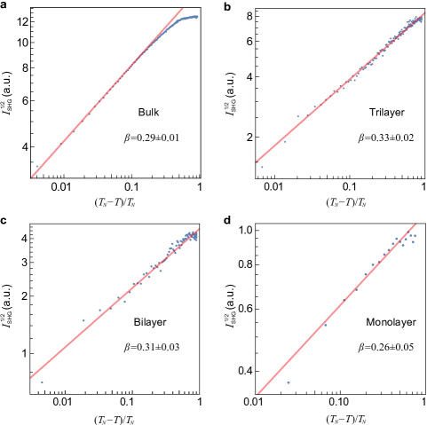
The order parameter follows with being the critical exponent in a continuous phase transition. Since is proportional to the order parameter savalenti00 , on can get where is a constant coming from the EQ contribution. In Supplementary Figure 8, we plot that was shown in Extended Data Figure 5 as a function as in a log-log plot. The slope of the linear curve near the origin is the critical exponent . The experiment data and the best fit of bulk (a), trilayer (b), bilayer (c) and monolayer (d) samples are showed. Note the fitting error is pretty high in monolayer due to the uncertainty of the Néel temperature. Overall, the critical exponent is 0.3, and the critical exponential of 0.29 ( 0.01) is in the 15 m thick bulk crystal is most reliable considering the very dense temperature step in the measurement and the highest signal-to-noise ratio. From the critical component itself, even though it is close to the 3D Ising model () than the 3D XY model (), it is not very obvious that the phase transition belongs to the Ising universality class since the difference in is small. Nevertheless, the collapse of the temperature-dependent SHG on two curves is a strong evidence for the Ising order.
3.4 Néel vector distribution in multi-layer MnPSe3
Since the crossed pattern nodes are locked to the Néel vectors, it is possible to map the spatial distribution of Néel vector within a MnPSe3 flake. To perform Néel vector mapping on thick flakes of MnPSe3, a flat area of a 80 m 80 m on a 100-nm MnPSe3 flake is chosen as indicated by the black square in Supplementary Figure 9a. Contrary to the uniform image under an optical microscope (Supplementary Figure 9a), the SHG signal, however, is highly inhomogeneous in this area (Supplementary Figure 9b). First, we measure the crossed patterns in the selected points marked with white circles in Supplementary Figure 9b. Both the magnitude and the orientation of Néel vectors are non-uniform revealed by crossed patterns shown in Supplementary Figure 9c. To map the crossed patterns in the whole region, we measured the crossed polar patterns in each spot with a 2 m size and fit them by to get the direction of the Néel vectors first. The lines in 9d represent the spatial distribution of the extracted directions of the Néel vectors. The directions of the node in crossed patterns are shown by the orientation of the line as well as the color of the line segments. Supplementary Figure 9e shows the histogram of the orientations of Néel vectors.
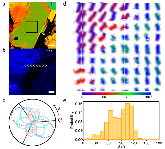
According to our previous analysis, the magnitude of the crossed pattern should not change if the direction of Néel vector changes in an unstrained thick flake. However, the from the fit shows the magnitude of crossed patterns is usually not the same at different positions. The magnitude of the Néel vector is represented by the length of the line segments. To resolve this inconsistency, we hypothesize that the orientation of the Néel vector could be different in different layers, probably due to the weak interlayer coupling.
We consider a multi-layer sample consisting of a few layers in a domain where the node direction of the crossed pattern points to and another few layers with the node direction pointed along . For simplify we assume each layer produces same second-harmonic electric field. Then we can derive the total SHG signal in crossed pattern detected with incident polarization to be
| (S12) | ||||
| (S13) |
where and and are constants determined by A and B. By tuning A and B, we can observe a crossed pattern with an arbitrary direction and amplitude for the Néel vector. Therefore, the experiment results in unstrained thick MnPSe3 could be explained by contributions between different Néel vectors in different layers.
3.5 Aging effect of a bilayer MnPSe3 sample in air
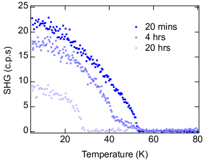
We tested the degradation of a bilayer MnPSe3 by exposing it to air. We exposed the same sample in air for 20 mins, 4 hours, and 20 hours and measured the SHG intensity and the transition temperature. During each exposure, the sample was stored in an atmospheric environment with relative humidity less than 30%. With the increase of exposure time, the SHG intensity and the Néel temperature decrease (Supplementary Figure 10). We conclude that the MnPSe3 is air-sensitive in its ultra-thin forms.
Supplementary Note 4. Strain dependent Néel vector distribution
First, we discuss how we determine the strain strength in MnPSe3 flake and PDMS substrates. We show optical images of the strained sample presented in Fig. 4 in the main text. Images on the sample as-exfoliated and under uniaxial strain in four different directions are shown in Supplementary Figure 12. In each direction, a strain is added to the PDMS substrate by a micro-manipulator. Supplementary Figure 12a and b show the distance change between two bulk flakes (marked by the solid lines) before and after applying the strain, where elongation of 15-16% is observed in the strained substrate. We also made an estimation that around 2% strain is added to the sample by comparing the change of the length of the sample before and after adding the strain (shown in Supplementary Figure 12c-e). Note that the error bar is around 0.5 , and the strain strength on different sample positions is possible to be slightly different because of the finite sample size liunatcomm14 . In Supplementary Figure 12d-g, optical images of the sample with different strain directions are shown. Nevertheless, as Fig. 4 in the main text shows that the SHG polar patterns are rotated and that the SHG intensity is uniform, strain is obviously added to the sample to align the Néel vectors. We hope that future Raman scattering experiments could determine the strain direction and strength more accurately. In our experimental, we could control strain direction within 10 degree, and the direction is more important. As shown in the microscopic spin model, small strain locks the Néel vector direction, and increasing the strain strength does not further tip the Néel vector in the linear response regime. Our SHG polar pattern measurement shows that the Néel vector is aligned towards the strain direction, and therefore, the conclusion of strain-controlled Ising order is valid even though the method of determining the strain strength by optical images (with cracks in the samples sometimes) might be less accurate than Raman scattering.
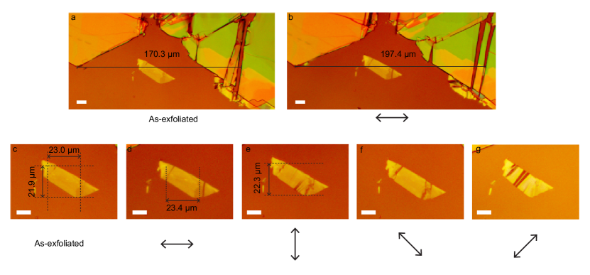
We investigate the effect of the strain on the Néel vector by applying different strength of strain along one direction on a MnPSe3 flake with a thickness of 10 nm determined by atomic force microscopy measurement. The data are shown in Supplementary Figure 13. 7.5% and 15% strain are added to the PMDS substrate and the strain on the sample is estimated by the strain on the PMDS and a transfer ratio of 13%. When the sample is as-exfoliated and under 1% and 2% elongation, we map the node direction in the crossed patterns using the same method as described in Equa. S11. When the sample is as-exfoliated, the node directions do not point to a specific direction. When 1% strain is applied, the node direction in most regions points to the direction of the stretched direction except the region on the right edge. When we further add strain to 2%, the node direction points to the stretched direction across the whole sample. Note that because of the small sample size, the strain direction near the edge might be more influenced by the sample shape or the substrate during exfoliation process instead of the externally applied strain, which may explain the observation that it is harder to align the Néel vectors on the edges.
The PDMS substrate is not a good thermal conductor when it is 30 m thick, and it can induce a 10 K temperature difference between the sample and the platform, which is calibrated by measuring the transition temperature of a thick ( 50 nm) flake sample on the same PDMS substrate. We then measure the with calibrated temperature as shown in Supplementary Figure 13j-i. There is no observable change (within 1 K) between these three cases.
Supplementary Note 5. Landau theory
Here we consider a Landau theory for the staggered magnetization . Symmetries constrain the terms that can appear in the expansion. We have the rotationally invariant tensor , which allows , and planar symmetry allows . We assume that this term is large, so that . For in the plane, the 3-fold rotation symmetry, along with time reversal allows a term . This identifies an allowed rank 6 tensor that can be contracted with .
Strain is described by a symmetric second rank tensor , whose principal axes describe the directions of compressive and tensile strain. To lowest order in the strain, a term is allowed.
It is easiest to describe the magnetization in polar coordinates, . Then, the crystalline anisotropy gives . The symmetric strain can be diagonalized with a rotation about the axis by an angle . This term then gives .
The Landau expansion (to lowest order in the coupling to strain) then takes the form
| (S14) |
where . Here is the mean field critical temperature for . , where is the magnitude of the Néel vector.
Minimizing with respect to and is equivalent to doing mean field theory. For , this gives
| (S15) |
with the mean field exponent .
For the critical behavior fluctuations are important and mean field theory breaks down. To get a better description of this, we can integrate out massive fluctuations in the magnitude to obtain an effective theory for , which has the form,
| (S16) |
As shown in main text Fig. 5, for this reduces to the 6 state clock model. For it is in the Ising universality class, and the antiferromagnetic order parameter is locked to the strain axis with a constant tilt angle.
Supplementary Note 6. Spin model
Here we construct a more microscopic spin model to explain the spin-strain locking. Space group 148 is a chiral group with the point symmetry . The high temperature state has two Mn sites on a honeycomb lattice. Below the Nel temperature the two sublattice sites develop different spin polarizations. Thus the AF transition is a condensation of two fields giving the spin polarizations on the and sublattice sites. Notice that this does not lower the translational symmetry of the structure, but only assigns the spins to the two sublattice sites.
The starting model for the structure has easy plane anisotropy. So the minimal model has on site anisotropy
where and .
Strain is a time reversal even, traceless second rank tensor . Each link of the honeycomb lattice can be defined by an in-plane vector and in the presence of strain we deform the links according to
In the following we are going to treat just the traceless part of which allows for deformation but not dilation or compression. The change of the exchange constants in any bond should be but even under . We build the simplest model that does this. For any link define the unit vector and the projections
| , | ||||
| , |
To lock the spin direction to the strain we have to replace the isotropic coupling in the original model by
| (S17) |
distinguishing spin polarizations “along” and “perpendicular to” the -th link. If we keep the isotropic form of the nearest neighbor coupling it would exclude the possibility of any locking of the spin to the strain.
Combining the first two terms gives an expression like
so the first term just looks like the isotropic coupling and the spin-lattice locking comes from the second piece. To make this more transparent we notice that and , so in terms of the macroscopic spin fields and , it expresses as
where denotes the outer product, i.e. in component form . This contains an isotropic component that can be removed by explicitly writing this as an outer product
This means that one must distinguish between the “longitudinal” and “transverse” spin couplings in any link but that the lattice sum produces an effective isotropic exchange constant . The previous Landau expansion makes it clear that in the absence of strain the crystal field anisotropy can not appear at bilinear order in the spin Hamiltonian as indeed we find in this explicit model.
The above conclusion demonstrates that if the ’s (which are symmetry allowed and therefore always present) were actually the same in each link then the traceless term in parenthesis gives zero after the sum over bonds because it is an tensor averaged over a crystal with threefold rotational symmetry. Similarly, the lattice sum over the term gives zero since the prefactors have the symmetry of an tensor. However the trailing isotropic term gives a nonzero result after the lattice sum: and this contributes to the isotropic term of the spin Hamiltonian which then becomes
The situation for the cross terms is similar. We can write the symmetric cross term in the exchange in the form
Using the notation it is useful to write this
Explicitly, the quantity in brackets is
| (S22) |
Because of the tensor character of the coefficients a constant value of in each bond gives no contribution to the exchange coupling. In the absence of strain the lattice sum allows only the isotropic coupling.
Finally, the values of the exchange constants and (both scalars) can vary in each link depending on the strain, and presumably one can linearize them in the manner
where the subscript (1) denotes the coefficient of the linear term in the expansion in powers of the strain coupling. Then by combining all these expressions, we arrive at a result for longitudinal and transverse strain couplings we had previously
(Note that in this expression it is not necessary to explicitly remove the isotropic piece from the outer product because the summand includes only the traceless part of the strain tensor. In this case the lattice sum containing the factor does not affect isotropic spin coupling. If one were to restore the dilational strain the isotropic piece would then renormalize the effective isotropic in the model). Rewriting this in terms of the macroscopic spin fields
This last term has the requisite symmetries: it is even under and and is -even.
In the Nel state the moments on the two sublattices are collinear (antiparallel): , so one can rewrite this
| (S23) |
In this expression is the externally imposed (traceless) strain and the sum is over a triad of nearest neighbor bonds away from an sublattice site.
A similar analysis for the cross term allows for its variation as a function of strain, i.e. using the linearize piece we get
| (S24) |
Summing equations 2 and 3 over a triad of bonds from an site gives a matrix parameterized by and whose principal axes denote the best and worst orientations of the Nel field in the presence of a strain . Summing the second bracket from both equations gives a form
The terms proportional to try to align the Nel field along the strain axes, whereas the cross product terms tip the Nel with respect to .
This can be seen most simply by carrying out the sum in a chiral basis where . If the principle axis of the strain tensor is aligned at angle one finds that the lattice sum gives an anisotropic spin coupling expressed as a matrix
| (S30) | |||
where and defines a misalignment angle of the spin orientation . This shows that the role of the strain coupling is to source two units of angular momentum in the spin Hamiltonian and that if we ignore the cross-coupling term the Nel vector would have a favored alignment along a principal axis of the strain tensor. The cross-coupling term is symmetry allowed and it misaligns the Nel field. The amount of this misalignment, which determines the direction of the Nel phase just below the phase transition is measure of the relative strength of the cross term. This might explain the experimental impression that the misalignment is small. This would mean that the exchange is mostly determined by the separate longitudinal and transverse terms. Intuitively this makes sense since the presence of the mixed term is subtle effect having to do with the action of full crystal symmetries on the exchange. Note that this means that it does not appear if you were to analyze an isolated bond, but the largest exchange anisotropy can be expected from the geometry within each bond. That will tend to lock the Nel field to the strain direction.
So the conclusion is that a linear coupling to strain provides a director that can orient the Nel vector. Ignoring “cross coupling” of spin polarizations in each bond one would lock the favored Nel vector along a principal strain axis. Including it defines an intrinsic misorientation in the bilinear spin Hamiltonian. The previous Landau theory finds a competition between intrinsic sixfold lattice anisotropy and the direction determined by the strain. The lattice model says that the Nel field determined by the strain need not be exactly along a principal strain axis, but it would be in the absence of the cross coupling contributions to the exchange matrix.
References
- (1) Wiedenmann, A., Rossat-Mignod, J., Louisy, A., Brec, R. & Rouxel, J. Neutron diffraction study of the layered compounds MnPSe3 and FePSe3. Solid State Commun. 40, 1067–1072 (1981).
- (2) Sa, D., Valenti, R. & Gros, C. A generalized Ginzburg-Landau approach to second harmonic generation. Eur. Phys. J. B 14, 301–305 (2000).
- (3) Grasso, V. & Silipigni, L. Optical absorption and reflectivity study of the layered MnPSe3 seleniophosphate. J. Opt. Soc. Am. B 16, 132–136 (1999).
- (4) Wang, H. & Qian, X. Giant optical second harmonic generation in two-dimensional multiferroics. Nano Lett. 17, 5027–5034 (2017). PMID: 28671472.
- (5) Wang, H. & Qian, X. Ferroicity-driven nonlinear photocurrent switching in time-reversal invariant ferroic materials. Sci. Adv. 5 (2019).
- (6) Liu, Z. et al. Strain and structure heterogeneity in MoS2 atomic layers grown by chemical vapour deposition. Nat. Commun. 5, 5246 (2014).