A capacitive displacement system for studying the piezoelectric strain and its temperature variation
Abstract
A capacitive displacement system was constructed to measure the electric-field-induced piezoelectric strain in the simple form of either a bulk or thin film. The system can determine an AC displacement of 2 pm precisely by using a lock-in detection, and can measure the large displacement within a range of 25 m with a sub-nanometer resolution. The system can also be used to measure the variation in strain within a temperature range of 210 - 450 K, allowing the evaluation of the temperature coefficient of a piezoelectric constant and the studies on the effects of a phase transition on the piezoelectric response. Experimental results on quartz, PZT ceramics and thin films, and BaTiO3 confirm the capabilities of the developed system.
pacs:
77.65.-j, 77.84.Dy, 77.55.+f, 77.80.Bh, 07.10.Pz, 81.70.-qI Introduction
Piezoelectrics convert mechanical energy into electric energy or vise versa, and show direct or converse effects.Curie ; Jaffe ; Lines ; Uchino In a direct effect, electric charges are produced at the surface of the piezoelectric crystal in proportion to the applied force. Conversely, as a suitably oriented electric field is applied, the crystal changes shape (strains) in proportion to the electric field. Such properties provide piezoelectrics with a wide spectra of applications such as medical ultrasound imaging, ultra-precise positioning, and sonar sensing. With a combination of modern integration- and nano-technologies, piezoelectrics can also be used as nano-sensors, nano-actuators, or nano-transducers in modern smart devices.Muralt1995 ; Muralt1997 ; Damjanovic ; DeVoe Therefore, there has been increasing interest in developing novel applications of piezoelectric materials such as current piezoelectric energy harvesting, or interest in exploring green materials to replace Pb-containing piezoelectric materials.ZhangS1 ; McKinstry ; Liu ; Acosta ; FuAPL2007 ; FuPRL2008 ; FuAPL2008 ; Rodel ; FuJPC2011 ; FuAPL2011 ; FuJPC2013
Various techniques have been developed to study the piezoelectric properties.IEEE ; Berlincourt ; Bottom ; Pan ; Lefki ; Kholkin ; Kanno ; Christman ; Xu ; Durkan ; Kuffer ; FuJJAP ; Park The resonance technique is the most widely used methodIEEE with a measurement accuracy of approximately 2%.Fialka However, it has special requirements for the shape and dimensions of the sample for different vibrational modes, and thus it is difficult to be used for thin-film measurements owning to shape and dimension limitations. The Berlincourt meter or -meter Berlincourt based on a direct effect are also widely used to measure the value of the bulk, which also shows a high measurement accuracy of approximately 1%.Stewart With this method, an AC force and a pre-stress are applied to the sampleStewart , which may result in damage to a thin film. Thus, it is unsuitable for thin film measurements. Another commonly used technique is the interferometry method, which is based on the converse effect for determining the sample displacement driven by an AC field. The interferometry has a pm-resolution to precisely determine the small AC displacement and can be used for both bulk and thin films.Bottom ; Pan ; Kholkin However, the interferometry method is difficult to measure a large displacement in the micro-meter scale.
Herein, we demonstrate a capacitive displacement method that can be used to reliably and simply measure the electric-field-induced strain in the form of either a bulk or film. We also show that our system can detect an AC displacement of as small as 2 pm, which is comparable with the resolution of the interferometry method.Pan It can also measure a large displacement within a range of 25 m with a sub-nanometer resolution. Moreover, the developed system can be used to measure the variation of strain with temperature in a wide temperature range of 210 to 450 K, allowing an estimation of the temperature dependence of the strain or studies on the effects of the phase transition on the piezoelectric properties.
II System Design
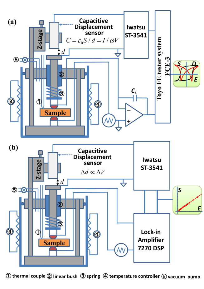
Figure 1 shows a block diagram of the system constructed for the strain measurement. The system can operate in two modes. Figure 1(a) shows the system running in normal mode, in which the displacement meter is combined with a commercial ferroelectric tester (Toyo FE tester system, FCE-3), allowing measurements of the strain and dielectric D-E hysteresis loops simultaneously for a bipolar electric field, as well as a large unipolar-field-driven displacement. Figure 1(b) show a schematic diagram of the lock-in amplifier mode, which can be used to precisely determine the strain piezoelectric coefficients at the zero field from the linear relationship between the AC displacement and voltage. It should be noted that the amplitude is used to express the values of all AC signals in this study.
As shown in Fig. 1, the displacement is measured by detecting the change in air capacitance that forms between the capacitive displacement sensor and object to be measured. Here, we have
| (1) |
where is the vacuum permittivity, is the sensor area, and is the distance between the sensor and object to be measured. When a voltage () with frequency is applied to the air capacitor, the applied voltage and the current flowing through the sensor have the following relationship
| (2) |
If is maintained at a constant value, then is proportional to the output voltage of the capacitive sensor. As shown in Fig. 1, is changed simultaneously as the sample is deformed by the applied electric field. We can therefore use this relationship to measure the sample deformation driven by the applied electric field by measuring the sensor output voltage. In our system, we use an Iwatsu ST-0403-50 capacitive sensor, which can probe the displacement within a range of 25 m with a resolution of 0.3 nm at 1 kHz, a linearity of 0.1%, and a frequency range from DC to 1 kHz. The capacitive sensor is equipped with an Iwatsu displacement meter ST-3541, which can provide a voltage output for data record (a voltage-displacement conversion coefficient of 2.5 nm/mV).
We found that sample mounting is of critical importance for reliably probing the sample displacement. Here, the sample is held between two cylindrical hemisphere electrodes with a diameter of 5 mm to provide a point contact between the sample and hemisphere electrodes. We also found that a linear bush is extremely effective in guiding the cylindrical shaft and providing a smooth and precise linear movement, allowing it to accurately measure the sample displacement. As shown in Fig. 1, a soft spring with a spring constant of 0.2 N/mm is used to make a reliable contact between the sample electrode and the hemisphere electrodes, and the compress force applied to the sample is estimated to be approximately 0.6 N, which is far lower than the commonly used value of approximately 10 N in a Berlincourt meter or a meter Stewart . This soft contact is extremely effective at preventing the damage to the sample, particularly for a thin film. A Z-stage is used to adjust the air capacitance distance for setting the zero output when the sample is not driven by an electric field. Essentially, if the sample can be held between the hemisphere electrodes, the measurement can be reliably performed. To confirm the reliable electrode contact directly by eye, the top electrode of the sample with a lateral size of larger than 1 mm is usually used for the measurements, whereas the bottom electrode is generally coated with a larger area for a convenient sample setup.
At present, the system can operate within a temperature range of 210 to 450 K. We use silicon oil as a heating medium to achieve a homogeneous sample temperature. In addition, silicon oil can also prevent a high voltage discharge, allowing the application of 10,000 V to a bulk sample. A silicon rubber heater of 100 W is used to heat the sample, whereas liquid N2 is used for cooling to low temperature. To prevent water condensation below the ice point, the sample chamber is evacuated using a vacuum pump. The silicon oil applied and the system can both undergo a thermal variation within a temperature range of 173 to 573 K. Thus, the measurement temperature can be expanded to a larger range.
III System Operation
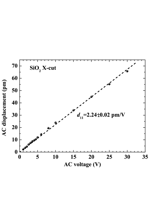
First, we used standard X-cut quartz to check the system operation in the lock-in amplifier mode. The X-cut quartz was driven by a small AC voltage, and the AC output of the displacement meter was fed into a lock-in amplifier (SIGNAL RECOVERY model 7265) to measure the AC displacement. As expected, a linear relationship was observed between the displacement and the applied voltage as shown in Fig. 2. Using a linear fitting, of the X-cut quartz was evaluated to be 2.24 0.02 pm/V, which is in extremely good agreement with the reported values (2.27 0.01 pm/VBottom , 2.32 pm/VPan , 2.22 pm/VGraham , 2.27 0.01 pm/VUchino2 , and 2.314 pm/VBhalla ). The results given in Fig. 2 also indicate that our system can accurately probe a 2-pm displacement that is comparable to a resolution of a double-beam laser interferometer Pan , and far better than the X-ray diffraction technique.Bhalla Because the SIGNAL RECOVERY (model 7265) lock-in amplifier applied can provide a full-scale sensitivity of 2 nV, which corresponds to a displacement resolution of 5 fm, it is possible to improve the measurement resolution of our system.
We then used commercial Pb(Zr1-xTix)TiO3(PZT) ceramics with a diameter of 10 mm and a thickness of 1 mm to examine the system operation in normal mode (without a lock-in amplifier) for measuring the large sample displacement. Figure 3 shows the simultaneously recorded dielectric and displacement loops under the application of a bipolar field. From the butterfly displacement loop, we can see that this PZT sample shows a deformation of several micro-meters during polarization switch driven by the bipolar field. When a unipolar voltage of 5,000 V is applied to the samples, it shows a displacement of approximately 2 m, as shown in Fig. 3 (c). Both the non-linearity and hysteresis of the displacement are reduced by reducing the unipolar voltage. From Fig. 3(d), a 45-nm displacement can be read at a voltage of 100 V. At this small voltage, the ratio between displacement and voltage is calculated as 450 pm/V, which is extremely close to the value of 441 pm/V obtained using ZJ-6B Quasi-Static Piezo /-meter made by the Institute of Acoustics, Chinese Academy of Sciences, which has a measurement accuracy of . Thus, we can use the ratio between strain () and electric field () at a low field (for example = 1-2 kV/cm) to estimate the piezoelectric coefficient of the sample.
IV Thin film measurements
After examining the system reliability when using standard quartz and PZT ceramics, we then use it to study the displacement of a PZT thin film. The film used has a composition of and a thickness of 1 m, and was prepared through a chemical solution deposition technique on a silicon substrate with a Pt bottom electrode. A top Au electrode with a diameter of 1 mm was then coated for the measurements. For easier measurements, the back side of silicon substrate without a PZT film was also coated by Au and connected to the Pt bottom electrode.
Figure 4(a) shows the dielectric and displacement hysteresis loops of the PZT film. In a normal mode operation without a lock-in amplifier, it is difficult to measure a nanometer-order displacement with a high resolution. To improve the resolution, we conducted 200 measurements and took the average, allowing us to obtain a displacement hysteresis loop of a PZT film with an extremely good resolution, as shown in Fig. 4(a). This film shows a displacement of approximately 2.4 nm as driven by a unipolar voltage of 20 V (corresponding to an electric field of = 200 kV/cm), as shown in Fig. 4(b). The large noise in the unipolar measurement is due to the smaller number of average measurements (20). We then used this unipolar measurement result to estimate the high field piezoelectric effect of the PZT film, which shows an effective piezoelectric coefficient of 120 pm/V at = 200 kV/cm. In addition, it seems that one can directly apply a large field to drive the film deformation for application without a poling process.
We then measured the strain piezoelectric coefficient at a zero-field after the PZT film was poled by unipolar field measurements. An AC electric field lower than the coercive fields was applied to the film to measure the AC displacement using a lock-in amplifier mode. It should be noted that if the applied AC field is larger than , the polarization state of the poled PZT film will be destroyed owing to the polarization switching. As expected from the piezoelectric effects, a linear relationship was observed between the displacement and applied voltage in Fig. 4(c). A linear fitting gives a value of pm/V for this PZT film. This value is half the value evaluated from the unipolar measurements at = 200 kv/cm. This difference can be explained by the difference of the poled regions in the film between these two different measurement techniques. The AC lock-in technique detects the piezoelectric response at the zero field of the remanent polarization after poling. By contract, the unipolar field measurement probes the piezoelectric response at an extremely high field of 200 kV/cm, which will result in larger poled regions in the film, and thus a larger polarization than the remanent polarization after poling. This is also evident from the D-E loop shown in Fig. 4(a). In addition, the lower value of this PZT film as compared with the ceramics samples is affected by many factors such as the film quality, orientation, and polarization relaxation. When comparing the dielectric loop of the ceramics (Fig. 2(a)) and that of the film (Fig. 4(a)), we can see that the remanent polarization of the film ( = +8 C/cm2, = -12 C/cm2) is much lower than that of PZT ceramics ( of 40 C/cm2). In addition, the polarization in a thin film is unstable after removing the applied field. However, the value obtained here falls within the reported range of the PZT films.Setter ; Taylor ; Gerbe The above results clearly indicate that the developed system is capable of probing the piezoelectric effects in a thin film.
V Temperature variation measurements
Some piezoelectric applications may involve environments where the temperature is different from room temperature. It is therefore necessary to characterize the behavior of the piezoelectrics over a range of possible operating temperatures. There are some reports on the temperature dependence of the piezoelectric properties including the piezoelectric coefficients, the elastic compliance coefficients, and the electromechanical coupling factors, which are commonly measured using a resonance method. Zhang ; Yokosuka ; ZhangS ; Sabat However, there is a lack of understanding of the temperature variation of the electric-field induced strain in a piezoelectric, which is of critical importance for actuator applications. We thus developed our system to be capable of measuring the piezoelectric strain within a temperature range of 210 - 450 K, which is important for practical applications.
Here, we use the PZT ceramics shown in the above measurements and BaTiO3(BTO) ceramics to demonstrate the temperature operation of our system. The measurement is conducted during the cooling process at a cooling rate of 1 K/min. For each temperature measurement, we first measure the dielectric and displacement loops under the application of a bipolar field. We then apply unipolar fields with maximum bipolar field (50 kV/cm for PZT and 30 kV/cm for BTO), 10 kV/cm, and 2 kV/cm, respectively, to measure the displacement dependence on the field.
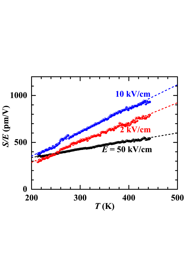
Figure 5 shows the temperature dependence of dielectric and strain hysteresis loops under the application of a bipolar field, and the unipolar field driven strain of PZT ceramics. The used PZT ceramics has a Curie point of 570 K (cooling) determined from the dielectric measurement. It can been seen that the polarization increases by reducing the temperature. By contrast, the strain response decreases upon cooling. Figures 5 (c) and (d) show the temperature variation of the strain at a unipolar field of 50 kV/cm, 10 kV/cm, and 2 kV/cm. Here, we use the ratio of the maximum strain () to the maximum unipolar field () to evaluate the piezoelectric strain response at different electric fields. The value can be considered an effective piezoelectric coefficient in different fields. In particular, the value at = 2 kV/cm is extremely close to the value obtained by a -meter.
Figure 6 shows the variation in with temperature for = 2 kV/cm, 10 kV/cm, and 50 kV/cm, respectively. Such a temperature dependence of PZT ceramics is consistent with that of piezoelectric coefficients of PZT ceramics obtained using the resonance method.Zhang ; Burianova Among the three applied fields, the value at = 50 kV/cm is the smallest. This can be attributed to the large saturation of domain motion under large electric field, as evident in Fig. 5(c). By contrast, the value at = 10 kV/cm is the largest, which can be considered to result from the active domain motion in this field.
Herein, we use a linear fitting to estimate the temperature coefficient of the . The temperature coefficients are calculated to be 2.12 0.02 pmV-1K-1, 2.54 0.02 pmV-1K-1, and 0.870 0.07 pmV-1K-1 for = 2 kV/cm, 10 kV/cm, and 50 kV/cm, respectively, within the measured temperature range. It should be noted that the noise in the temperature measurements is mainly due to a thermal shift of the system.
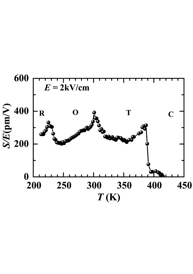
We then demonstrate that the system can be used to investigate the influence of phase transition on the piezoelectric response by using BTO ceramics as an example. To improve the insulation of BTO ceramics and obtain a good dielectric loop at high temperature, 2.5 mol% of Ti was substituted using Sn. Figure 7 shows the temperature dependence of dielectric and strain hysteresis loops under the application of a bipolar field, and the unipolar-field-driven strain at = 30 kV/cm, 10 kV/cm, and 2 kV/cm, respectively. As shown in Fig. 7, at = 423 K, BTO-Sn2.5% is in a nearly paraelectric state although a slightly nonlinear polarization appears at high electric field (the slight open polarization loop may be due to the leakage current). Therefore, the strain response is due to the electrostrictive effect, which is evident from the relationship of in the strain response. When the sample is cooled to temperatures close to the Curie point (= 380 K) such as = 393 K, the strain response is a mixture of the piezoelectric and electrostrictive effects owing to the appearance of local polarization in the sample. After a phase transition ( ), BTO-Sn2.5% is in a complete ferroelectric state, showing a typical butterfly strain loop for a bipolar field.
Figure 8 shows the temperature dependence of obtained at = 2 kV/cm. It can be seen that strain anomaly appears at the successive phase transitions in BTO-Sn2.5%. At the phase transition point, the strain response shows the maximum value. In addition, a larger strain response exists at temperatures of approximately within the cubic phase owing to the appearance of local polarization in the crystal. Similar phenomena have also been observed for the larger electric field of = 10 kV/cm and =30 kV/cm.
In summary, a capacitive displacement technique was developed, which allows measuring the electric-field-induced displacement in both bulk and film piezoelectric materials. The method can accurately determine an AC displacement of as small as 2 pm using a lock-in amplifier technique. It also allows measuring the large displacement within 25 m with a sub-nanometer resolution. Moreover, it can be used to investigate the strain variation within a temperature range of 210 - 450 K, allowing the temperature coefficient of the piezoelectric strain to be evaluated and the structure phase transition effects on the piezoelectric strain response to be studied. Experimental results on quartz, PZT ceramics and a thin film, and BaTiO3 ceramics confirm the capabilities of this technique.
Acknowledgements.
We thank Prof. H. Suzuki at Shizuoka University for providing the PZT thin film and Dr. R. Wang at AIST for providing the commercial PZT ceramics sample used for the examination of our system.DATA AVAILABILITY
The data supporting the findings of this study are available within this article.
References
- (1) J. Curie and P.Curie, Bull. Soc. Fr.Mineral. 3, 90 (1880).
- (2) B. Jaffe, W. R. Cook Jr., and H. Jaffe, Piezoelectric Ceramics (Academic, London, Great Britain, 1971).
- (3) M. E. Lines and A. M. Glass, Principle and Application of Ferroelectrics and Related materials (Clarendon, Oxford, Great Britain, 1977).
- (4) K. Uchino, Piezoelectric Actuators and Ultrasonic Motors (Kluwer Academic Publishers, Norwell, MA 1997).
- (5) P. Muralt, M. Kohli, T. Maeder, A. Kholkin, K. Brooks, N. Setter, and R. Luthier, Sensors and Actuators A 48, 157 (1995).
- (6) P. Muralt, Integrated Ferroelectrics 17, 297 (1997).
- (7) D. Damjanovic, Rep. Prog. Phys. 61, 1267 (1998).
- (8) D. L. DeVoe, Sensors and Actuators A 88, 263 (2001).
- (9) S. Zhang, F. Li, X. Jiang, J. Kim, J. Luo, and X. Geng, Prog. Mater. Sci. 68, 1 (2015).
- (10) M. Acosta, N. Novak, V. Rojas, S. Patel, R. Vaish, J. Koruza, G. A. Rossetti, and J. Rodel, Appl. Phys. Rev. 4, 041305 (2017).
- (11) S. Trolier-McKinstry,. S. Zhang, A. J. Bell, and X. Tan, Annu. Rev. Mater. Res. 48, 6 (2018).
- (12) H. Liu, J. Zhong, C. Lee, S.-W. Lee, and L. Lin, Appl. Phys. Rev. 5, 041306 (2018).
- (13) D. Fu, M. Endo, H. Taniguchi, T. Taniyama, and M. Itoh, Appl. Phys. Lett. 90, 252907 (2007).
- (14) D. Fu, M. Itoh, S. Koshihara, T. Kosugi, and S. Tsuneyuki, Phys. Rev. Lett. 100, 227601 (2008).
- (15) D. Fu, M. Itoh, and S. Koshihara, Appl. Phys. Lett. 93, 012903 (2008).
- (16) J. Rödel, W. Jo , K. T. P. Seifert, E. M. Anton, and T. Granzow, J. Am. Ceram. Soc. 92, 1153 (2009).
- (17) D. Fu, M. Endo, H. Taniguchi, T. Taniyama, M. Itoh, and S. Koshihara, J. Phys.: Condens. Matter. 23, 075901 (2011).
- (18) D. Fu, T. Arioka, H. Taniguchi, T. Taniyama, and M. Itoh, Appl. Phys. Lett. 99, 012904 (2011).
- (19) D. Fu, Y. Kamai, N. Sakamoto, N. Wakiya, H. Suzuki and M. Itoh, J. Phys.: Condens. Matter. 25, 425901 (2013).
- (20) IEEE standard on piezoelectricity. ANSI/IEEE Stand, 176-1987.
- (21) J. Fialka and P. Benes, IEEE Trans. Instrum. Meas. 62, 1047 (2013)
- (22) D. A. Berlincourt, J. Appl. Phys. 30,1804 (1959).
- (23) M. Stewart and M. G. Cain, Characterization of Ferroelectric Bulk Materials and Thin Films, M. G. Cain(Ed), (Springer, Dordrecht, 2014), 37-64.
- (24) V. E. Bottom, J. Appl. Phys. 41, 3941 (1970).
- (25) W. Y. Pan and L. E. Cross, Rev. Sci. Instrum. 60, 2071 (1989).
- (26) K. Lefki and G. J. M. Dormans, J. Appl. Phys. 76, 1764 (1994).
- (27) A. L. Kholkin, Ch. Wütchrich, D. V. Taylor, and N. Setter, Rev. Sci. Instrum. 67, 1935 (1996).
- (28) I. Kanno, S. Fujii, T. Kamada, and R. Takayama, Appl. Phys. Lett. 70, 1378 (1997).
- (29) J. A. Christman, R. R. Woolcott, Jr., A. I. Kingon, and R. J. Nemanich, Appl. Phys. Lett. 73, 3851 (1998).
- (30) F. Xu, F. Chu, and S. Trolier-McKinstry, J. Appl. Phys. 86, 588 (1999).
- (31) C. Durkan, D. P. Chu, P. Migliorato, and M. E. Welland, Appl. Phys. Lett. 76, 366 (2000).
- (32) O. Kuffer, I.Maggio-Aprile, J.-M. Triscone, O. Fischer, and Ch. Renner, Appl. Phys. Lett. 77, 1701 (2000).
- (33) D. Fu, K. Ishikawa, M. Minakata, and H. Suzuki, Jpn. J. Appl. Phys. 40, 5683 (2001).
- (34) G.-T. Park, J.-J. Choi, J. Ryu, H. Fan, and H.-E. Kim, Appl. Phys. Lett. 80, 4606 (2002).
- (35) G. M. Graham and F. N. D. D. Pereira, J. Appl. Phys. 42, 3011 (1971).
- (36) K. Uchino and L. E. Cross, Ferroelectrics 35, 3941 (1980).
- (37) A. S. Bhakka, D. N. Bose, E. W. White, and L. E. Cross, phys. stat. sol. (a) 7, 335 (1971).
- (38) N. Setter, D. Damjanovic, and L. Eng, J. Appl. Phys. 100, 051606 (2006).
- (39) David V. Taylor and D. Damjanovica, Appl. Phys. Lett. 76, 1615 (2000).
- (40) P. Gerber, A. Roelofs, O. Lohse, C. Kugeler, S. Tiedke, U. Bottger, and R. Waser, Rev. Sci. Instrum. 74, 2613 (2003).
- (41) Q. M. Zhang, H. Wang,N. Kim, and L. E. Cross, J. Appl. Phys. 75, 454 (1994).
- (42) M. Yokosuka, T. Ochiai, and M. Marutake, Jpn. J. Appl. Phys. 30, 2228 (1991).
- (43) S. Zhang, X. Dong, and S. Kojima, Jpn. J. Appl. Phys. 36, 2994 (1997).
- (44) R. G. Sabat, B. K. Mukherjee, W. Ren, and G. Yang, J. Appl. Phys. 101, 064111 (2007).
- (45) L. Burianova, P. Hana, M. Pustka, M. Prokopova, and J. Nosek, J. Euro. Ceram. Soc. 25, 2405 (2005).