Josephson junctions in double nanowires bridged by in-situ deposited superconductors
Abstract
We characterize parallel double quantum dot Josephson junctions based on closely-grown double nanowires bridged by in-situ deposited superconductors. The parallel double dot behavior occurs despite the closeness of the nanowires and the potential risk of nanowire clamping during growth. By tuning the charge filling and lead couplings, we map out the simplest parallel double quantum dot Yu-Shiba-Rusinov phase diagram. Our quasi-independent two-wire hybrids show promise for the realization of exotic topological phases.
I Introduction
Double Rashba-nanowires bridged by superconductors are at the center of proposals for qubitsAasen et al. (2016), coupled subgap statesYao et al. (2014) and exotic topological superconducting phases based on Majorana zero modes (MZMs)Béri and Cooper (2012); Altland and Egger (2013); Gaidamauskas et al. (2014); Klinovaja and Loss (2014); Ebisu et al. (2016); Schrade et al. (2017); Reeg et al. (2017); Schrade and Fu (2018); Thakurathi et al. (2018); Dmytruk et al. (2019); Thakurathi et al. (2020); Kotetes et al. (2019); Papaj et al. (2019); Haim and Oreg (2019). Researchers have theorized on the existence of a topological Kondo phase in such wires when the bridging superconductor is in Coulomb blockade Béri and Cooper (2012); Altland and Egger (2013); Galpin et al. (2014); Papaj et al. (2019) and, more recently, described a device hosting parafermions Klinovaja and Loss (2014). Concretion of these proposals should benefit from material science developments resulting in improved nanowire/superconductor interfaces with low quasiparticle poisoning rates Krogstrup et al. (2015); Albrecht et al. (2016); Higginbotham et al. (2015).
These clean interfaces have been used in the investigation of MZMs in single nanowires Deng et al. (2016); Albrecht et al. (2016) and, more recently, for coupling single and serial quantum dots (QDs) defined on single nanowires to superconductors to realize one and two-impurity Yu-Shiba-Rusinov (YSR) models Estrada Saldaña et al. (2018, 2020a); Valentini et al. (2020); Estrada Saldaña et al. (2020b); Razmadze et al. (2020). YSR excitations, sometimes referred to as Andreev bound states Buitelaar et al. (2002); Deacon et al. (2010a, b); Pillet et al. (2010); Lee et al. (2014); Jellinggaard et al. (2016); Li et al. (2017); Lee et al. (2017); Su et al. (2017); Gramich et al. (2017); Grove-Rasmussen et al. (2018); Estrada Saldaña et al. (2020a); Su et al. (2020); Estrada Saldaña et al. (2020b); Valentini et al. (2020); Prada et al. (2020), arise in the limit of large Coulomb charging energy, , where is the size of the superconducting gap, as a result of the virtual excitation of a quasiparticle into the edge of the superconducting gap Žitko et al. (2015); Kiršanskas et al. (2015). This quasiparticle can exchange-fluctuate with a localized spin in the QD, and if the exchange coupling is strong (i.e., when the Kondo temperature, , is larger than ), the ground state (GS) transits from a doublet to a singlet Satori et al. (1992). In Josephson junctions (JJs), this provokes a -0 phase-shift change in the superconducting phase difference Bauer et al. (2007); Rozhkov et al. (2001); Van Dam et al. (2006); Cleuziou et al. (2006); Grove-Rasmussen et al. (2007); Jørgensen et al. (2007); Eichler et al. (2009); De Franceschi et al. (2010); Maurand et al. (2012); Kim et al. (2013); Delagrange et al. (2015, 2018); Estrada Saldaña et al. (2018, 2020a); Meden (2019); Estrada Saldaña et al. (2019).
Devices which use pairs of QDs placed in a parallel configuration Baba et al. (2015); Deacon et al. (2015) and coupled to common superconducting leads have been extensively studied with the purpose of producing entangled electron states through Cooper pair splitting Hofstetter et al. (2009); Das et al. (2012); Baba et al. (2018); Ueda et al. (2019). However, the behaviour of the switching current, , in the presence of YSR screening Grove-Rasmussen et al. (2018); Estrada Saldaña et al. (2020a); Kürtössy et al. in parallel double QDs remains to be investigated.
In this work, we characterize superconductivity in closely-grown pairs of InAs nanowires bridged by a thin epitaxial superconducting aluminum film deposited in-situ Kanne et al. . To do so, we fabricate two side-by-side JJs out of one pair of nanowires and demonstrate that each nanowire hosts a single QD, through which supercurrent flows. From the charge stability diagram and magnetic field measurements, we establish that the interwire tunnelling is negligible with an upper bound of . The YSR physics is analyzed through the gate dependence of the linear conductance and , where we find that the common superconducting leads screen individually each QD, hinting at individual YSR clouds instead of a single one extending over the two QDs. We furthermore show indications of supercurrent interference when the ground-state parity of the QDs is different, reminiscent of a superconducting quantum interference device (SQUID) at zero magnetic field.
The article is structured in sections. In Section II, we introduce the YSR double QD phase diagram and measurements of two double QD shells in different coupling regimes are presented establishing weak interdot coupling. In Section III, we show signatures of interference between the supercurrents flowing through each junction. In Section IV, we demonstrate the YSR screening evolution of . Finally, in Section V we present our conclusions and provide perspectives of our work.
II Characterization of the parallel quantum-dot Josephson junction
In this section, we outline the device layout and demonstrate the Josephson effect and weak interdot tunnelling in Device 1. Data from an additional device (Device 2) is shown in Supplemental Material (SM).
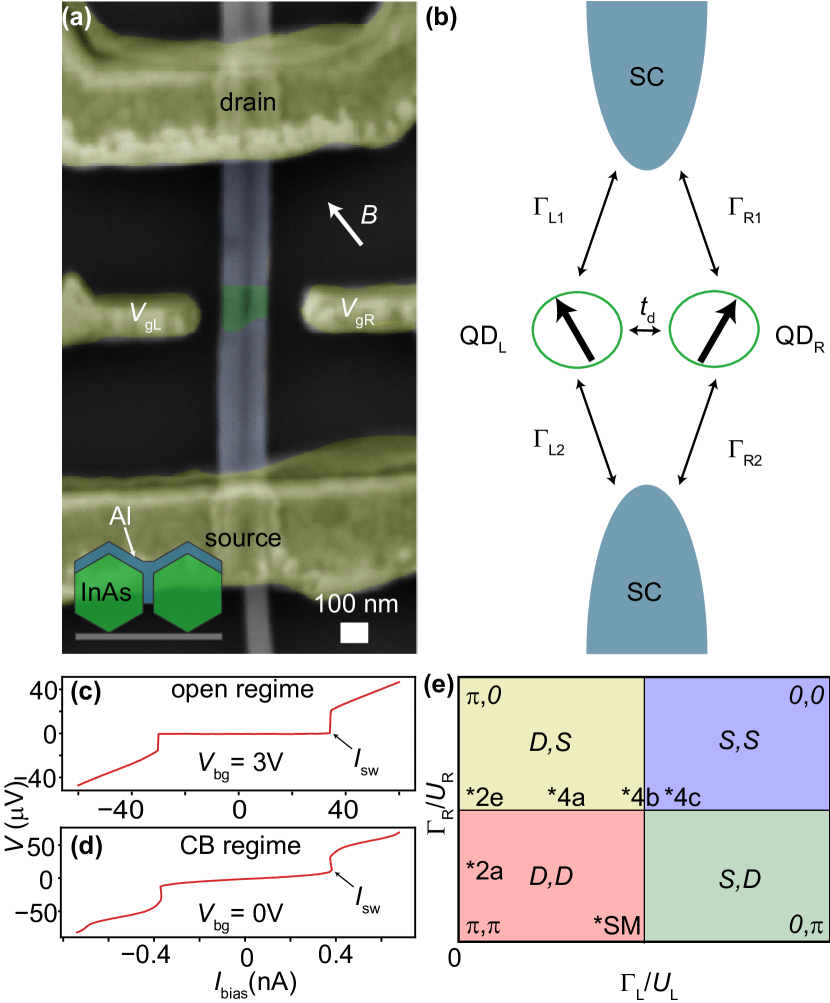
Figure 1a shows a falsely-colored scanning electron microscopy (SEM) image of Device 1. Two 80-nm InAs nanowires (in green), grown close to each other in a molecular beam epitaxy chamber, and covered each on three of its facets by an in-situ deposited 17 nm-thick layer of aluminum (in blue)Kanne et al. , are individually picked with a micromanipulator and deposited on a Si/SiOx substrate. A resist mask is defined by electron beam lithography to selectively etch Al using the commercial etchant Transene-D, creating a parallel double JJ with 100 nm-wide bare sections of the two nanowires as weak links. Ti/Au 5 nm/250 nm-thick contacts to Al and individual nanowire side-gates are deposited after a subsequent lithography step. Prior to the metal deposition step and without breaking vacuum, the Al native oxide is removed by argon milling to establish a good contact. The devices are measured in a dilution refrigerator at base temperature .
QDs are formed when the two nanowires are brought near depletion with the use of the individual side-gate voltages, and , and a global backgate voltage, . The side gates are also used as plunger gates of the QDs. In Fig. 1b, we sketch the tunnelling rates of the QDs to the common superconducting leads (SC), , , , and , which can vary among different shells of the QDs and which can also be tuned by . The QDs may also be coupled to each other by an interdot tunnel coupling, . We identify these different shells by the letters W, X, Y. QD parameters extracted for these shells are given in Table 1. For an overview of the different shells explored, see SM, Section I.
The source and the drain contacts of the device each branch out into two leads as shown in Fig. 1a, which we use to characterize the parallel JJs Guiducci et al. (2019) in a four-terminal configuration by applying a current, , from source to drain leads and measuring the voltage response, , in a different pair of source and drain leads. In this way, we obtain curves which switch from a supercurrent branch at low to a high-slope dissipative branch at . Two of such curves are shown in Fig. 1c,d for the open and Coulomb blockaded regimes, respectively. We measure up to 35 nA in the former regime and up to approximately 500 pA in the latter regime. In Coulomb blockade, the supercurrent branch shows a finite slope, , which increases with ; however, this does not affect our identification of as a jump in the curve down to 5 pA (see SM, Section II). In our analysis below (Sec. III) we do not claim quantitative estimates of the critical current, (which may be larger), but only address the qualitative behavior of .
As a guide to the different GS configurations accessed in this work, we show in Fig. 1e a sketch of the phase diagram of the parallel DQD JJ versus coupling to the leads when the two QDs have independent GSs (). The sketch corresponds to odd occupancy (1,1) of the QDs and it is valid for the large level-spacing regime, , where i stands for left and right QDs. The independent-GS case is applicable to our device as most measurements are done away from the triple points of the QDs, where the effect of a finite is negligible. GS changes occur when the total tunnelling rates of each of the QDs to the common superconducting leads surpass a threshold which depends on Lee et al. (2014), where is the superconducting gap. Above this threshold, the spin of each QD is individually screened by the superconducting leads via the YSR mechanism Žitko et al. (2011); Yao et al. (2014). For doublet GS, the current-phase relationship is -shifted, e.g. Jørgensen et al. (2007); Van Dam et al. (2006); Maurand et al. (2012); Cleuziou et al. (2006) as indicated in Fig. 1e.
| Shell | ||||||||||
|---|---|---|---|---|---|---|---|---|---|---|
| W | ||||||||||
| X | ||||||||||
| Y |
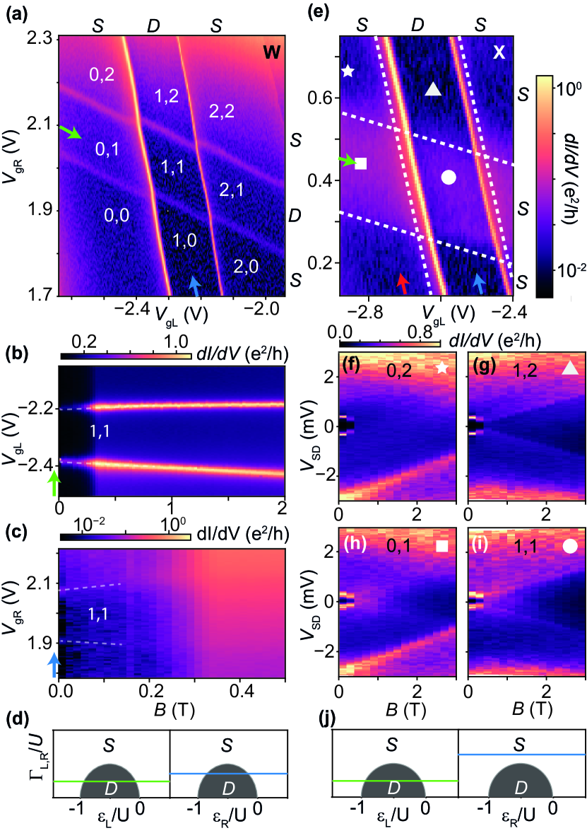
To estimate , we first investigate via two-terminal voltage-biased differential conductance () measurements two shells corresponding to the two leftmost quadrants of the DQD phase diagram in Fig. 1e. The two-terminal is recorded using standard lock-in amplifier techniques with an AC excitation of 2 . Figure 2a shows a colormap of at source-drain bias of shell W in the superconducting state versus and , which represents the stability diagram of the two QDs in the weakly-coupled regime where (see Table 1 for shell parameters). Since the slope of the supercurrent branch, , is empirically related in our device to , we can use as an indicator of . This is particularly relevant in the Coulomb-blockade regime, when is small and is significant (see SM, Section II). We observe approximately vertical and horizontal conductance lines which overlap and displace each other at their crossings, without exhibiting any significant bending. The displacement is a signature of a finite interdot charging energy, while the lack of bending indicates that (with an upper limit of 10 V based on the width of the sharpest conductance lines). No signatures of CAR or of elastic co-tunnellingScherübl et al. (2020) are observed in this measurement. We interpret these lines as GS parity transition lines, which indicate changes of parity in the left and right QDs, respectively. The lines separate nine different and well-defined parity sectors. We assign corresponding effective left and right QD charges, , to each of these sectors based on the shell-filling pattern of the stability diagram in larger plunger-gate ranges (see SM, Section I). The charges obtained in this way are indicated in Fig. 2a.
To assign GS parities to these nine sectors, and to determine independently if, in addition to interdot charging energy, there is a significant , we trace the evolution of the parity transition lines of the 1,1 charge sector against . In the case of singlet GS; i.e., when the spins of the two QDs are exchange-coupled (finite ), these lines are expected to come together with . Instead, as shown in the zero-bias colormaps in Figs. 2b,c, the parity transition lines enclosing the 1,1 charge sector split apart with , i.e., the two QDs are independent doublets, despite the relative closeness of the two nanowires. The splitting of the parity lines occurs both in the case when the parity of the left (right) QD is varied and the right (left) QD is kept in the doublet GS (see green and blue arrow, respectively, in Fig. 2a). The GS (singlet or doublet ) of the other eight charge sectors are indicated on the top and right exterior parts of the stability-diagram colormap in Fig. 2a.
Given the decoupling between the two QDs, we can approximate their phase diagrams by those of two independent single QDs. Neglecting the interdot charging energy, we sketch in Fig. 2d the well-known single-QD phase diagrams for the GS of the left and right QDs versus QD level position, , and versus the total tunnelling rate of each QD to the leads, , over their charging energy, . The doublet dome has an upper height limit of in the infinite limit, and its height decreases in the limit (i.e., the YSR regime) to which our QDs belong Meng et al. (2009); Lee et al. (2017). In the left phase diagram, the horizontal green line which crosses the doublet dome indicates a cut where is varied and is kept fixed such that the GS parity of the right QD is a doublet, and the GS parity of the left QD is variable. This line represents schematically the gate trajectory in Fig. 2b, as indicated with the green arrow, which is collinear to the green arrow in Fig. 2a, and which varies the parity of the left QD as -- while keeping the parity of the right QD as . A similar relation exists between the horizontal blue line in the right phase diagram, and the gate trajectory (blue arrow) in Fig. 2c, also collinear to the corresponding arrow in Fig. 2a. From these phase diagrams, we note that parity transitions are strictly equal to Coulomb degeneracies only at zero ). The measurements above confirm the expected DQD behavior for low lead couplings, which shows a , ground for charge state 1,1 corresponding to the lower left quadrant of the phase diagram in Fig. 1e.
Next, we investigate a differently coupled shell (shell X) which belongs to the upper left quadrant of phase diagram in Fig. 1e. Figure 2e shows the zero-bias colormap in the superconducting state vs. the plunger gates of the two QDs of shell X. The two horizontal GS-parity transition lines, which bounded the green trajectory in the case of shell W, are absent in the case of shell X, and are instead replaced by a band of enhanced conductance. The conductance band is cut two times by approximately vertical conductance lines, which correspond to GS-parity transition lines of the left QD.
The parity of the band of enhanced conductance in the stability diagram is determined from the -evolution of the differential conductance in the normal state versus at two fixed gate voltages. These two gate voltages are indicated by a square (charge states 0,1) and a circle (1,1) in the stability diagram, and their dependence is respectively shown in Figs. 2h,i. As a control experiment, the dependence for two fixed gate voltages above the conductance band indicated by a star (0,2) and a triangle (1,2) in the stability diagram, is shown in Figs. 2f,g. The four measurements show closing of the superconducting gap at T, which is consistent with the jump in the zero-bias signal in Figs. 2b,c at T. However, in the normal state, whereas Figs. 2g-i (1,2 0,1 1,1) display conductance steps near zero-bias which split with field, in Fig. 2f there is no such splitting, consistent with even filling of both dots. We assign effective QD charge numbers to the charge stability diagram from a T measurement (see SM, Section III) and overlay the Coulomb lines obtained, which delimit the nine charge sectors (white dashed lines in Fig. 2e).
We note an additional important difference in the data of the low-bias splitting states. Whereas in Fig. 2g (1,2) the splitting can be traced back to zero bias at , in Fig. 2h (0,1) the splitting is traced to zero bias only at a finite field of T. The pair of features whose splitting can be traced to a onset in Fig. 2g (1,2) correspond to co-tunnelling steps of the odd-occupied left QD experiencing Zeeman splitting. In turn, the pair of features which starts to split at 1 T in Fig. 2h corresponds to the Zeeman splitting of a Kondo resonance in the right QD. The splitting ensues when .Kogan et al. (2004) Notice that the Kondo resonance is also visible in the data after the gap closure at . From the splitting, we find a -factor . Table 1 shows that for shell X, which is consistent with a YSR singlet state in the right QD in the superconducting state.
The -dependence data in Figs. 2f-i therefore allows us to assign the GS to the QDs, or , in each of the nine sectors in Fig. 2e. We indicate schematically by a green and blue horizontal line in the two individual-QD phase-diagram cartoons in Fig. 2j the GS along the gate trajectories collinear to the same-colored arrows in the colormap of Fig. 2e. The green (blue) gate trajectory, which goes along (perpendicular to) the band of enhanced conductance intersects twice (goes above) the doublet dome, leading to two (zero) parity transitions.
III Supercurrent interference for different quantum-dot parities
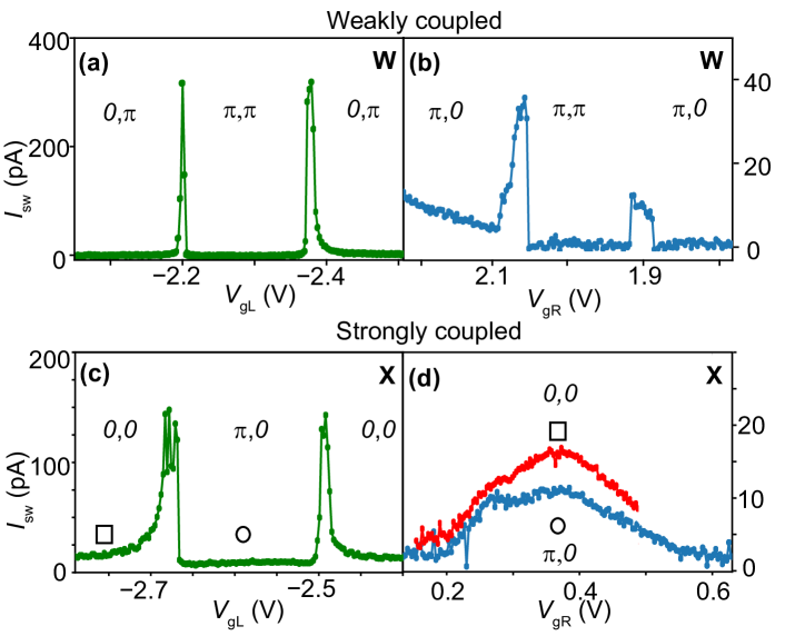
We switch back to the four-terminal measurement configuration to correlate the intrinsic phase of each JJ with the magnitude of . In Fig. 3, we show versus plunger gate voltages, where is extracted in a similar fashion as in Fig. 1d. In Figs. 3a,c (3b,d), the plunger gate voltages are swept along trajectories which vary the occupation in the left (right) QD while keeping the occupation of the right (left) QD fixed, following the green (red, blue) arrows in Figs. 2a,e, i.e. for shell W and X, respectively. For reference, we assign the expected phase-shift in the current-phase relationship, or 0, based on the measured GS parities of the two QDs. This phase-shift is accurate when at least one QD is in Coulomb blockade. The value of at the parity transitions may include contribution due to presence of bound states crossing zero-energy. Hence, the magnitude of on transitions should not be taken into account.
The common phenomenology in the data is as follows. After a smooth build-up of towards a transition, the current abruptly drops right at the edge of the domain, resulting in an asymmetric peak Jørgensen et al. (2007). A pair of asymmetric peaks is seen in the data in Figs. 3a-c, as one of the QDs experiences parity transitions and therefore a sequence of phase-shift changes. If the parity stays unchanged, such peaks are absent, as in Fig. 3d. Instead, is smoothly enhanced towards odd occupation of the right QD, which is YSR-screened (i.e., ) Maurand et al. (2012). Interestingly, when comparing the red and blue traces in Fig. 3d, which correspond to different phase shift ( and 0, respectively) in the JJ formed by the left QD, we observe that is stronger near V. Note that V corresponds to the 1,1 charge state for the blue trace, and to the 0,1 charge state for the red trace. The exact magnitude of in that gate value for the red and blue curve is consistent with what is found in Fig. 3c in the () and () respectively. We can interpret the reduction in at V in the blue trace with respect to the red trace by considering the double nanowire device as a SQUID at zero threaded magnetic flux Cleuziou et al. (2006); Van Dam et al. (2006); Maurand et al. (2012). The of a SQUID with a sinusoidal current-phase relation can be written as Maurand et al. (2012)
| (1) |
where are the critical currents of the two JJs, is the threaded magnetic flux and are the intrinsic phase shifts (0 or ) of the junctions. As a result, for the total is given by when the DQD is in the 0,0 phase, and in the ,0 phase. These equations may explain the findings in Fig. 3c,d, as is enhanced when both JJs have the same intrinsic phase, and it is weaker when the two JJs have different phase.
IV Screening evolution of switching current
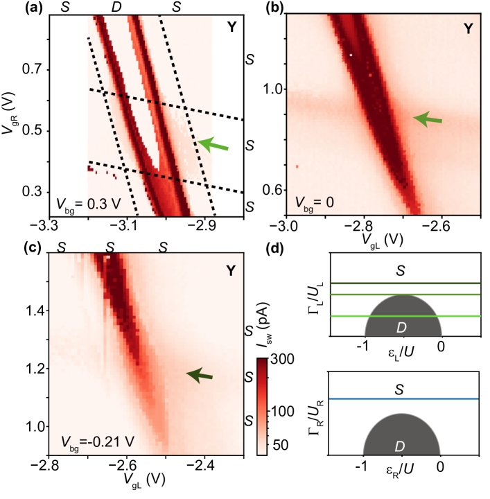
Finally, we demonstrate individual control of the couplings between the SC leads and the QDs, realizing the transition from the upper left (one screened spin in 1,1) to upper right quadrant (both spins screened) in the YSR phase diagram depicted in Fig. 1e. Whereas the changes in GS parity in Fig. 2 occurred primarily by changing the side-gate voltages to go from shell W to shell X, here the changes occur within a unique shell. This is done in a shell identified as Y, using as a tuning knob of . In Figs. 4a-c, we show colormaps representing parity stability diagrams at different analogous to those in Figs. 2a,e; however, instead of plotting a measurement of voltage-biased , we directly plot a four-terminal measurement of vs. plunger-gate voltages. To obtain each colormap, we measure the characteristic at each plunger gate voltage coordinate (i.e., at each pixel in the colormap) and extract as in the example in Fig. 1d.
In Fig. 4a, the parity stability diagram shows two peaks which correspond to two parity transitions of the left QD. The lack of right-QD parity transition lines indicates that the right QD is YSR-screened. We corroborate that this is indeed the case from a measurement of at T in the normal state, and we find (see Table 1). We also note that, although faintly-visible here, a two-terminal measurement of the stability diagram in otherwise the same conditions as here displays an horizontal band of (weakly) enhanced conductance, which is the same phenomenology identified in Fig. 2d with YSR spin-screening. However, the enhancement is weak enough to preclude resolution of , and therefore a similar band of does only show at the right part of Fig. 4a ( V, V).
Reducing alters the parity stability diagram by bringing the two peaks (parity lines) of the left QD closer together, as shown in Fig. 4b. Note that a faint, approximately horizontal band of is observed along the direction pointed by the dark-green arrow, which comes as a result of enhancement of due to YSR spin-screening of the right QD. In Fig. 4c, further reduction of leads to merging of the parity lines into a vertical band of across the whole plot. At this point, the spins of both QDs are YSR-screened into singlets. We have therefore traced the phase diagram shown in Fig. 1e, where either one spin of a QD or both are screened by the YSR mechanism, triggering a phase change in the current-phase relation of the JJs. Additional data on the magnetic field dependence of this shell can be found in the SM, section IV.
V Conclusions & Outlook
In conclusion, we have demonstrated parallel quantum-dot Josephson junctions fabricated out of a double-nanowire platform in which the nanowires are bridged by an in-situ deposited superconductor. We mapped out the parallel quantum dot YSR phase diagram via conductance and switching current measurements showing the tunability of the ground state of each JJ from doublet to singlet. The analysis also revealed that the nanowires are predominantly decoupled with an upper bound on the interwire/dot tunnel coupling in the order of eV for the specific charge states studied in two devices. Finally, we showed indications of switching current addition and subtraction via appropriate choice of ground states of the two dots involving the YSR singlet state, i.e., and (phase difference) regimes, respectively.
The above observations of basic superconducting properties in in-situ made hybrid double nanowire material open up for more advanced experiments addressing a number of recent theoretical proposals. In parallel double-quantum-dot Cooper-pair splitters Hofstetter et al. (2009); Herrmann et al. (2010), the CAR mechanism responsible for the splitting is weakened by an increase in the distance between the tunnelling points from the superconductor into the two quantum dots Recher et al. (2001). The closeness of the nanowires set by growthKanne et al. and the cleanness of the Al-InAs interface may turn out beneficial for CAR, which is also the basis for creating coupled YSR states in these systems Yao et al. (2014); Scherübl et al. (2019). The latter is investigated in a parallel work on the same hybrid double nanowire materialKanne et al. as used in this workKürtössy et al. . The hybrid double nanowires are furthermore interesting for realizing several species of topological subgap statesGaidamauskas et al. (2014); Klinovaja and Loss (2014). For finite CAR, the requirements for entering the topological regime hosting Majorana bound states have been shown to be lowered Schrade et al. (2017); Dmytruk et al. (2019), and parafermions may be achieved in a regime where CAR dominates over local Andreev processesKlinovaja and Loss (2014). In superconducting islands fabricated in our hybrid double nanowires, the topological Kondo effect may be pursuedBéri and Cooper (2012); Altland and Egger (2013); Papaj et al. (2019). In double-nanowire Josephson junctions as here demonstrated, however, in the topological regime, non-standard types of Andreev bound states have been predicted Kotetes et al. (2019). As an ending remark, we note that double nanowires can also be made with a full superconducting shell Kanne et al. ; Vekris et al. , relevant for investigating flux-induced subgap statesValentini et al. (2020); Vaitiekėnas et al. (2020); Peñaranda et al. (2020).
VI Acknowledgements
We thank Gorm Steffensen, Jens Paaske, Michele Burrello and Constantin Schrade for useful discussions. We thank Xinyan Wang for experimental contribution. We acknowledge the support of the Sino-Danish Center, the European Union’s Horizon 2020 research and innovation program under the Marie Sklodowska-Curie Grant Agreement No. 832645, QuantERA “SuperTop” (NN 127900), the European Union’s Horizon 2020 research and innovation programme FETOpen Grant No. 828948 (AndQC), the Danish National Research Foundation, Villum Foundation Project No. 25310, the Ministry of Science and Technology of China through the National Key Research and Development Program of China (Grant Nos. 2017YFA0303304, 2016YFA0300601), the National Natural Science Foundation of China (Grant No. 11874071), the Beijing Academy of Quantum Information Sciences (Grant No. Y18G22), Carlsberg Foundation and the Independent Research Fund Denmark.
References
- Aasen et al. (2016) D. Aasen, M. Hell, R. V. Mishmash, A. Higginbotham, J. Danon, M. Leijnse, T. S. Jespersen, J. A. Folk, C. M. Marcus, K. Flensberg, and J. Alicea, Phys. Rev. X 6, 031016 (2016).
- Yao et al. (2014) N. Y. Yao, C. P. Moca, I. Weymann, J. D. Sau, M. D. Lukin, E. A. Demler, and G. Zaránd, Phys. Rev. B 90, 241108 (2014).
- Béri and Cooper (2012) B. Béri and N. R. Cooper, Phys. Rev. Lett. 109, 156803 (2012).
- Altland and Egger (2013) A. Altland and R. Egger, Phys. Rev. Lett. 110, 196401 (2013).
- Gaidamauskas et al. (2014) E. Gaidamauskas, J. Paaske, and K. Flensberg, Phys. Rev. Lett. 112, 126402 (2014).
- Klinovaja and Loss (2014) J. Klinovaja and D. Loss, Phys. Rev. B 90, 045118 (2014).
- Ebisu et al. (2016) H. Ebisu, B. Lu, J. Klinovaja, and Y. Tanaka, Progress of Theoretical and Experimental Physics 2016 (2016), 10.1093/ptep/ptw094, 083I01.
- Schrade et al. (2017) C. Schrade, M. Thakurathi, C. Reeg, S. Hoffman, J. Klinovaja, and D. Loss, Phys. Rev. B 96, 035306 (2017).
- Reeg et al. (2017) C. Reeg, J. Klinovaja, and D. Loss, Phys. Rev. B 96, 081301 (2017).
- Schrade and Fu (2018) C. Schrade and L. Fu, Phys. Rev. Lett. 120, 267002 (2018).
- Thakurathi et al. (2018) M. Thakurathi, P. Simon, I. Mandal, J. Klinovaja, and D. Loss, Phys. Rev. B 97, 045415 (2018).
- Dmytruk et al. (2019) O. Dmytruk, M. Thakurathi, D. Loss, and J. Klinovaja, Phys. Rev. B 99, 245416 (2019).
- Thakurathi et al. (2020) M. Thakurathi, D. Chevallier, D. Loss, and J. Klinovaja, Phys. Rev. Research 2, 023197 (2020).
- Kotetes et al. (2019) P. Kotetes, M. T. Mercaldo, and M. Cuoco, Phys. Rev. Lett. 123, 126802 (2019).
- Papaj et al. (2019) M. Papaj, Z. Zhu, and L. Fu, Phys. Rev. B 99, 014512 (2019).
- Haim and Oreg (2019) A. Haim and Y. Oreg, Physics Reports 825, 1 (2019).
- Galpin et al. (2014) M. R. Galpin, A. K. Mitchell, J. Temaismithi, D. E. Logan, B. Béri, and N. R. Cooper, Phys. Rev. B 89, 045143 (2014).
- Krogstrup et al. (2015) P. Krogstrup, N. L. B. Ziino, W. Chang, S. M. Albrecht, M. H. Madsen, E. Johnson, J. Nygård, C. M. Marcus, and T. S. Jespersen, Nat. Mater. 14, 400 (2015).
- Albrecht et al. (2016) S. M. Albrecht, A. P. Higginbotham, M. Madsen, F. Kuemmeth, T. S. Jespersen, J. Nygård, P. Krogstrup, and C. M. Marcus, Nature 531, 206 (2016).
- Higginbotham et al. (2015) A. P. Higginbotham, S. M. Albrecht, G. Kiršanskas, W. Chang, F. Kuemmeth, P. Krogstrup, T. S. Jespersen, J. Nygård, K. Flensberg, and C. M. Marcus, Nature Physics 11, 1017 (2015).
- Deng et al. (2016) M. T. Deng, S. Vaitiekėnas, E. B. Hansen, J. Danon, M. Leijnse, K. Flensberg, J. Nygård, P. Krogstrup, and C. M. Marcus, Science 354, 1557 (2016).
- Estrada Saldaña et al. (2018) J. C. Estrada Saldaña, A. Vekris, G. Steffensen, R. Žitko, P. Krogstrup, J. Paaske, K. Grove-Rasmussen, and J. Nygård, Phys. Rev. Lett. 121, 257701 (2018).
- Estrada Saldaña et al. (2020a) J. C. Estrada Saldaña, A. Vekris, R. Žitko, G. Steffensen, P. Krogstrup, J. Paaske, K. Grove-Rasmussen, and J. Nygård, Phys. Rev. B 102, 195143 (2020a).
- Valentini et al. (2020) M. Valentini, F. Peñaranda, A. Hofmann, M. Brauns, R. Hauschild, P. Krogstrup, P. San-Jose, E. Prada, R. Aguado, and G. Katsaros, arXiv (2020), 2008.02348 .
- Estrada Saldaña et al. (2020b) J. C. Estrada Saldaña, A. Vekris, V. Sosnovtseva, T. Kanne, P. Krogstrup, K. Grove-Rasmussen, and J. Nygård, Commun. Phys. 3, 1 (2020b).
- Razmadze et al. (2020) D. Razmadze, E. C. T. O’Farrell, P. Krogstrup, and C. M. Marcus, Phys. Rev. Lett. 125, 116803 (2020).
- Buitelaar et al. (2002) M. R. Buitelaar, T. Nussbaumer, and C. Schönenberger, Phys. Rev. Lett. 89, 256801 (2002).
- Deacon et al. (2010a) R. S. Deacon, Y. Tanaka, A. Oiwa, R. Sakano, K. Yoshida, K. Shibata, K. Hirakawa, and S. Tarucha, Phys. Rev. Lett. 104, 076805 (2010a).
- Deacon et al. (2010b) R. S. Deacon, Y. Tanaka, A. Oiwa, R. Sakano, K. Yoshida, K. Shibata, K. Hirakawa, and S. Tarucha, Phys. Rev. B 81, 121308 (2010b).
- Pillet et al. (2010) J.-D. Pillet, C. H. L. Quay, P. Morfin, C. Bena, A. L. Yeyati, and P. Joyez, Nat. Phys. 6, 965 (2010).
- Lee et al. (2014) E. J. H. Lee, X. Jiang, M. Houzet, R. Aguado, C. M. Lieber, and S. De Franceschi, Nat. Nanotechnol. 9, 79 (2014).
- Jellinggaard et al. (2016) A. Jellinggaard, K. Grove-Rasmussen, M. H. Madsen, and J. Nygård, Phys. Rev. B 94, 064520 (2016).
- Li et al. (2017) S. Li, N. Kang, P. Caroff, and H. Q. Xu, Phys. Rev. B 95, 014515 (2017).
- Lee et al. (2017) E. J. H. Lee, X. Jiang, R. Žitko, R. Aguado, C. M. Lieber, and S. De Franceschi, Phys. Rev. B 95, 180502 (2017).
- Su et al. (2017) Z. Su, A. B. Tacla, M. Hocevar, D. Car, S. R. Plissard, E. P. A. M. Bakkers, A. J. Daley, D. Pekker, and S. M. Frolov, Nat. Commun. 8, 1 (2017).
- Gramich et al. (2017) J. Gramich, A. Baumgartner, and C. Schönenberger, Phys. Rev. B 96, 195418 (2017).
- Grove-Rasmussen et al. (2018) K. Grove-Rasmussen, G. Steffensen, A. Jellinggaard, M. H. Madsen, R. Žitko, J. Paaske, and J. Nygård, Nature communications 9, 1 (2018).
- Su et al. (2020) Z. Su, R. Žitko, P. Zhang, H. Wu, D. Car, S. R. Plissard, S. Gazibegovic, G. Badawy, M. Hocevar, J. Chen, E. P. A. M. Bakkers, and S. M. Frolov, Phys. Rev. B 101, 235315 (2020).
- Prada et al. (2020) E. Prada, P. San-Jose, M. W. A. de Moor, A. Geresdi, E. J. H. Lee, J. Klinovaja, D. Loss, J. Nygård, R. Aguado, and L. P. Kouwenhoven, Nat. Rev. Phys. 2, 575 (2020).
- Žitko et al. (2015) R. Žitko, J. S. Lim, R. López, and R. Aguado, Phys. Rev. B 91, 045441 (2015).
- Kiršanskas et al. (2015) G. Kiršanskas, M. Goldstein, K. Flensberg, L. I. Glazman, and J. Paaske, Phys. Rev. B 92, 235422 (2015).
- Satori et al. (1992) K. Satori, H. Shiba, O. Sakai, and Y. Shimizu, J. Phys. Soc. Jpn. 61, 3239 (1992).
- Bauer et al. (2007) J. Bauer, A. Oguri, and A. C. Hewson, J. Phys.: Condens. Matter 19, 486211 (2007).
- Rozhkov et al. (2001) A. V. Rozhkov, D. P. Arovas, and F. Guinea, Phys. Rev. B 64, 233301 (2001).
- Van Dam et al. (2006) J. A. Van Dam, Y. V. Nazarov, E. P. Bakkers, S. De Franceschi, and L. P. Kouwenhoven, Nature 442, 667 (2006).
- Cleuziou et al. (2006) J.-P. Cleuziou, W. Wernsdorfer, V. Bouchiat, T. Ondarçuhu, and M. Monthioux, Nat. Nanotechnol. 1, 53 (2006).
- Grove-Rasmussen et al. (2007) K. Grove-Rasmussen, H. I. Jørgensen, and P. E. Lindelof, New J. Phys. 9, 124 (2007).
- Jørgensen et al. (2007) H. I. Jørgensen, T. Novotný, K. Grove-Rasmussen, K. Flensberg, and P. E. Lindelof, Nano Lett. 7, 2441 (2007).
- Eichler et al. (2009) A. Eichler, R. Deblock, M. Weiss, C. Karrasch, V. Meden, C. Schönenberger, and H. Bouchiat, Phys. Rev. B 79, 161407 (2009).
- De Franceschi et al. (2010) S. De Franceschi, L. Kouwenhoven, C. Schönenberger, and W. Wernsdorfer, Nat. Nanotechnol. 5, 703 (2010).
- Maurand et al. (2012) R. Maurand, T. Meng, E. Bonet, S. Florens, L. Marty, and W. Wernsdorfer, Phys. Rev. X 2, 011009 (2012).
- Kim et al. (2013) B.-K. Kim, Y.-H. Ahn, J.-J. Kim, M.-S. Choi, M.-H. Bae, K. Kang, J. S. Lim, R. López, and N. Kim, Phys. Rev. Lett. 110, 076803 (2013).
- Delagrange et al. (2015) R. Delagrange, D. J. Luitz, R. Weil, A. Kasumov, V. Meden, H. Bouchiat, and R. Deblock, Phys. Rev. B 91, 241401 (2015).
- Delagrange et al. (2018) R. Delagrange, R. Weil, A. Kasumov, M. Ferrier, H. Bouchiat, and R. Deblock, Physica B 536, 211 (2018).
- Meden (2019) V. Meden, J. Phys.: Condens. Matter 31, 163001 (2019).
- Estrada Saldaña et al. (2019) J. C. Estrada Saldaña, R. Žitko, J. P. Cleuziou, E. J. H. Lee, V. Zannier, D. Ercolani, L. Sorba, R. Aguado, and S. De Franceschi, Sci. Adv. 5, eaav1235 (2019).
- Baba et al. (2015) S. Baba, J. Sailer, R. S. Deacon, A. Oiwa, K. Shibata, K. Hirakawa, and S. Tarucha, Applied Physics Letters 107, 222602 (2015), arXiv:1512.02344 [cond-mat.supr-con] .
- Deacon et al. (2015) R. S. Deacon, A. Oiwa, J. Sailer, S. Baba, Y. Kanai, K. Shibata, K. Hirakawa, and S. Tarucha, Nat. Commun. 6, 1 (2015).
- Hofstetter et al. (2009) L. Hofstetter, S. Csonka, J. Nygård, and C. Schönenberger, Nature 461, 960 (2009).
- Das et al. (2012) A. Das, Y. Ronen, M. Heiblum, D. Mahalu, A. V. Kretinin, and H. Shtrikman, Nat. Commun. 3, 1 (2012).
- Baba et al. (2018) S. Baba, C. Jünger, S. Matsuo, A. Baumgartner, Y. Sato, H. Kamata, K. Li, S. Jeppesen, L. Samuelson, H. Q. Xu, C. Schönenberger, and S. Tarucha, New J. Phys. 20, 063021 (2018).
- Ueda et al. (2019) K. Ueda, S. Matsuo, H. Kamata, S. Baba, Y. Sato, Y. Takeshige, K. Li, S. Jeppesen, L. Samuelson, H. Xu, and S. Tarucha, Sci. Adv. 5, eaaw2194 (2019).
- (63) O. Kürtössy, Z. Scherübl, G. Fülöp, I. Endre Lukács, P. Makk, J. Nygård, and S. Csonka, arXiv:2103.14083 .
- (64) T. Kanne, D. Olsteins, M. Marnauza, A. Vekris, J. C. Estrada Saldaña, S. Loric̀, R. D.S̃chlosser, D. Ross, S. Csonka, K. Grove-Rasmussen, and J. Nygård, arXiv:2103.13938 .
- Guiducci et al. (2019) S. Guiducci, M. Carrega, F. Taddei, G. Biasiol, H. Courtois, F. Beltram, and S. Heun, Phys. Rev. B 99, 235419 (2019).
- Žitko et al. (2011) R. Žitko, O. Bodensiek, and T. Pruschke, Phys. Rev. B 83, 054512 (2011).
- Scherübl et al. (2020) Z. Scherübl, G. Fülöp, C. P. Moca, J. Gramich, A. Baumgartner, P. Makk, T. Elalaily, C. Schönenberger, J. Nygård, G. Zaránd, and S. Csonka, Nat. Commun. 11, 1 (2020).
- Meng et al. (2009) T. Meng, S. Florens, and P. Simon, Phys. Rev. B 79, 224521 (2009).
- Kogan et al. (2004) A. Kogan, S. Amasha, D. Goldhaber-Gordon, G. Granger, M. A. Kastner, and H. Shtrikman, Phys. Rev. Lett. 93, 166602 (2004).
- Herrmann et al. (2010) L. G. Herrmann, F. Portier, P. Roche, A. L. Yeyati, T. Kontos, and C. Strunk, Phys. Rev. Lett. 104, 026801 (2010).
- Recher et al. (2001) P. Recher, E. V. Sukhorukov, and D. Loss, Phys. Rev. B 63, 165314 (2001).
- Scherübl et al. (2019) Z. Scherübl, A. Pályi, and S. Csonka, Beilstein J. Nanotechnol. 10, 363 (2019).
- (73) A. Vekris, J. C. Estrada Saldaña, J. de Bruijckere, S. Loric̀, T. Kanne, M. Marnauza, D. Olsteins, J. Nygård, and K. Grove-Rasmussen, preprint .
- Vaitiekėnas et al. (2020) S. Vaitiekėnas, G. W. Winkler, B. van Heck, T. Karzig, M.-T. Deng, K. Flensberg, L. I. Glazman, C. Nayak, P. Krogstrup, R. M. Lutchyn, and C. M. Marcus, Science 367, eaav3392 (2020).
- Peñaranda et al. (2020) F. Peñaranda, R. Aguado, P. San-Jose, and E. Prada, Phys. Rev. Research 2, 023171 (2020).