Topological charge density waves at half-integer filling of a moiré superlattice
At partial filling of a flat band, strong electronic interactions may favor gapped states harboring emergent topology with quantized Hall conductivity. Emergent topological states have been found in partially filled Landau levels Tsui et al. (1982) and Hofstadter bands Wang et al. (2015); Spanton et al. (2018); in both cases, a large magnetic field is required to engineer the underlying flat band. The recent observation of quantum anomalous Hall effects (QAH) in narrow band moiré systems Chen et al. (2020a); Serlin et al. (2020); Stepanov et al. (2020); Polshyn et al. (2020) has led to the theoretical prediction that such phases may be realized even at zero magnetic field Zhang et al. (2019); Ledwith et al. (2020); Repellin and Senthil (2020); Abouelkomsan et al. (2020); Wilhelm et al. (2021). Here we report the experimental observation of insulators with Chern number in the zero magnetic field limit at and filling of the moiré superlattice unit cell in twisted monolayer-bilayer graphene (tMBG) Polshyn et al. (2020); Chen et al. (2020b); Xu et al. (2021); He et al. (2021). Our observation of Chern insulators at half-integer values of suggests spontaneous doubling of the superlattice unit cell, in addition to spin- and valley-ferromagnetism Kumar et al. (2014); Wang et al. (2015); Spanton et al. (2018). This is confirmed by Hartree-Fock calculations, which find a topological charge density wave ground state at half filling of the underlying band, in which the Berry curvature is evenly partitioned between occupied and unoccupied states. We find the translation symmetry breaking order parameter is evenly distributed across the entire folded superlattice Brillouin zone, suggesting that the system is in the flat band, strongly correlated limit. Our findings show that the interplay of quantum geometry and Coulomb interactions in moiré bands allows for topological phases at fractional superlattice filling that spontaneously break time-reversal symmetry, a prerequisite in pursuit of zero magnetic field phases harboring fractional statistics as elementary excitations or bound to lattice dislocations.
Broken time reversal symmetry is a requirement for many topological states of matter, including both those captured within an effectively noninteracting description Kitaev (2009) as well as those, like the fractional quantum Hall states, which are intrinsically correlation driven. While broken time reversal symmetry is traditionally achieved by the application of a large magnetic field, realizing topological phases at zero magnetic field has been a longstanding goal owing both to the increased experimental accessibility and to the possibility of enhanced energy scales. A zero-field analog of the integer quantum Hall state was first theoretically proposed by Haldane Haldane (1988), and later realized in magnetically doped topological insulators Chang et al. (2013); Deng et al. (2020) and more recently in graphene based moiré heterostructures Chen et al. (2020a); Serlin et al. (2020). In these systems, ferromagnetic interactions cause the two dimensional electrons to polarize into an odd-integer number of topological bands. However, no topologically nontrivial zero-field phases have been experimentally demonstrated at fractional band filling, which would necessesitate a more complete rearrangement of single particle states by Coulomb interactions.
Incompressible insulators in a two dimensional lattice can be classified by two quantum numbers, and . is the net Chern number of the occupied states, and corresponds to the quantized Hall conductivity , where is Planck’s constant and is the electron charge. corresponds to the number of electrons bound to each lattice unit cell. In the limit of weak electronic interactions, and are both integers; however, when electron-electron interactions are sufficiently strong they may drive the onset of distinct gapped states with fractional and . At high magnetic fields, graphene heterostructures realize all variants within this hierarchy. Absent a moiré, high quality graphene heterostructures show integer and fractional quantum Hall states with Dean et al. (2020). The addition of a moiré potential generates the fractal energy spectrum of the Hofstadter butterfly, which features gaps with integer and when an integer number of bands are filled Thouless et al. (1982). When the bandwidth of the Hofstadter bands is tuned to be sufficiently small, additional gaps appear at fractional band filling. Symmetry broken Chern insulators (SBCIs) feature integer but fractional . Their ground state breaks the superlattice symmetry, expanding the unit cell in a commensurate charge density wave pattern. Fractional Chern insulators (FCI) feature fractional and , implying a fractionalization of charge of anyonic quasiparticles. Both SBCI and FCI states represent ground states incorporating correlations that reorder the filling of the single-particle states within a single Chern band.
While topological states with integer quantized and have been observed at B=0, to date fractional or states have been observed only in the high limit. This failure is related to the difficulty of engineering bands that are simultaneously topologically nontrivial and have small bandwidth, so that the ground state will spontaneously break time reversal symmetry and in addition form either a charge density wave or topologically ordered state. Narrow bands engineered by introducing a moiré superlattice in graphene heterostructures provide an ideal venue to search for topological states with fractional quantum numbers. At the single particle level, these structures host valley-projected minibands with finite Chern number and small bandwidth. Crucially, experiments have demonstrated that Coulomb interactions naturally favor spontaneous breaking of time reversal symmetry, manifesting as ferromagnetism Sharpe et al. (2019); Chen et al. (2020c) and the observation of quantum anomalous Hall effects Serlin et al. (2020); Polshyn et al. (2020); Chen et al. (2020a) at integer band filling , where is areal carrier density, and is the area of a moiré unit cell (see Methods). These states–with integer and —arise from interaction-driven polarization of the electron system into an odd number of topologically nontrivial valley projected bands. Moreover, evidence of correlation physics beyond this variety of spin- and valley ferromagnetism has recently emerged in the observation of incompressible states at fractional filling of moiré heterostructures composed of transition metal dichalcogenides, however the observed fractional states have Regan et al. (2020); Xu et al. (2020); Jin et al. (2020); Huang et al. (2020).
Results
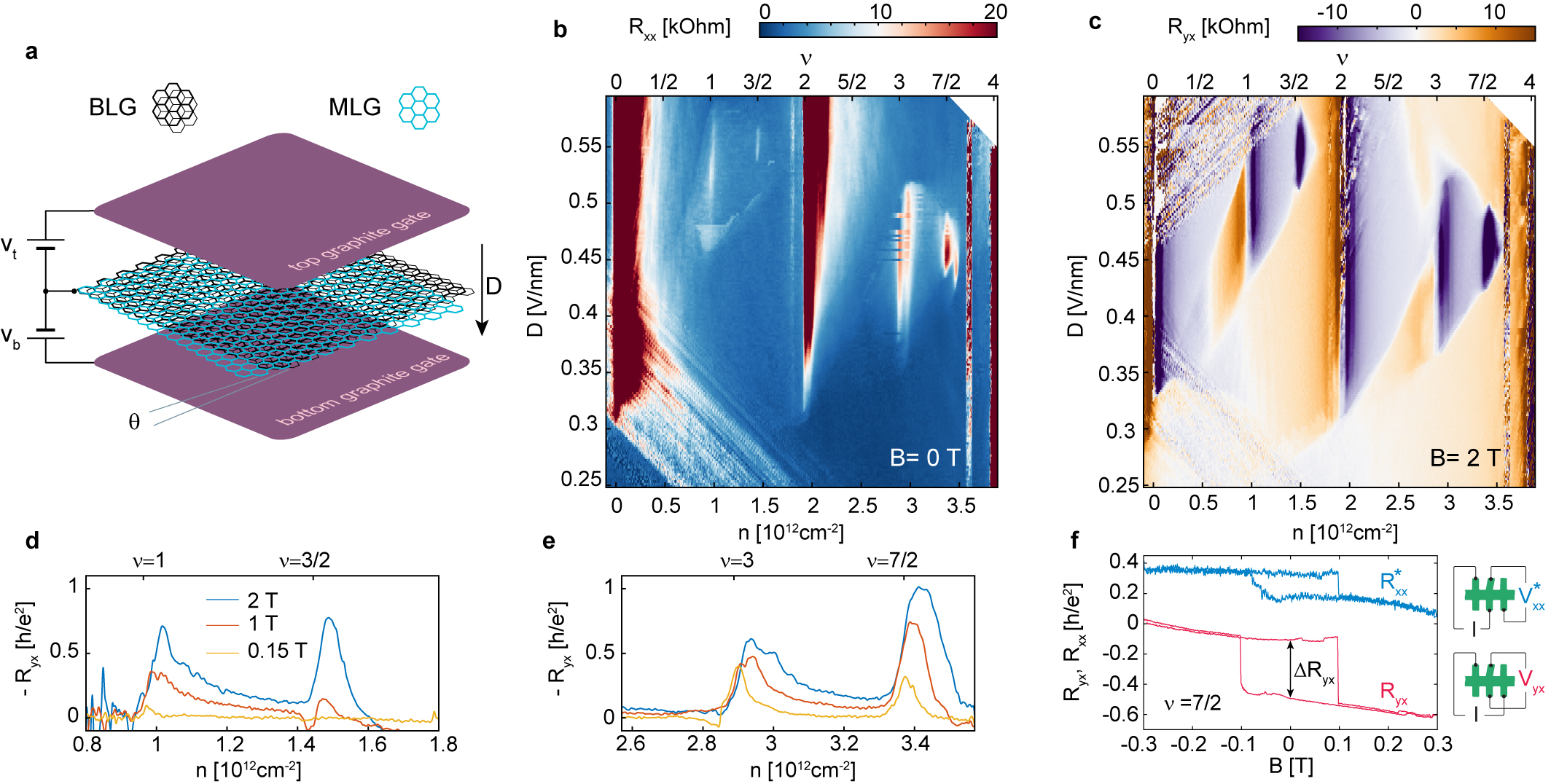
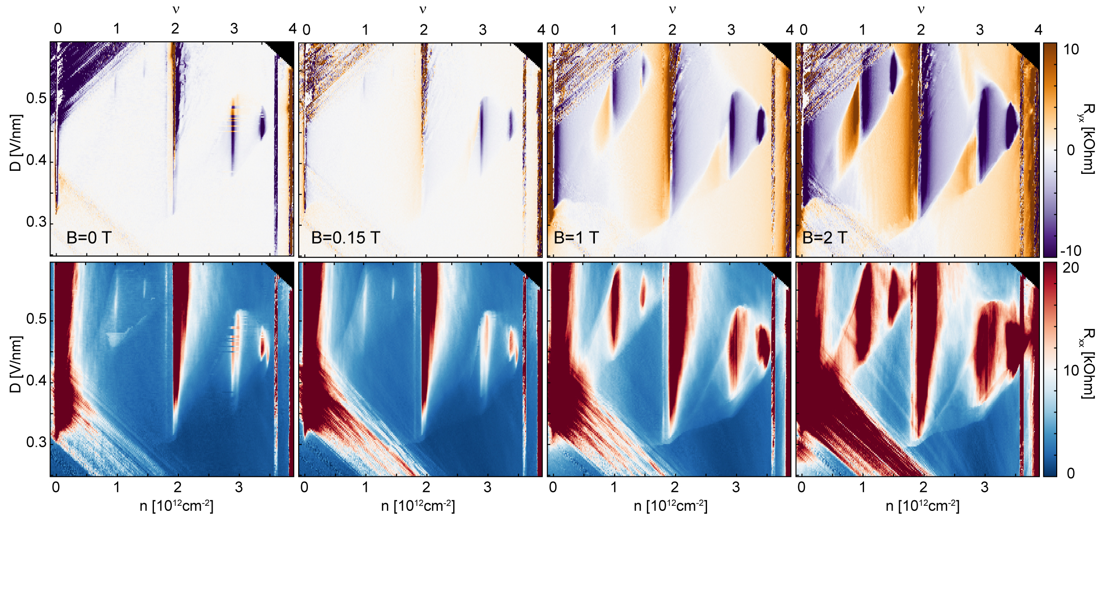
Here, we report the observation of symmetry broken Chern insulator states at half-filling of a Chern 2 band in twisted monolayer-bilayer graphene (tMBG) at zero magnetic field. We study devices in which top and bottom graphite gates enable us to independently control both the total carrier density and the displacement field in the tMBG layer while simultaneously ensuring low charge disorder (see Fig.1a and Methods). Previous studies of this system have demonstrated that the bandwidth and isolation of the low-energy bands are tuned by Polshyn et al. (2020); Chen et al. (2020b); Xu et al. (2021); He et al. (2021), with isolated flat bands realized for twist angles Rademaker et al. (2020); Ma et al. (2021); Park et al. (2020). We focus here on devices with that show correlated insulating states at partial filling of the conduction band for a range of positive displacement fields near V/nm. Figure 1b shows the longitudinal resistance in this regime measured at zero magnetic field and mK in device D2 with twist angle = . Correlated states emerge at all integer fillings of the conduction band as shown in Fig. 1b,c. The state at has zero Chern number, while the states at and 3 are valley-polarized and characterized by Chern number =2, as evidenced by measurements of quantum anomalous Hall effects Polshyn et al. (2020). This finding is consistent with theoretical calculations of the underlying band structure in which valley-projected bands have Rademaker et al. (2020); Ma et al. (2021); Park et al. (2020). Adjacent to the =1 and 3 insulators are regions marked by high contrast in the Hall resistance (Fig. 1c and E2), which we take to correspond to fully flavor (spin and valley) symmetry broken metals.
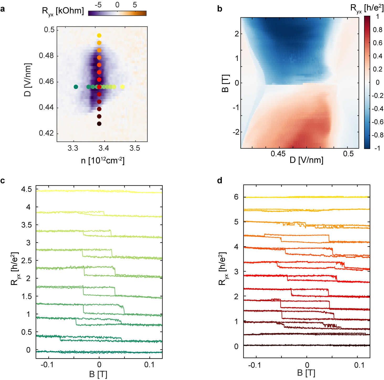
Our primary finding is that correlated states also emerge at several half-integer fillings, manifesting as peaks in the longitudinal resistivity in Figs. 1b at both and . At half-integer fillings we also observe pronounced features in the Hall resistance (see Figs. 1c-e and Fig. E3). The peak at =7/2 approaches at 2 T and persists to low magnetic fields, showing hysteretic behavior with a jump of the Hall resistance of at the coercive field (Fig. 1f). In contrast, at the peak in disappears smoothly as the magnetic field is decreased, though a peak in is still evident at .
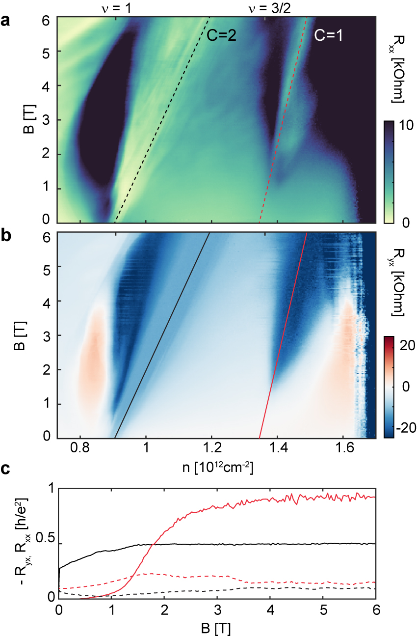
The large Hall effect and commensurate fractional filling suggest that new Chern insulator states emerge at and 7/2, with the former requiring a small magnetic field for stability. To further investigate this hypothesis, we study the magnetic field dependence of these states. Fig. 2 shows and as a function of magnetic field for a range of filling that includes both =1 and 3/2, acquired for a second device (D1, with ). For both states, the density corresponding to the Hall resistivity maximum and longitudinal resistivity minimum evolve with magnetic field following a linear trajectory, as expected from the Streda formula, , which relates the charge carrier density of an incompressible state with applied magnetic field Streda (1982). The Streda formula captures the fact that the degeneracy of the occupied Chern bands is sensitive to the magnetic flux, with a coefficient that encodes the Chern number of the topological gap Xiao et al. (2010). Comparing data from the and Chern insulators suggests Chern numbers of and , respectively. This is confirmed by the magnetic field evolution of the Hall resistance, which approaches the corresponding quantized values for both states for T (Fig. 2c). In both states, the longitudinal resistance is also comparatively small, and shows a minimum as a function of magnetic field and carrier density as expected for a Chern insulator dominated by chiral edge-state conduction. In contrast to the =1 state, which persists down to zero field and exhibits a quantum anomalous Hall effect, the state at =3/2 only emerges in finite magnetic field (see also Fig. E4). Similar behavior is observed in device D2 (Fig. E3).

The magnetic field evolution of a two dimensional gapped state characterized by quantum numbers (, ) is described by the Diophantine equation , where is the number of magnetic flux quanta threading each moiré unit cell Wannier (1978); Streda (1982). From the observed magnetic field dependence of the state we determine . A half-integer value of can be realized only if electronic interactions allow for a fraction of a charge to be bound to a unit cell Oshikawa (2000). This can occur in one of two ways. First, the system may support excitations with fractional charge , as in the fractional quantum Hall effect; however, in the likely realizations of this scenario the Chern number would also be fractional. More conservatively, electron interactions may lead the ground state to spontaneously break the original moiré superlattice symmetries, so that an integer number of electrons are bound to a doubled unit cell; the absence of charge fractionalization however mandates an integer quantized Hall conductivity Kumar et al. (2014). We attribute the state to just such a symmetry broken Chern insulator. This SBCI state splits the spin- and valley- polarized Chern 2 band into two Chern 1 bands, and exists only in the region of the plane near the state, where both spin- and valley- degeneracies are fully broken (see Fig. 1c, E4, E2).
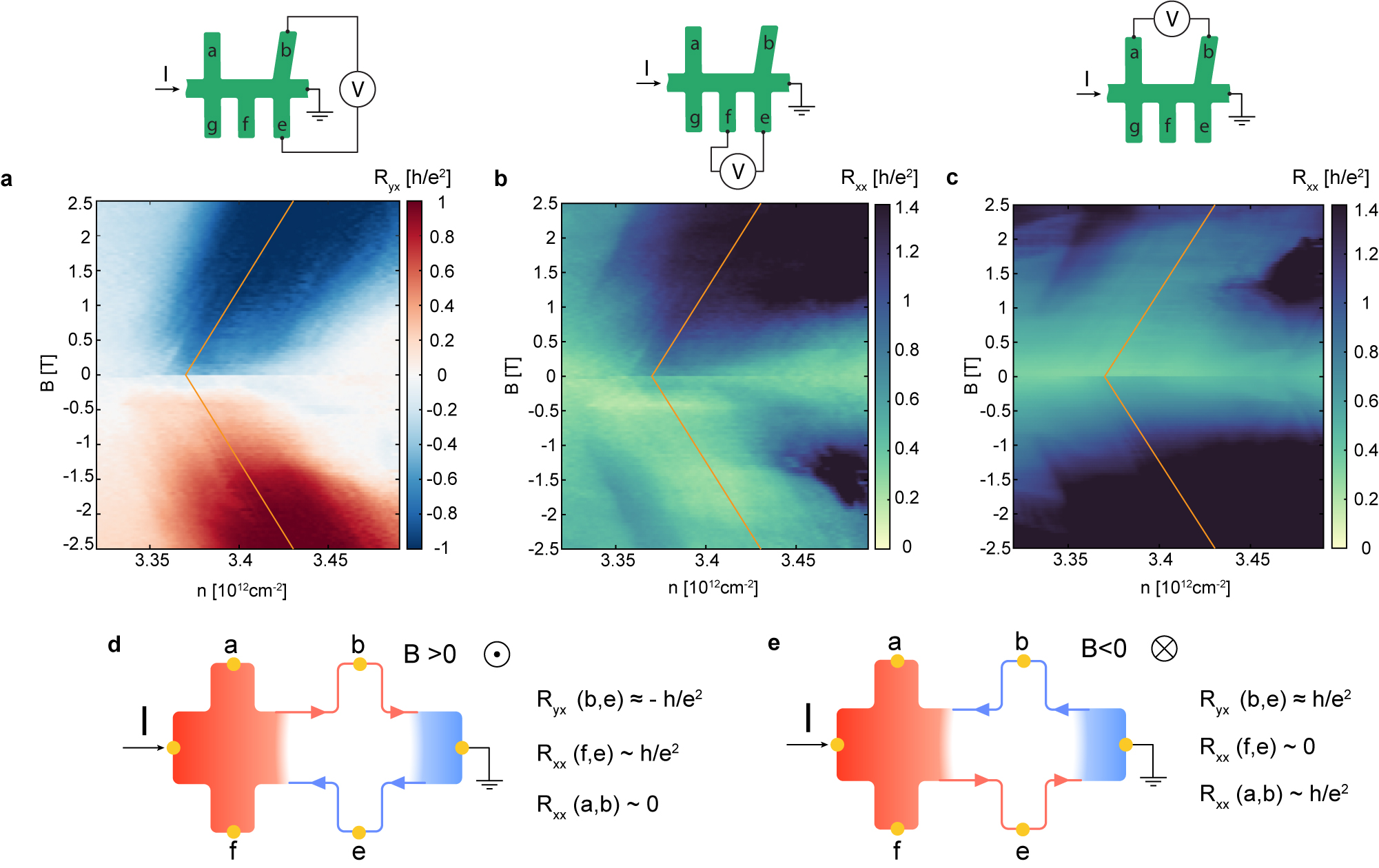
The state observed at shares many features with that at 3/2. It is a symmetry-broken Chern insulating state with =1 and =7/2 as follows from both the Hall conductivity and the - dependence (Fig. 3a). However, in contrast to , the 7/2 state persists all the way down to zero magnetic field and exhibits a large anomalous Hall effect with magnetic hysteresis of and coercive fields of 100 mT (Fig. 3b and Fig. E5). While the Hall conductivity is not perfectly quantized, multiterminal transport measurements strongly suggest that transport is dominated by chiral edge states at , with imperfection of the quantization arising from structural inhomogeneity within the device Uri et al. (2020); Tschirhart et al. (2020) (see Fig. E6). Taking the temperature at which the anomalous Hall resistance at =7/2 disappears as an estimate of the Curie temperature we obtain K (Fig. 3c). This is only about a factor of two smaller than the Curie temperature of QAH states at =1 and 3 Polshyn et al. (2020).
Calculations of the tMBG band structure illuminate the essential features of the moiré minibands that enable SBCI states at fractional filling. In addition to the bandwidth meV, which is significantly smaller than the scale of the Coulomb interaction meV, band structure calculations show a relatively homogeneous distribution of the Berry curvature for the conduction band Park et al. (2020); Rademaker et al. (2020), with similar contributions arising from the neighborhoods of both the and points within the moiré Brillouin zone. Interaction driven doubling of the unit cell at half filling of the band is thus likely to equally partition the evenly distributed Berry curvature, yielding a gap. Such symmetry breaking states constitute a lattice generalisation of quantum Hall ferromagnetism Kumar et al. (2014).
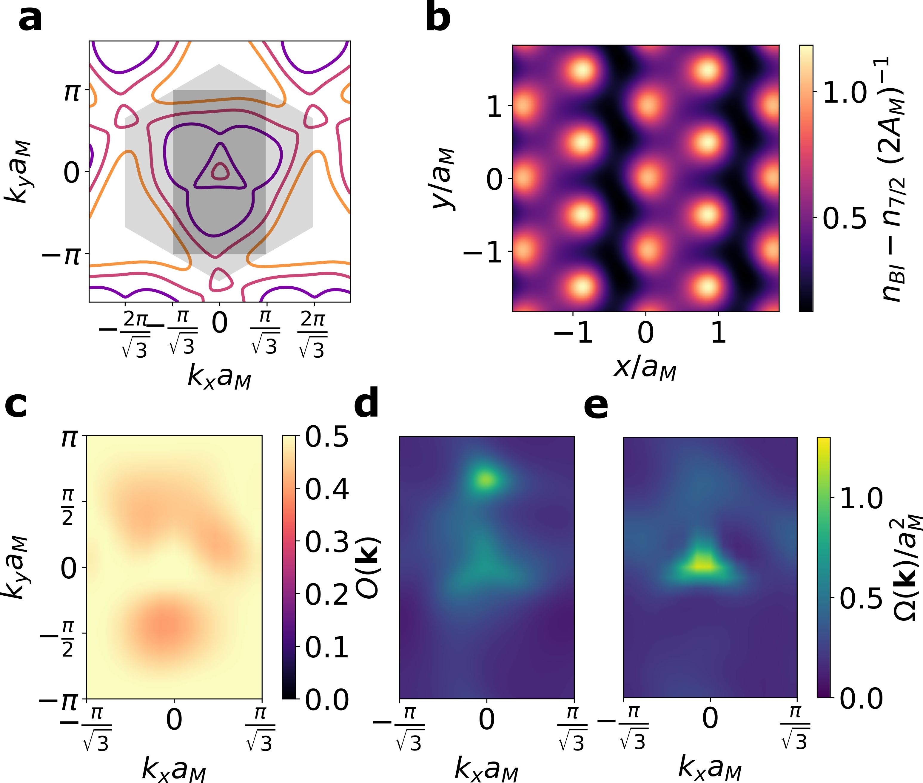
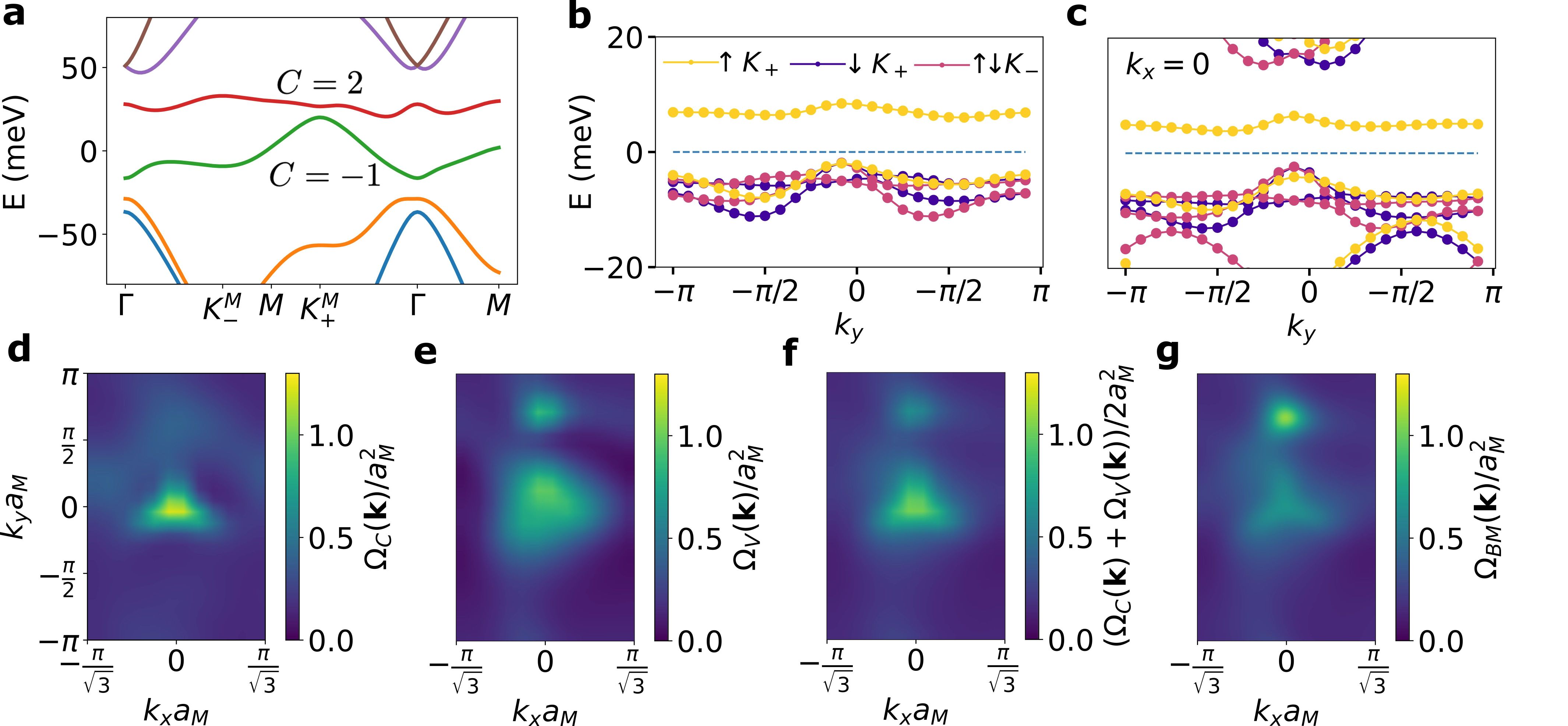
A Hartree-Fock calculation (see Fig. 4), generalized to include translation symmetry breaking that doubles the unit cell, obtains a SBCI ground state for a range of displacement fields around V/nm at filling . The unfilled translation-breaking band is spin and valley polarized and has ; its density and Berry curvature are shown in Fig. 4b,e. The Berry curvature does not have a visible peak at the point, unlike the non-interacting Berry curvature, likely due to interaction-induced mixing with the band below. Finally, the calculated density confirms the stripe order that is inferred from the experimentally-observed half-integer filling, which, in the absence of fractionally quantized Hall resistance, strongly implies unit cell doubling.
The Hartree-Fock state we obtain is very similar to the strong coupling idealized model of sublattice polarization discussed in Kumar et al. (2014). In particular, the translation breaking order parameter for a fully sublattice polarized state on a square lattice is . The analogous order parameter for monolayer-bilayer graphene is plotted in Fig. 4c; it is close to everywhere in the Brillouin zone. This is in sharp contrast to weak coupling translation symmetry breaking, where the order parameter is only significant in regions where the Fermi surface folds on top of itself, such as at the zone boundaries.
Discussion
In their underlying symmetry and topology, the SBCI states we report here belong to the same universality class as those reported previously at high magnetic fields in partially filled Hofstadter bands Wang et al. (2015); Spanton et al. (2018); Saito et al. (2021), where they typically appear at magnetic fields of at least 8 Tesla. Charge density wave physics may also underlie states observed in twisted bilayer graphene at low magnetic fields where is an odd integerYankowitz et al. (2019); Stepanov et al. (2020); Pierce et al. (2021). Charge density wave order can potentially explain these features Kang and Vafek (2020); Pierce et al. (2021) although other mechanisms such as mixing with remote bands Xie and MacDonald (2020) have also been invoked. In comparison, the insulating features described here are more directly interpreted as charge density waves, given that they appear at half-integer filling.
In all cases, interactions gap the Fermi surface by breaking the superlattice symmetry at fractional filling of a Chern band with . SBCI states arise when the Berry curvature is evenly partitioned between occupied and unoccupied states at fractional filling, leading to a topological gap with integer Chern number intermediate between those of adjacent gaps at integer band filling. However, the SBCI states that we report here differ in the key respect that time reversal symmetry is broken spontaneously rather than through the application of a magnetic field. In all previous realizations of correlated topological states at fractional band filling–which includes both SBCIs but also fractionalized states such as fractional quantum Hall effects Tsui et al. (1982) and fractional Chern insulators in Hofstadter bands Spanton et al. (2018)—the underlying Chern band structure is itself a product of the applied magnetic flux. As a result, these systems do not provide a path way to zero magnetic field realizations. In contrast, in twisted monolayer-bilayer graphene the Chern band structure is intrinsic to the moiré miniband structure without applied flux.
In contrast to conventional charge density waves that are well described by a classical order parameter, charge density waves that split a C=2 band have certain special topological features. In these states, topology and charge-density-wave order become entwined. A Chern two band can be understood as analogous to a two-component quantum Hall system in which sub-lattice plays the role of pseudo-spin Kumar et al. (2014), so that dislocations in the charge density-wave order map to non-Abelian fluxes in the pseudo-spin space Barkeshli and Qi (2012). In the SBCI states we find here, this leads to an entwining of charge with topological defects such as lattice dislocations. Directly probing these novel features, and associated phenomena and functionalities, is an exciting and accessible goal for the future. Our results suggest that such states and their attendant defects should be readily accessible in the vast design space of flat band moire heterostructures.
Methods
Device fabrication
Twisted monolayer-bilayer graphene devices were fabricated using a dry transfer method. A PDMS stamp covered with a thin PC (polycarbonate) film was used to subsequently pick up flakes and to create the following van der Waals hetersostructures (from top to bottom): hBN - FLG - hBN - MLG - BLG - hBN -FLG, where hBN is hexagonal boron nitride (usually 30-50 nm thick), FLG - few layer graphene, MLG - monolayer graphene, and BLG - Bernal-stacked bilayer graphene. The vdW heterostructures were further processed using e-beam lithography, etching, and edge contacts deposition (Cr/Pd/Au with thicknesses of 1.5nm/15nm/250nm). Devices D1 and D2 (see fig. E1) in this study are the same as in Ref. Polshyn et al. (2020), which contains more details about the fabrication process.
Device characterization
Top and bottom graphite gates allow us to tune both the total carrier density, , and the electric displacement field, . Here is the applied voltage and is the capacitance per unit area of the top (bottom) gate, is the vacuum permittivity. and are determined by fitting the features of Landau fans for the devices.
A rotational misalignment between MLG and BLG layers by angle produces a moiré superlattice with unit cell area of , where Å. We determine the twist angles of devices by matching the position of the correlated insulating states at integer fillings. In device D2, the positions of features in is fitted well with twist angle = which corresponds to =0.963 . In device D1, we obtain and =0.908 .
Unless specified otherwise, the measurements were performed in a cryogen-free dilution refrigerator at nominal temperature of approximately mK. In case of Fig. E2c, the measurements were done in a wet variable-temperature insert with the sample in helium vapour. Transport measurements were done using lock-in amplifiers (SRS), voltage pre-amplifiers (SRS), and a current amplifier (DL Instruments) with excitation currents of 1-5 nA at 17.77 Hz.
In device D2, unless indicated otherwise, the four point resistance measurements of and were done by measuring voltage drop across the pairs of contacts labeled as (b, e) and (f, e) respectively as indicated in Fig. E1b.
Hartree-Fock simulations
Hartree-Fock simulations were performed with the non-interacting Hamiltonian identical to the Hamiltonian described in the supplement of Ref. Polshyn et al. (2020). We used the parameters , V/nm, in all plots. We allowed for translation symmetry breaking that doubled the unit cell; translation breaking states that more than doubled the unit cell or broke out of plane spin rotations were excluded. More details and results are shown in the supplemental material.
acknowledgments
The authors are grateful to Jihang Zhu for fruitful discussions. AFY acknowledges support of the Office of Naval Research under award N00014-20-1-2609, and the Gordon and Betty Moore Foundation under award GBMF9471. MPZ acknowledges support of the ARO under MURI W911NF-16-1-0361. KW and TT acknowledge support from the Elemental Strategy Initiative conducted by the MEXT, Japan, Grant Number JPMXP0112101001, JSPS KAKENHI Grant Numbers JP20H00354 and the CREST(JPMJCR15F3), JST. AV was supported by a Simons Investigator Award. P.L. was supported by the Department of Defense (DoD) through the National Defense Science & Engineering Graduate Fellowship (NDSEG) Program.
Author contributions
HP, MAK, and YZ fabricated the devices. HP performed the measurements, advised by AFY. KW and TT grew the hexagonal boron nitride crystals. TS, PL, MPZ, and AV contributed to the theoretical interpretation and performed the Hartree-Fock calculations. HP, PL, and AFY wrote the manuscript with input from all other authors.
Competing interests
The authors declare no competing interests.
Data availability
The data that support the plots within this paper and other findings of this study are available from the corresponding author upon reasonable request.
References
- Tsui et al. (1982) D. C. Tsui, H. L. Stormer, and A. C. Gossard, Phys. Rev. Lett. 48, 1559 (1982).
- Wang et al. (2015) L. Wang, Y. Gao, B. Wen, Z. Han, T. Taniguchi, K. Watanabe, M. Koshino, J. Hone, and C. R. Dean, Science 350, 1231 (2015).
- Spanton et al. (2018) E. M. Spanton, A. A. Zibrov, H. Zhou, T. Taniguchi, K. Watanabe, M. P. Zaletel, and A. F. Young, Science 360, 62 (2018).
- Chen et al. (2020a) G. Chen, A. L. Sharpe, E. J. Fox, Y.-H. Zhang, S. Wang, L. Jiang, B. Lyu, H. Li, K. Watanabe, T. Taniguchi, Z. Shi, T. Senthil, D. Goldhaber-Gordon, Y. Zhang, and F. Wang, Nature 579, 56 (2020a).
- Serlin et al. (2020) M. Serlin, C. L. Tschirhart, H. Polshyn, Y. Zhang, J. Zhu, K. Watanabe, T. Taniguchi, L. Balents, and A. F. Young, Science 367, 900 (2020).
- Stepanov et al. (2020) P. Stepanov, M. Xie, T. Taniguchi, K. Watanabe, X. Lu, A. H. MacDonald, B. A. Bernevig, and D. K. Efetov, arXiv:2012.15126 [cond-mat] (2020).
- Polshyn et al. (2020) H. Polshyn, J. Zhu, M. A. Kumar, Y. Zhang, F. Yang, C. L. Tschirhart, M. Serlin, K. Watanabe, T. Taniguchi, A. H. MacDonald, and A. F. Young, Nature 588, 66 (2020).
- Zhang et al. (2019) Y.-H. Zhang, D. Mao, Y. Cao, P. Jarillo-Herrero, and T. Senthil, Physical Review B 99, 075127 (2019).
- Ledwith et al. (2020) P. J. Ledwith, G. Tarnopolsky, E. Khalaf, and A. Vishwanath, Physical Review Research 2, 023237 (2020).
- Repellin and Senthil (2020) C. Repellin and T. Senthil, Physical Review Research 2, 023238 (2020).
- Abouelkomsan et al. (2020) A. Abouelkomsan, Z. Liu, and E. J. Bergholtz, Physical Review Letters 124, 106803 (2020).
- Wilhelm et al. (2021) P. Wilhelm, T. C. Lang, and A. M. Läuchli, Physical Review B 103, 125406 (2021).
- Chen et al. (2020b) S. Chen, M. He, Y.-H. Zhang, V. Hsieh, Z. Fei, K. Watanabe, T. Taniguchi, D. H. Cobden, X. Xu, C. R. Dean, and M. Yankowitz, Nature Physics , 1 (2020b).
- Xu et al. (2021) S. Xu, M. M. Al Ezzi, N. Balakrishnan, A. Garcia-Ruiz, B. Tsim, C. Mullan, J. Barrier, N. Xin, B. A. Piot, T. Taniguchi, K. Watanabe, A. Carvalho, A. Mishchenko, A. K. Geim, V. I. Fal’ko, S. Adam, A. H. C. Neto, K. S. Novoselov, and Y. Shi, Nature Physics , 1 (2021).
- He et al. (2021) M. He, Y.-H. Zhang, Y. Li, Z. Fei, K. Watanabe, T. Taniguchi, X. Xu, and M. Yankowitz, arXiv:2101.04063 [cond-mat] (2021).
- Kumar et al. (2014) A. Kumar, R. Roy, and S. L. Sondhi, Physical Review B 90, 245106 (2014).
- Kitaev (2009) A. Kitaev, AIP Conf. Proc. 1134, 22 (2009).
- Haldane (1988) F. D. M. Haldane, Phys. Rev. Lett. 61, 2015 (1988).
- Chang et al. (2013) C.-Z. Chang, J. Zhang, X. Feng, J. Shen, Z. Zhang, M. Guo, K. Li, Y. Ou, P. Wei, L.-L. Wang, Z.-Q. Ji, Y. Feng, S. Ji, X. Chen, J. Jia, X. Dai, Z. Fang, S.-C. Zhang, K. He, Y. Wang, L. Lu, X.-C. Ma, and Q.-K. Xue, Science 340, 167 (2013).
- Deng et al. (2020) Y. Deng, Y. Yu, M. Z. Shi, Z. Guo, Z. Xu, J. Wang, X. H. Chen, and Y. Zhang, Science (2020), 10.1126/science.aax8156.
- Dean et al. (2020) C. Dean, P. Kim, J. I. A. Li, and A. Young, in Fractional Quantum Hall Effects: New Developments (World Scientific, Singapore, 2020) pp. 317–375.
- Thouless et al. (1982) D. J. Thouless, M. Kohmoto, M. P. Nightingale, and M. den Nijs, Phys. Rev. Lett. 49 (1982).
- Sharpe et al. (2019) A. L. Sharpe, E. J. Fox, A. W. Barnard, J. Finney, K. Watanabe, T. Taniguchi, M. A. Kastner, and D. Goldhaber-Gordon, Science 365, 605 (2019).
- Chen et al. (2020c) G. Chen, A. L. Sharpe, E. J. Fox, S. Wang, B. Lyu, L. Jiang, H. Li, K. Watanabe, T. Taniguchi, M. F. Crommie, M. A. Kastner, Z. Shi, D. Goldhaber-Gordon, Y. Zhang, and F. Wang, arXiv:2012.10075 [cond-mat] (2020c).
- Regan et al. (2020) E. C. Regan, D. Wang, C. Jin, M. I. Bakti Utama, B. Gao, X. Wei, S. Zhao, W. Zhao, Z. Zhang, K. Yumigeta, M. Blei, J. D. Carlström, K. Watanabe, T. Taniguchi, S. Tongay, M. Crommie, A. Zettl, and F. Wang, Nature 579, 359 (2020).
- Xu et al. (2020) Y. Xu, S. Liu, D. A. Rhodes, K. Watanabe, T. Taniguchi, J. Hone, V. Elser, K. F. Mak, and J. Shan, Nature 587, 214 (2020).
- Jin et al. (2020) C. Jin, Z. Tao, T. Li, Y. Xu, Y. Tang, J. Zhu, S. Liu, K. Watanabe, T. Taniguchi, J. C. Hone, L. Fu, J. Shan, and K. F. Mak, arXiv:2007.12068 [cond-mat] (2020).
- Huang et al. (2020) X. Huang, T. Wang, S. Miao, C. Wang, Z. Li, Z. Lian, T. Taniguchi, K. Watanabe, S. Okamoto, D. Xiao, S.-F. Shi, and Y.-T. Cui, arXiv:2007.11155 [cond-mat] (2020).
- Rademaker et al. (2020) L. Rademaker, I. V. Protopopov, and D. A. Abanin, Phys. Rev. Research 2, 033150 (2020).
- Ma et al. (2021) Z. Ma, S. Li, Y.-W. Zheng, M.-M. Xiao, H. Jiang, J.-H. Gao, and X. Xie, Science Bulletin 66, 18 (2021).
- Park et al. (2020) Y. Park, B. L. Chittari, and J. Jung, Phys. Rev. B 102, 035411 (2020).
- Streda (1982) P. Streda, J. Phys. C: Solid State Phys. 15 (1982).
- Xiao et al. (2010) D. Xiao, M.-C. Chang, and Q. Niu, Reviews of Modern Physics 82, 1959 (2010).
- Wannier (1978) G. H. Wannier, phys. stat. sol. (b) 88, 757 (1978).
- Oshikawa (2000) M. Oshikawa, Physical Review Letters 84, 1535 (2000).
- Uri et al. (2020) A. Uri, S. Grover, Y. Cao, J. A. Crosse, K. Bagani, D. Rodan-Legrain, Y. Myasoedov, K. Watanabe, T. Taniguchi, P. Moon, et al., Nature 581, 47 (2020).
- Tschirhart et al. (2020) C. L. Tschirhart, M. Serlin, H. Polshyn, A. Shragai, Z. Xia, J. Zhu, Y. Zhang, K. Watanabe, T. Taniguchi, M. E. Huber, and A. F. Young, arXiv:2006.08053 [cond-mat] (2020).
- Saito et al. (2021) Y. Saito, J. Ge, L. Rademaker, K. Watanabe, T. Taniguchi, D. A. Abanin, and A. F. Young, Nature Physics , 1 (2021).
- Yankowitz et al. (2019) M. Yankowitz, S. Chen, H. Polshyn, Y. Zhang, K. Watanabe, T. Taniguchi, D. Graf, A. F. Young, and C. R. Dean, Science 363, 1059 (2019).
- Pierce et al. (2021) A. T. Pierce, Y. Xie, J. M. Park, E. Khalaf, S. H. Lee, Y. Cao, D. E. Parker, P. R. Forrester, S. Chen, K. Watanabe, T. Taniguchi, A. Vishwanath, P. Jarillo-Herrero, and A. Yacoby, arXiv:2101.04123 [cond-mat] (2021).
- Kang and Vafek (2020) J. Kang and O. Vafek, Physical Review B 102, 035161 (2020).
- Xie and MacDonald (2020) M. Xie and A. H. MacDonald, Physical Review Letters 124, 097601 (2020).
- Barkeshli and Qi (2012) M. Barkeshli and X.-L. Qi, Physical Review X 2, 031013 (2012).
- Polshyn et al. (2019) H. Polshyn, M. Yankowitz, S. Chen, Y. Zhang, K. Watanabe, T. Taniguchi, C. R. Dean, and A. F. Young, Nature Physics 15, 1011 (2019).
- Soejima et al. (2020) T. Soejima, D. E. Parker, N. Bultinck, J. Hauschild, and M. P. Zaletel, Phys. Rev. B 102, 205111 (2020).
- Fukui et al. (2005) T. Fukui, Y. Hatsugai, and H. Suzuki, Journal of the Physical Society of Japan 74, 1674 (2005).
- Marzari et al. (2012) N. Marzari, A. A. Mostofi, J. R. Yates, I. Souza, and D. Vanderbilt, Rev. Mod. Phys. 84, 1419 (2012).
- Qi (2011) X.-L. Qi, Phys. Rev. Lett. 107, 126803 (2011).
- Marzari and Vanderbilt (1997) N. Marzari and D. Vanderbilt, Phys. Rev. B 56, 12847 (1997).


I Supplementary Information
The non-interacting band structure was obtained from the Hamiltonian identical to those described in Polshyn et al. (2019). We obtain the renormalized non-interacting band structure using subtraction method described in the Appendix of Soejima et al. (2020), and perform Hartree-Fock calculation with respect to double gate screened Coulomb potential with relative permittivity and gate distance nm.
Hartree-Fock simulations were performed for a range of parameters close to the filling . We allowed for translation symmetry breaking states that doubled the unit cell by demanding that translations along the axis are preserved, and that other translations are preserved at order two. This leads to the rectangular Brillouin zone shown in Figure 4a. While there are two other ways to double the unit cell, they are related to this one by symmetry. We do not allow for spin rotations about the out of plane axis to be broken; while this still allows for spin polarized states it excludes some spin density wave states. We confirm the Chern number of the Hartree-Fock ground state via the plaquette method Fukui et al. (2005) and via winding of Wannier polarization, as described below.
A crude sweep across different displacement fields found an SBCI ground state close to V/nm. This state has , as it leaves a single band unfilled, and it breaks translation symmetry with close to maximal magnitude across the entire Brillouin zone as shown by the plot of the translation breaking order parameter in Figure 4c. We chose
| (1) |
where and label the valley and spin that are not fully filled and and index the non-interacting bands; most of the contribution is from the term where and both index the band as expected. The translation breaking wavevector is .
We show more details about the Hartree-Fock ground state at V/nm in Figures S1 and S2. In figure S1a we plot the non-interacting band structure. The flat band is our band of interest; note that it comes close to touching the band below it at the point. Hartree-Fock band structures are shown in Figure S1b,c with and without remote bands included respectively; The band in graphene valley with spin up splits into the two yellow bands shown after translation breaking, one of which is occupied. The other six bands, with spin down and/or graphene valley , are all occupied giving a total filling of (note that the bands in valley are spin degenerate since spin rotations in that valley remain unbroken).
Adding remote bands does not change the state dramatically, although the Berry curvature at the point diminishes likely due to mixing with the band below due to the near gap closing point. We may see this by comparing the average of the Berry curvature of the two Hartree-Fock bands with the average of the folded Berry curvature of the non interacting bands. While these averages are and should be identical when no remote bands are included, the Berry curvature at the point is diminished relative to the non-interacting case when remote bands are included.
One way to view the band splitting into two bands is through hybrid Wannier functions. While there are no fully localized Wannier functions for Chern bands, we may localize the states along the direction while keeping the state delocalized along and labeled by Marzari et al. (2012); Qi (2011). We obtained maximally localized hybrid wannier functions and their polarization for band following the algorithm in Marzari and Vanderbilt (1997). In this basis the Chern number manifests itself through the winding of the polarization: as winds around the Brillouin zone the position of the Wannier function shifts by unit cells in the direction as shown in Figure S2a. Furthermore, when we double the unit cell we obtain two branches of Wannier functions that each wind once, see Figure S2b, and therefore describe two bands Barkeshli and Qi (2012). The “forgotten” translation symmetry exchanges these two bands. We find that the Hartee Fock SBCI state essentially picks one of these Chern bands to fill and leaves the other unfilled; the polarization is shown in Figure S2c and it is almost maximal everywhere in the Brillouin zone. It seems to look very similar to the plot of the translation breaking order parameter in Figure 4c as well.
