Andreev interference in the surface accumulation layer of half-shell InAsSb/Al hybrid nanowires
Abstract
Understanding the spatial distribution of charge carriers in III-V nanowires proximity coupled to superconductors is important for the design and interpretation of experiments based on hybrid quantum devices. In this letter, the gate-dependent surface accumulation layer of InAsSb/Al nanowires was studied by means of Andreev interference in a parallel magnetic field. Both uniform hybrid nanowires and devices featuring a short Josephson junction fabricated by shadow lithography, exhibited periodic modulation of the switching current. The period corresponds to a flux quantum through the nanowire diameter and is consistent with Andreev bound states occupying a cylindrical surface accumulation layer. The spatial distribution was tunable by a gate potential as expected from electrostatic models.
Semiconductor nanowires (NWs) with superconducting electrodes provide a flexible experimental platform for studies of mesoscopic superconductivity. Experiments have demonstrated tunableDoh et al. (2005) and reversibleVan Dam et al. (2006) supercurrents, Cooper pair splittingHofstetter et al. (2009), electron pumping Giazotto et al. (2011), gate-tunable superconducting qubitsLarsen et al. (2015), and have provided a detailed understanding of Andreev bounds states (ABS)Prada et al. (2020) and topological Majorana zero modesOreg et al. (2010); Lutchyn et al. (2010); Mourik et al. (2012); Albrecht et al. (2016). The performance of NW hybrid devices is strongly affected by crystal defectsKretinin et al. (2010); Schroer and Petta (2010), interface disorderKrogstrup et al. (2015), and surface scatteringLynall et al. (2018) and the experimental progress has gone hand-in-hand with developments of materials and methods for device fabrication to minimize sources of disorder. High-mobility semiconductor NWs can now be grown into complex geometriesDalacu et al. (2013); Gazibegovic et al. (2017) with a negligible amount of crystal defects, and the development of in-situ growth of epitaxial semiconductor/superconductor hybridsKrogstrup et al. (2015) enables reproducible, uniform contacting and improved character of induced superconductivityChang et al. (2015). Finally, in-situ shadow patterning methods have been developed to reduce post growth processingCarrad et al. (2020); Khan et al. (2020); Gazibegovic et al. (2017); Krizek et al. (2017); Heedt et al. (2020) and thus significantly reduce random scattering from surface adsorbents, and improve reproducibility and electrostatic stability. With minimal disorder and extrinsic random scattering, intrinsic properties such as the non-uniform carrier distribution can be dominating. In low band gap III-V-compounds such as InAs or InSb the surface Fermi level is pinned in the conduction bandOlsson et al. (1996) and for the NW geometry, the expectation is a cylindrical electron accumulation layer as also found in Schrödinger-Poisson modelingWinkler et al. (2019); Mikkelsen et al. (2018); Antipov et al. (2018). Early Kelvin probe microscopyHalpern et al. (2012) and studies of the scaling of room-temperature resistance with the diameterDayeh et al. (2009); Scheffler et al. (2009) is consistent with this scenario, however, clear confirmation in quantum devices operating at low temperature is lacking.
Quantum interference in Josephson devices in a magnetic field provides a sensitive probe of the spatial electron distribution and has been used to study the emergence of edge states in topological insulatorsHart et al. (2014). Here we measured the magnetoconductance of high mobility InAsSb NWs with epitaxial aluminum grown on two facets of the hexagonal nanowire. We consider both devices with a continuous Al and devices where a Josephson junction (JJ) is realized by in-situ shadow lithographyKhan et al. (2020). Interference patterns periodically modulated by the flux through the NW cross-section are reproducibly found over all six devices and confirm the presence of a proximitized cylindrical accumulation layer at the NW surface. We show that this property is not limited to the JJ geometry but relevant also in uniform hybrid NWs and in both classes of devices, electrostatic gating tunes the density and spatial distribution of the carriers and the cylindrical geometry is lost at large negative gate potentials consistent with electrostatic modelingWinkler et al. (2019); Mikkelsen et al. (2018); Antipov et al. (2018). The results are important for the interpretation result obtained from NW quantum devices and we discuss the relation to the Little-Parks effect observed in full shell hybrid NWs Vaitiekenas et al. (2020).
.1 Experimental details
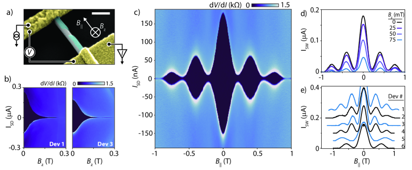
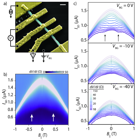
Devices were fabricated using InAsSb NW grown from (111)B facets etched into a (100) InAs substrateKhan et al. (2020); Gazibegovic et al. (2017). The InAsSb ternary alloy was chosen as a compromise between the high mobility and low effective mass of InSb and the higher chemical robustness of InAsKhan et al. (2020); Sestoft et al. (2018). The NWs feature a hexagonal cross section and following semiconductor growth, of epitaxial aluminum was grown on two of the 6 facets without breaking the reactor vacuum.Krogstrup et al. (2015); Khan et al. (2020) For JJ devices, wide gaps in the Al were realized in-situ by shadowing Al growth by adjacent NWsKrizek et al. (2017); Gazibegovic et al. (2017); Khan et al. (2020). The obviation of subsequent fabrication steps and etching leads to low disorder and electrostatically stable devicesCarrad et al. (2020). For measurements, individual NWs were transferred to standard Si/SiOx substrates where the doped Si acts as back-gate isolated from the NWs by of . Ti/Au Ohmic contacts were defined by standard lithography and Figs. 1a and 4a show scanning electron micrographs of a finished device with shadow junctions and continuous Al, respectively. While transferring NWs to the device substrate, the orientation of the Al facets to the substrate plane was not controlled, and devices with a significantly reduced gate-response were attributed to hybrids with Al facing the back-gate. Such samples were not included in further measurements. Measurements were performed in a dilution refrigerator with a base temperature of and equipped with a 3D vector magnet. For each device the orientation of the nanowire axis was determined with an accuracy of by measuring the anisotropy of the critical magnetic field and this allowed application of magnetic field along the axis of the nanowires. For uniform InAsSb/Al devices the differential resistance was measured in a four-terminal configuration (Fig. 4a) while JJ segments were measured in a pseudo four-terminal configuration and contact resistances, identified as the baseline resistance in the superconducting state, were subsequently subtracted. In total, nine devices were measured; six with JJs (Dev. 1-6) and three without (Dev. 7-9). In each category all devices showed qualitatively consistent behavior and in the following, results from one representative device of each type is presented; results from remaining devices are included in the Supporting Information.
.2 Results
We consider first the JJ devices which isolates the contribution of the semiconductor and then subsequently discuss the situation in the uniform hybrid nanowires with continious Al. Figure 1b shows the differential resistance of JJ Devices 1 and 3 as a function of the perpendicular out-of-plane magnetic field sweeping from negative to positive. A zero-resistance superconducting region is observed at low currents and the switching current where the device switches to a finite resistance state decreases monotonously with and at superconductivity is completely suppressed consistent with previous measurements of epitaxial hybrid nanowires in a perpendicular field Chang et al. (2015); Heedt et al. (2020). A strikingly different behavior is observed in the corresponding measurement performed with the field applied parallel to the NW (Fig. 4c). Pronounced oscillations of the switching current appear with a period of . The amplitude decreases towards higher as superconductivity is gradually suppressed but due to the thin Al, the critical magnetic field is larger in the parallel direction and although it is strongly suppressed at the minima of the oscillations, the switching current remains finite up to the highest applied magnetic field of 1 T. In Fig. 1d the dependence of the switching current on has been extracted from measurements similar to Fig. 1c repeated for various . The oscillation amplitude decreases with following the envelope in Fig. 1b, however the period and qualitative shape of the modulation is independent of . The experiment was repeated for a number of devices and Fig. 1e shows the switching current for 6 JJ devices extracted from full maps like Fig. 1c; (see SI Fig. S4). All devices exhibit qualitatively similar periodic modulation with a small variation in the period between the different devices as discussed below.
Gate dependence of interference pattern
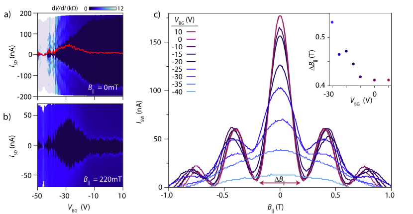
The modulation in Fig. 1c is the main experimental result of this work and we now consider the effect of changing the overall carrier density in the junction using the back-gate. Figure 2a shows the differential resistance vs. and for . The switching current appears as the first contour with a non-zero and decreases from to zero upon lowering from to because the -type semiconductor is depleted of carriersDoh et al. (2005); Khan et al. (2020). In Fig. 2c, the dependence of on is shown for different (see SI Fig. S6 for full maps). The periodic nature of -modulations is not affected by . However as the junction is depleted the peak amplitude decreases and the period of the modulation increases slightly as emphasized in the inset, which shows the dependence of the difference between the two first minima as indicated on the Fig. 2c (SI Fig. S11). Only close to pinch-off does the modulation disappear.
At the minima of the oscillations, the switching current increases with decreasing despite the increasing NW resistance. This unusual behavior is emphasized in Fig. 2b which shows a measurement similar to Fig. 2a, however, measured with close to the first minimum. At a highly suppressed is observed. Upon decreasing , remains constant until from where on first increases as the interference pattern is gradually lost, to a maximum of at after which it re-traces the decrease observed for . For comparison, this unconventional for is extracted and shown in Fig. 2(a) (red trace).

Fraunhofer interference of supercurrents is a typical source of -modulations in JJs due to field induced spatial dependence of the superconducting phase in the leads. Therefore, two different measurements were performed to investigate whether the observed effect is specific to the JJ geometry. First, by operating the JJ-devices with close to pinch-off, measurements at finite voltage bias effectively performs spectroscopy of the density of states in the leads. Secondly, direct measurements of the effect of on uniformely coated nanowires without JJ were performed.
Spectroscopy at finite bias
Figure 3a shows as a function of the DC bias voltage and . The sweeping direction is from positive to negative. Heavy filtering of the DC lines makes the measurement effectively current-biased at low and a smooth re-trapping transition compared to the abrupt switching-current results in the asymmetry of the low-bias part of the figure. A series of symmetric features are observed (arrows) at voltages which do not depend on the junction transparency (which decreases with ) and are therefore associated with properties of the leads. The features are also emphasized in panel (b) showing a trace extracted for fixed and follow the expected harmonic sub gap structure due to multiple Andreev reflections (MAR) as commonly observed in nanowire JJs Doh et al. (2005); Ridderbos et al. (2019); Shailos et al. (2007); Nilsson et al. (2012). The extracted gap is consistent with the expected gap of the Al hybrids Chang et al. (2015). In addition to the MAR features, spectroscopic measurements also probe sub-gap states in the leadsHeedt et al. (2020) and Fig. 3c shows a measurement of the spectrum as a function of for a fixed . A rich spectrum emerges at finite which is originating from the peak and is following a pattern modulating similar to the switching current in Figs. 1-2. This demonstrates that the observed interference is not exclusively a junction property. We attribute the fainter features in Fig. 3c which coincide at with and and smoothly closes around to the sub-gap-structure reflecting the slow dependence of on .
Uniform nanowires
As a final confirmation we consider the measurements of devices with continuous Al (Fig. 4a). Due to the higher charge carrier density, transport is dominated by the Al, however, as the metal shell is not susceptible to gating, the contribution of the semiconductor can be identified by the dependence on . Figure 4b shows the dependence of four terminal on and . The switching current appears as a pronounced increase in the resistance (white contour), and the finite resistance observed also for is attributed to phase slips and is commonly observed in 1D superconductor NWs Li et al. (2011); Golubev and Zaikin (2018); Rogachev et al. (2005); Sahu et al. (2009). The zero field and the critical magnetic field (extrapolated from Fig. 4b) is similar but slightly lower than previous studies of epitaxial hybrid nanowiresMeservey and Tedrow (1971); Krogstrup et al. (2015), which might be due to a grainy Al. The switching current decreases with and exhibits kinks at (arrows) which are more clearly seen in Fig. 4c which shows constant-resistance contours extracted from Fig. 4c and corresponding measurements at three different . The zero field switching current decreases from for to for , and the kinks in the contours disappear upon lowering . The gate dependence is consistent with a supercurrent carried partly by the Al shell and partly by the semiconductor. Here, the latter contribution decreases as the semiconductor is depleted at low and since the kinks at finite also disappear these are related to the presence of the semiconductor. The qualitative resemblance of these results with the JJ measurements serves as an additional indication that the interference is not a JJ effect but a property of the hybrid nanowire materials.
I Discussion
The regular modulation observed here – i.e. fringes with regular period in that behave monotonically with – contrasts previous reports on supercurrent interference in NW devices, which generally feature aperiodic patterns in field and gate voltage due to random interferenceZuo et al. (2017); Gharavi and Baugh (2015); Gharavi et al. (2017). Depending on the current distribution, conventional Fraunhofer interference can lead to periodic oscillationsHart et al. (2014); Paajaste et al. (2015), however, such a mechanism is inconsistent with the observed modulation in the JJ leads (Fig. 3) and in the junctionless devices (Fig. 4). A key feature of the observed behaviour is that only the field component parallel to the NW modulates , suggesting a relation to states acquiring a phase while encircling the NW surface. This is also consistent with the period of the oscillations, which we associate with the field required to add a flux quantum through a typical cross-sectional area. Assuming a cylindrical geometry we get , where is the effective diameter, is the Planck constant and the electron charge. For devices 1-4, corresponds to a diameter nm, and for devices 5 and 6, the corresponding flux diameter was nm. The physical nanowire diameters, , were independently estimated from SEM micrographs (Supporting Fig. S1) as nm and nm for devices 1-4 and 5-6, respectively. Given that numerical and theoretical estimates have shown the surface accumulation layer thickness to be 15-20 nm, the period is consistent with electron interference in the accumulation layer. A main result of the current work is therefore that transport in the InAsSb NW devices is dominated by carriers occupying a surface accumulation layer.
We now consider the physical mechanism leading to the behaviour. In an Aharonov-Bohm (AB) ring between two superconductors with phase difference , Andreev bound states (ABS) form with energyDolcini and Giazotto (2007)
| (1) |
Here, is the AB phase, is the flux penetrating the ring, and is the flux-dependent transmission. Extending this concept to the situation in the JJ leads – which consist of a hybrid NW partially covered by the Al film – ABS form around the NW circumference due to Andreev reflection from the single superconductor, corresponding to . This situation is similar to reflectionless tunnelingvan Wees et al. (1992), albeit with a fixed area for phase accumulation here. The result is a periodic modulation of the semiconductor/superconductor coupling, as previously observed for nanoscale core/shell cylindersGül et al. (2014). The ABS energies are modulated by and are minimal at . For a diameter of 80 nm, the first minima would be expected to occur at ,Zhou et al. (1998); le Sueur et al. (2008) consistent with the spectroscopic measurements in Fig. 3. The modulation of the in the uniform hybrid nanowires in Fig. 4 can thereby be accounted for by the periodic modulation of the ABS energies, combined with a reduction of the InAsSb/Al coupling.
In the case of the JJ devices, for , the phase difference across the junction, , varies with to ensure a dissipation-less supercurrent . Therefore, an AB-phase only acts as an offset, which can be compensated by and thus not result in modulations. Instead, the observed oscillations in the JJs are a consequence of the transmission , which oscillates due to the conventional AB effect Aharonov and Bohm (1959). We note that resistance oscillations were not clearly resolved in the normal state for which we attribute to a shorter phase coherence length at elevated temperature or the dominating contribution of channels with high transmission in the superconducting stateMurani et al. (2017).
The number of transverse modes and their degeneracies in the hybrid nanowires, as well as the gatability and coupling to magnetic fields, are important for interpreting results and the prospects of realizing theoretical proposals for topological devicesOreg et al. (2010); Lutchyn et al. (2010); Vaitiekenas et al. (2020). The gate-dependence of the interference pattern in Fig. 4 probes the changes of the density profile. Due to screening by the grounded Al half shell, the gate acts more strongly on the JJ segment than below the superconductor, and affects most strongly the part of this segment facing the back gate. At the interference pattern and significant suppression of at shows that electrons occupy the cylindrical accumulation layer near the surface of the NW. Upon decreasing the resistance increases and decreases as carriers are depleted from the junction. The interference pattern remains qualitatively the same, showing that a accumulation layer persists. The slight increase of the period with decreasing seen in Fig. 2(c) was also observed for the other devices (SI Fig. S7-8) and is attributed to a gradual shift of the carrier distribution towards the core of the NW. Reducing the effective area of the carriers in this way results in a larger , and ultimately causes the loss of the cylindrical geometry. At the lowest the junction acts as a high resistance weak link, with almost no oscillation (see Fig. 2c). However, flux modulation remains in the finite bias spectroscopy in Fig. 3 and Supporting Figure S9 and S10, showing that the presence of the cylindrical accumulation in the uniform half-shell hybrid segments constituting the leads of the junction remains, even when the junction is completely depleted.
Finally, we comment on the relevance to recent reports of topological superconductivity in full-shell hybrid nanowiresVaitiekenas et al. (2020). For our devices, at a finite the Andreev pairs undergo a phase winding upon encircling the NW similar to superconducting cylinders in the Little-parks regime of Ref. 30. However, the surface accumulation layer demonstrated in this work does not host a phase coherent condensate as in the Little-Parks scenario Little and Parks (1962). Therefore, coupling to states of the NW coreIsland et al. (2017) is not expected to produce topological states,Vaitiekenas et al. (2020) which requires at least 3 different superconducting phases Omri et al. (2020). Indeed, the Shapiro step measurements in Supporting Fig. S11 show no sign of a change in the periodicity of the current phase relation at finite , which is the predicted hallmark of a topological phase transition Kwon et al. (2003).
In conclusion, we have presented a detailed study of the superconducting properties of low disorder InAsSb/Al epitaxial hybrid uniform nanowires and Josephson junctions realized by shadow lithography.Carrad et al. (2020); Khan et al. (2020); Gazibegovic et al. (2017) A pronounced interference pattern of the switching current is observed in both cases when applying a magnetic field parallel to the nanowire axis. The results were explained by Andreev bound states encircling the nanowire, subject to a phase winding due to applied magnetic flux. The oscillation period in matches that expected from a surface accumulation layer of thickness nm Winkler et al. (2019); Mikkelsen et al. (2018); Antipov et al. (2018). Electrostatic gating facilitated alteration – and ultimate loss – of the cylindrical accumulation layer geometry.
The results are repeated for many different devices, and we suggest that compared to earlier experiments,Zuo et al. (2017) the effects of the surface accumulation layer observed here is related to the high mobility of the InAsSb Thelander et al. (2012), combined with the reduction of impurity scattering and disorder due to epitaxial interfaces and shadow lithography. We therefore expect these effects will be of increasing importance as materials and device quality continues to improve, and the results thus hold importance for interpretation of results in superconducting quantum devices with hybrid nanowires.
Acknowledgement We thank Karsten Flensberg for useful discussions. This research was supported by the Danish National Research Foundation. S.A.K, and P.K. were funded by European Union Horizon 2020 research and innovation program under the Marie Skłodowska-Curie Grant No. 722176 (INDEED), Microsoft Quantum and the European Research Council (ERC) under Grant No. 716655 (HEMs-DAM). T.S.J was supported by research grants from Villum Fonden (00013157), The Danish Council for Independent Research (7014-00132), and European Research Council (866158).
Supporting Information
The supporting information contains scanning electron micrographs and data from all six devices studied, and is available at https://sid.erda.dk/share_redirect/EXlG3QDvfM
References
- Doh et al. (2005) Y. Doh, J. van Dam, A. Roest, E. Bakkers, L. Kouwenhoven, and S. De Franceschi, Science 309, 272 (2005).
- Van Dam et al. (2006) J. A. Van Dam, Y. V. Nazarov, E. P. A. M. Bakkers, S. De Franceschi, and L. P. Kouwenhoven, Nature 442, 667 (2006).
- Hofstetter et al. (2009) L. Hofstetter, S. Csonka, J. Nygård, and C. Schönenberger, Nature 461, 960 (2009).
- Giazotto et al. (2011) F. Giazotto, P. Spathis, S. Roddaro, S. Biswas, F. Taddei, M. Governale, and L. Sorba, Nat. Phys. 7, 857 (2011).
- Larsen et al. (2015) T. W. Larsen, K. D. Petersson, F. Kümmeth, T. S. Jespersen, P. Krogstrup, J. Nygård, and C. M. Marcus, Phys. Rev. Lett. 115 (2015).
- Prada et al. (2020) E. Prada, P. San-Jose, M. W. A. de Moor, A. Geresdi, E. J. H. Lee, J. Klinovaja, D. Loss, J. Nygård, R. Aguado, and L. P. Kouwenhoven, Nature Review Physics 2, 575 (2020).
- Oreg et al. (2010) Y. Oreg, G. Refael, and F. von Oppen, Phys. Rev. Lett. 105, 177002 (2010).
- Lutchyn et al. (2010) R. M. Lutchyn, J. D. Sau, and S. Das Sarma, Phys. Rev. Lett. 105 (2010).
- Mourik et al. (2012) V. Mourik, K. Zuo, S. M. Frolov, S. R. Plissard, E. P. A. M. Bakkers, and L. P. Kouwenhoven, Science 336, 1003 (2012).
- Albrecht et al. (2016) S. M. Albrecht, A. P. Higginbotham, M. Madsen, F. Kümmeth, T. S. Jespersen, J. Nygård, P. Krogstrup, and C. M. Marcus, Nature 531 (2016).
- Kretinin et al. (2010) A. V. Kretinin, R. Popovitz-Biro, D. Mahalu, and H. Shtrikman, Nano Lett. 10, 3439 (2010).
- Schroer and Petta (2010) M. D. Schroer and J. R. Petta, Nano Lett. 10, 1618 (2010).
- Krogstrup et al. (2015) P. Krogstrup, N. L. B. Ziino, W. Chang, S. M. Albrecht, M. H. Madsen, E. Johnson, J. Nygård, C. M. Marcus, and T. S. Jespersen, Nat. Mater. 14, 400 (2015).
- Lynall et al. (2018) D. Lynall, S. V. Nair, D. Gutstein, A. Shik, I. G. Savelyev, M. Blumin, and H. E. Ruda, Nano Lett. 18, 1387 (2018).
- Dalacu et al. (2013) D. Dalacu, A. Kam, D. G. Austing, and P. J. Poole, Nano Letters 13, 2676 (2013).
- Gazibegovic et al. (2017) S. Gazibegovic, D. Car, H. Zhang, S. C. Balk, J. A. Logan, M. W. A. de Moor, M. C. Cassidy, R. Schmits, D. Xu, G. Wang, P. Krogstrup, R. L. M. O. h. Veld, K. Zuo, Y. Vos, J. Shen, D. Bouman, B. S. Hojaei, D. Pennachio, J. S. Lee, P. J. van Veldhoven, S. Koelling, M. A. Verheijen, L. P. Kouwenhoven, C. J. Palmstrom, and E. P. A. M. Bakkers, Nature 548, 434 (2017).
- Chang et al. (2015) W. Chang, S. M. Albrecht, T. S. Jespersen, F. Kümmeth, P. Krogstrup, J. Nygård, and C. M. Marcus, Nat. Nanotechnol. 10, 232 (2015).
- Carrad et al. (2020) D. J. Carrad, M. Bjergfelt, T. Kanne, M. Aagesen, F. Krizek, E. M. Fiordaliso, E. Johnson, J. Nygård, and T. S. Jespersen, Adv. Mater. 32, 1908411 (2020).
- Khan et al. (2020) S. A. Khan, C. Lampadaris, A. Cui, L. Stampfer, Y. Liu, S. J. Pauka, M. E. Cachaza, E. M. Fiordaliso, J.-H. Kang, S. Korneychuk, T. Mutas, J. E. Sestoft, F. Krizek, R. Tanta, M. C. Cassidy, T. S. Jespersen, and P. Krogstrup, ACS Nano 14, 14605 (2020).
- Krizek et al. (2017) F. Krizek, T. Kanne, D. Razmadze, E. Johnson, J. Nygård, C. M. Marcus, and P. Krogstrup, Nano Lett. 17, 6090 (2017).
- Heedt et al. (2020) S. Heedt, M. Quintero-Pérez, B. Francesco, A. Fursina, N. van Loo, G. P. Mazur, M. Nowak, M. Ammerlaan, K. Li, S. Korneychuk, J. Shen, M. van de Poll, G. Badawy, S. Gazibegovic, K. van Hoogdalem, E. P. A. M. Bakkers, and L. Kouwenhoven, arXiv:2007.14383 (2020).
- Olsson et al. (1996) L. Olsson, C. Andersson, M. Hakansson, J. Kanski, L. Ilver, and U. Karlsson, Phys. Rev. Lett. 76, 3626 (1996).
- Winkler et al. (2019) G. W. Winkler, A. E. Antipov, B. van Heck, A. A. Soluyanov, L. I. Glazman, M. Wimmer, and R. M. Lutchyn, Physical Review B 99, 245408 (2019).
- Mikkelsen et al. (2018) A. E. G. Mikkelsen, P. Kotetes, P. Krogstrup, and K. Flensberg, Phys. Rev. X 8, 031040 (2018).
- Antipov et al. (2018) A. E. Antipov, A. Bargerbos, G. W. Winkler, B. Bauer, E. Rossi, and R. M. Lutchyn, Phys. Rev. X 8, 031041 (2018).
- Halpern et al. (2012) E. Halpern, G. Elias, A. V. Kretinin, H. Shtrikman, and Y. Rosenwaks, Applied Physics Letters 100, 262105 (2012).
- Dayeh et al. (2009) S. A. Dayeh, E. T. Yu, and D. Wang, Small 5, 77 (2009).
- Scheffler et al. (2009) M. Scheffler, S. Nadj-Perge, L. P. Kouwenhoven, M. T. Borgstrom, and E. P. A. M. Bakkers, J. Appl. Phys. 106, 124303 (2009).
- Hart et al. (2014) S. Hart, H. Ren, T. Wagner, P. Leubner, M. Mühlbauer, C. Brüne, H. Buhmann, L. W. Molenkamp, and A. Yacoby, Nat. Phys. 10, 638 (2014).
- Vaitiekenas et al. (2020) S. Vaitiekenas, G. W. Winkler, B. van Heck, T. Karzig, M. T. Deng, K. Flensberg, L. I. Glazman, C. Nayak, P. Krogstrup, R. M. Lutchyn, and C. M. Marcus, Science 367, 1442 (2020).
- Sestoft et al. (2018) J. E. Sestoft, T. Kanne, A. N. Gejl, M. von Soosten, J. S. Yodh, D. Sherman, B. Tarasinski, M. Wimmer, E. Johnson, M. Deng, J. Nygård, T. S. Jespersen, C. M. Marcus, and P. Krogstrup, Phys. Rev. Mater. 2 (2018).
- Ridderbos et al. (2019) J. Ridderbos, M. Brauns, A. Li, E. P. A. M. Bakkers, A. Brinkman, W. G. van der Wiel, and F. A. Zwanenburg, Physical Review Materials 3, 084803 (2019).
- Shailos et al. (2007) A. Shailos, W. Nativel, A. Kasumov, C. Collet, M. Ferrier, S. Guéron, R. Deblock, and H. Bouchiat, Europhysics Letters (EPL) 79, 57008 (2007).
- Nilsson et al. (2012) H. A. Nilsson, P. Samuelsson, P. Caroff, and H. Q. Xu, Nano Lett. 12, 228 (2012).
- Li et al. (2011) P. Li, P. M. Wu, Y. Bomze, I. V. Borzenets, G. Finkelstein, and A. M. Chang, Physical Review Letters 107, 137004 (2011).
- Golubev and Zaikin (2018) D. S. Golubev and A. D. Zaikin, IEEE Transactions on Applied Superconductivity 28, 1 (2018).
- Rogachev et al. (2005) A. Rogachev, A. T. Bollinger, and A. Bezryadin, Physical Review Letters 94, 017004 (2005).
- Sahu et al. (2009) M. Sahu, M.-H. Bae, A. Rogachev, D. Pekker, T.-C. Wei, N. Shah, P. M. Goldbart, and A. Bezryadin, Nature Physics 5, 503 (2009).
- Meservey and Tedrow (1971) R. Meservey and P. Tedrow, Jour. Appl. Phys. 42, 51 (1971).
- Zuo et al. (2017) K. Zuo, V. Mourik, D. B. Szombati, B. Nijholt, D. J. van Woerkom, A. Geresdi, J. Chen, V. P. Ostroukh, A. R. Akhmerov, S. R. Plissard, D. Car, E. P. A. M. Bakkers, D. I. Pikulin, L. P. Kouwenhoven, and S. M. Frolov, Phys. Rev. Lett. 119, 187704 (2017).
- Gharavi and Baugh (2015) K. Gharavi and J. Baugh, Phys. Rev. B 91, 245436 (2015).
- Gharavi et al. (2017) K. Gharavi, G. W. Holloway, R. R. LaPierre, and J. Baugh, Nanotechnol. 28, 085202 (2017).
- Paajaste et al. (2015) J. Paajaste, M. Amado, S. Roddaro, F. S. Bergeret, D. Ercolani, L. Sorba, and F. Giazotto, Nano Lett. 15, 1803 (2015).
- Dolcini and Giazotto (2007) F. Dolcini and F. Giazotto, Phys. Rev. B 75 (2007).
- van Wees et al. (1992) B. J. van Wees, P. de Vries, P. Magnée, and T. M. Klapwijk, Phys. Rev. Lett. 69, 510–513 (1992).
- Gül et al. (2014) O. Gül, H. Y. Guenel, H. Lueth, T. Rieger, T. Wenz, F. Haas, M. Lepsa, G. Panaitov, D. Grützmacher, and T. Schäpers, Nano Lett. 14, 6269 (2014).
- Zhou et al. (1998) F. Zhou, P. Charlat, B. Spivak, and B. Pannetier, Journal of Low Temperature Physics 110, 841–850 (1998).
- le Sueur et al. (2008) H. le Sueur, P. Joyez, H. Pothier, C. Urbina, and D. Esteve, Physical Review Letters 100, 197002 (2008).
- Aharonov and Bohm (1959) Y. Aharonov and D. Bohm, Phys. Rev. 115, 485 (1959).
- Murani et al. (2017) A. Murani, A. Kasumov, S. Sengupta, Y. A. Kasumov, V. T. Volkov, I. I. Khodos, F. Brisset, R. Delagrange, A. Chepelianskii, R. Deblock, H. Bouchiat, and S. Gueron, Nat. Commun. 8 (2017), 10.1038/ncomms15941.
- Little and Parks (1962) W. A. Little and R. D. Parks, Physical Review Letters 9, 9 (1962).
- Island et al. (2017) J. O. Island, R. Gaudenzi, J. de Bruijckere, E. Burzurí, C. Franco, M. Mas-Torrent, C. Rovira, J. Veciana, T. M. Klapwijk, and R. e. a. Aguado, Phys. Rev. Lett. 118, 117001 (2017).
- Omri et al. (2020) L. Omri, K. Flensberg, F. von Oppen, and O. Yuval, arXiv:2012.03951 (2020).
- Kwon et al. (2003) H.-J. Kwon, K. Sengupta, and V. M. Yakovenko, The European Physical Journal B - Condensed Matter 37, 349 (2003), arXiv: cond-mat/0210148.
- Thelander et al. (2012) C. Thelander, P. Caroff, S. Plissard, and K. A. Dick, Appl. Phys. Lett. 100, 232105 (2012).