Mott Memristors based on Field-Induced Carrier Avalanche Multiplication
Abstract
We present a theory of Mott memristors whose working principle is the non-linear carrier avalanche multiplication in Mott insulators subject to strong electric fields. The internal state of the memristor, which determines its resistance, is encoded in the density of doublon and hole excitations in the Mott insulator. In the current-voltage characteristic, insulating and conducting states are separated by a negative-differential-resistance region, leading to hysteretic behavior. Under oscillating voltage, the response of a voltage-controlled, non-polar memristive system is obtained, with retarded current and pinched hysteresis loop. As a first step towards neuromorphic applications, we demonstrate self-sustained spiking oscillations in a circuit with a parallel capacitor. Being based on electronic excitations only, this memristor is up to several orders of magnitude faster than previous proposals relying on Joule heating or ionic drift.
Introduction
In strongly correlated materials, many-body electronic interactions cannot be treated as a weak perturbation. A spectacular consequence is the breakdown of standard band theory in Mott insulators, which display a charge gap despite having nominally partially-filled bands. Even more interesting, from both fundamental and applied points of view, are states of matter obtained from a Mott insulator by applied pressure or chemical doping [1, 2], photo-doping [3, 4, 5, 6], or applied electric field [7, 8].
A Mott insulator under a sufficiently large electric field eventually displays a metallic response, a phenomenon known as dielectric breakdown. Although the insulator-to-metal transition may result from Joule heating [9, 10], there is growing experimental evidence that also purely electronic transitions can occur [11, 12, 13, 14, 15, 16, 17, 18]; see Refs. [19, 20, 21, 22, 23, 24, 25, 26, 27, 28, 29, 30] for theoretical investigations. Particularly in narrow-gap Mott insulators [12, 14] the dielectric breakdown happens via carrier avalanche multiplication, whereby the kinetic energy of accelerated carriers is converted into excitation energy of additional carriers. While a similar mechanism occurs also in semiconductors [31], a distinctive feature of Mott materials is the non-linearity of the process. Indeed, non-linear response to applied fields is a fingerprint of strongly correlated insulators, which often display multivalued characteristic with regions of negative differential resistance (: voltage and current across a two-terminal device) [7, 32, 8, 33, 34, 35].
The resistance of Mott insulators may vary over several orders of magnitude across different branches of the curve. Owing to this resistive switch, Mott materials are promising candidates for replacing conventional semiconducting transistors in the field of information processing. More specifically, in neuromorphic applications [36] they are proposed to fabricate memristors [37, 38, 39, 40], electronic devices whose resistance depends on the history of the input signal, which are regarded as the building blocks of bio-inspired novel computing architectures [41, 42, 43, 44, 45].
From a formal point of view, a voltage-controlled memristive system is defined by its state-dependent resistance, or memristance (: state variable) and by the equation of motion . The instantaneous resistance depends, therefore, on the past voltage. From a more empirical perspective, the fingerprint of a memristor is a pinched hysteresis loop in the plane when the device is subject to a bipolar periodic signal [38, 39].
Following semiconducting thin films with intertwined electronic and ionic motion [40], diverse other solid-state platforms are being investigated as physical realizations of memristors; in particular Mott materials, using Joule heating to locally trigger the insulating-to-metal transition [46, 47, 48, 49, 50, 51]. The time scale of these devices is set by the physical mechanism for the resistance switch and is of the order of milliseconds for ionic drift [40, 52] and of nano- to microseconds for Joule heating [47].
In this work we present a theory of a new type of memristor made of a narrow-gap Mott insulator, whose state variable is the density of doublon excitations, which are the charge carriers. In stark contrast with previous proposals, the resistance switch in this memristor is based on a purely electronic mechanism: the field-induced non-linear carrier avalanche multiplication. This results, in particular, in a time scale set by the doublon decay time which is of the order of picoseconds, namely up to several orders of magnitude faster than in previous proposals.
In the following, we illustrate the microscopic working principle in Sec. I, where we present a phenomenological model for the field-induced non-linear carrier avalanche multiplication. Building on this, in Sec. II we introduce our model of Mott memristor, derive the static current-voltage curve, and study the d. c. transitions between insulating and conducting states. In Sec. III we study the a. c. response, obtaining the typical behavior of a voltage-controlled, non-polar memristive system; and derive the steady-state diagram. Finally, in Sec. IV, as a first step towards neuromorphic applications, we study a circuit with a parallel capacitor and demonstrate self-sustained current oscillations, reminiscent of the periodic spiking activity of biological neurons.
I Phenomenological model of field-induced carrier avalanche multiplication in Mott Insulators
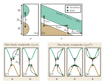
We start by presenting a phenomenological model of Mott insulator as a material with variable concentration of charge carriers. In this model, similarly to electrons and holes in semiconductors, the carriers are doublons and holes, which are one-particle excitations in upper and lower Hubbard bands, respectively, see Fig. 1(a). Note that here we adopt a simplified description and do not consider the dynamical nature of the Mott gap, which is held fixed. Furthermore, we impose the doublon-hole symmetry, such that these excitations differ only for their charge () and have the same concentration , which hereafter is simply referred to as doublon density.
The density of doublon excitations can be considered as a state variable which determines the conductivity of the material. In this phenomenological model, doublons have charge , effective mass and they accelerate in an electric field, before scattering after a typical time . This is formalized in the Drude formula for the conductivity,
| (1) |
which relates the current density to the electric field ,
| (2) |
Similar forms to Eq. (1) also apply to weakly correlated materials, with for example representing the density of conduction-band electrons. The key difference with the model at hand is in the rate equation for , in which the strong correlations typical of Mott materials appear as a non-linear term in the doublon density,
| (3) |
Here the source term describes excitations of doublon-hole pairs induced by thermal fluctuations or quantum tunneling across the gap, see Fig. 1(b). In principle, these depend on temperature and electric field; here we hold fixed and concentrate on the field dependence of the other terms. The second term in Eq. (3) describes the decay of doublon excitations with a typical time [53]. The equilibrium density, namely the zero-field stationary solution, is . The one-body avalanche term (), also known as impact ionization, is present in both strongly [25] and weakly correlated materials [31]. It describes a process in which the kinetic energy of a carrier is converted into excitation energy of new carriers via scattering with impurities or phonons [Fig. 1(c),(d)]. The two-body avalanche term (), on the other hand, describes many-body scatterings of two excitations kicking out new carriers [Fig. 1(e)-(g)] and is therefore proportional to the squared carrier density. The last term describes carrier diffusion due to density gradients; hereafter we consider the homogeneous case .
In nonzero electric field, Eq. (3) yields two stationary doublon densities, that is the solutions of :
| (4) |
Here and is the ratio of the one- to the two-body avalanche term for . Imposing the solutions (4) to be real and positive yields the condition , with the threshold electric field
| (5) |
where the approximation is valid for small , namely for predominant two-body avalanche. At this threshold, the two branches of Eq. (4) merge, the doublon density is
| (6) |
and the current density reads
| (7) |
In contrast with the threshold electric field and doublon density, the threshold current density does not depend on the one-body constant , but only on the two-body constant (through ) and it diverges for .
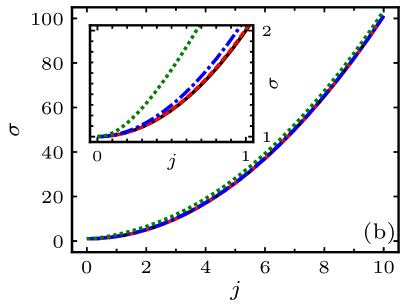
Since the conductivity increases with doublon density, we can interpret the lower branch of Eq. (4) as the slightly perturbed equilibrium insulating state, and the upper branch as a conducting state. The corresponding current density is plotted in Fig. 2(a). It should be stressed that the two branches correspond to the same microscopic state and differ only in the doublon density; in particular, this theory does not cover the field-induced collapse of the Mott gap. Equation (4) also implies that, within this model, there are no stationary solutions for , meaning that the material cannot sustain such electric fields. In Fig. 2(b) we plot the conductivity as a function of the current density,
| (8) |
where is the inverse function of and the approximation is valid for small . Expressions similar to Eq. (8) have been suggested to explain experiments on a class of charge-transfer insulators [7, 32].
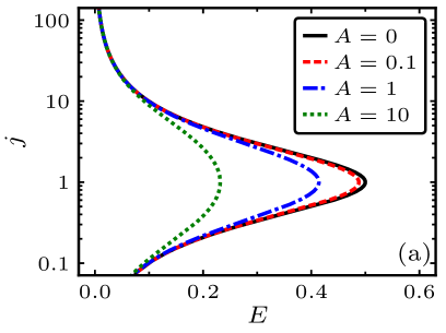
The results in Fig. 2 are in qualitative agreement with experiments in which a current is passed through a Mott insulator and the electric field (thus the conductivity) is measured, see e. g. Refs. [34, 35]. Indeed, up to this point the treatment is suitable to describe situations in which the current, and not the electric field, is the external parameter. To show this from a formal point of view, we linearize Eq. (3) around the stationary solution (4) at fixed or at fixed . In the former case we get which shows that only the lower branch is stable. If we instead fix , we get which is stable for all current densities. Only in the latter case states with large conductivity are stable and can therefore be observed.
Among the parameters introduced in this section, most relevant are , , ; which set the characteristic scales of, respectively, time, electric field, current density. The doublon decay time is typically , as measured in ultrafast pump-probe optical spectroscopy [3, 4, 5, 6], while electric fields of the order and current densities have been measured in Refs. [7, 34, 35]. Together with the physical dimensions of the memristor, and also set the characteristic scales of, respectively, voltage and current.
II Current-voltage characteristic and insulating-conducting transitions
We introduce now our model of Mott memristor as a device composed of a Mott insulator connected in series with a conventional resistor. Adopting the description in Sec. I, the resistance of the Mott insulator is a function of carrier density through the conductivity [Eq. (1)]:
| (9) |
where and are length and section area. Instead, the conventional resistor has a fixed resistance . The total resistance of the memristor, or memristance, is therefore
| (10) |
and the doublon density is its state variable. Attaching a voltage generator to the memristor, the electric field internal to the Mott material is
| (11) |
with , . Thus, the electric field does not depend solely on the applied voltage, but also on the doublon density. For small density the resistance of the Mott material is large, , and the field is approximately proportional to the voltage. On the other hand, for large density the resistance of the Mott material drops, , and so does the field. This mechanism is crucial for the stabilization of the conducting state of the memristor, as we discuss in this section.
The state-dependent resistance [Eq. (10)] and the rate equation for the state variable [Eqs. (3) and (11)] define a non-polar voltage-controlled memristive system [38]. In practice, the fixed term in the resistance corresponds to either the contact resistance, often present especially in two-probe measurements (see e. g. Ref. [33]), or a resistor added to obtain a stable conducting state [7, 34, 35].
II.1 Stationary doublon density
The stationary condition is obtained plugging Eq. (11) into Eq. (3) and imposing (we set hereafter). We solve the resulting equation for :
| (12) |
where . This is plotted in Fig. 3(a) as versus which allows us to visualize the stationary density as a function of voltage. This solution is stable only if , namely for outside a range , where these values are therefore obtained imposing
| (13) |
which yields
| (14) |
For small we can approximate and . Therefore, the two stable branches are well separated () and we can interpret them as the insulating () and conducting () states of the memristor. Increasing the two branches approach each other as and eventually merge for . Beyond this value, we have one continuous stable state with no clear separation between insulating and conducting states. In the opposite limit, , the stable conducting branch vanishes (). In the remainder of this work we set . Between and insulating and conducting states coexist. In particular, to correspond the densities on the insulating branch and on the conducting branch.
II.2 Current-voltage characteristic
In the stationary state with voltage and doublon density , the current through the memristor is
| (15) |
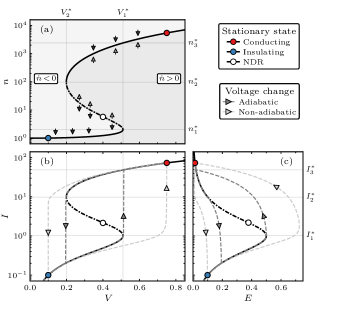
where . Plotting Eq. (15) versus Eq. (12) we obtain the current-voltage curve in Fig. 3(b). This has a distinct “S” shape composed of three branches with alternating differential resistance , which is positive in the stable insulating and conducting branches; and negative in the unstable region in between [negative-differential-resistance region (NDR)].
A voltage sweep across the range results in a current hysteresis, see Fig. 3(b). If the voltage change is adiabatic, meaning so slow that at each moment the memristor is stationary, then from the insulating branch the current follows the - curve up to , where a jump discontinuity leads from to the conducting branch in . Then, upon decreasing the voltage, the current remains large down to where a second discontinuity leads from back to the insulating branch. If the voltage change is non-adiabatic, namely rapidly increasing and decreasing, the current does not follow thoroughly the - curve but instead traces a larger hysteresis area.
In Fig. 3(c) we plot the same quantities as in Fig. 3(b) versus the electric field internal to the Mott insulator. Since current and current density are proportional, , the stationary curve is a rescaled copy of Fig. 2(a) with the crucial difference that this is now stable also for . The trajectories appear different in the plane with respect to the curves; since during the constant-voltage insulating-conducting transitions both current and internal field vary. Also in this case, a non-adiabatic voltage results in a wider trajectory.
II.3 Delay time and relaxation time
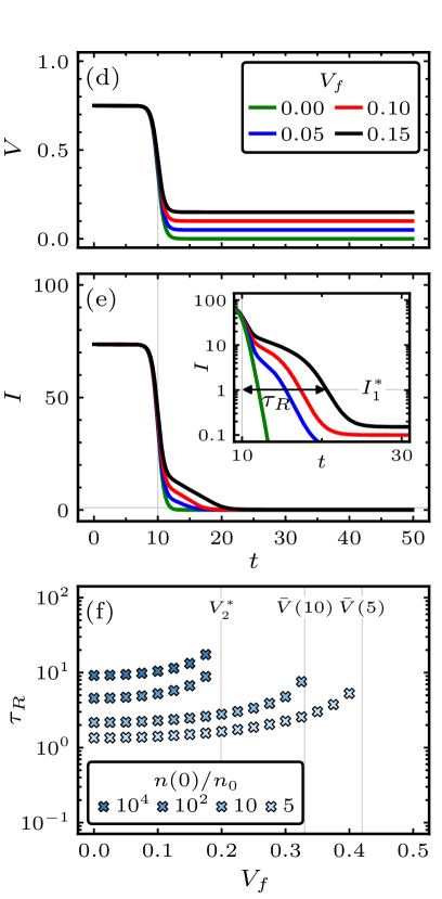
To study the time scales associated with the transitions between insulating and conducting states, we consider a voltage with a ramp function and we numerically integrate Eqs. (3), (11). From the insulating state, as the voltage increases above , the transition takes place in two steps [Fig. 4(a),(b)]: first, during a delay time the current remains low; then, it rapidly increases above , meaning that the memristor has become conducting. Notice that after the transition since in the conducting state the memristance is approximately constant .
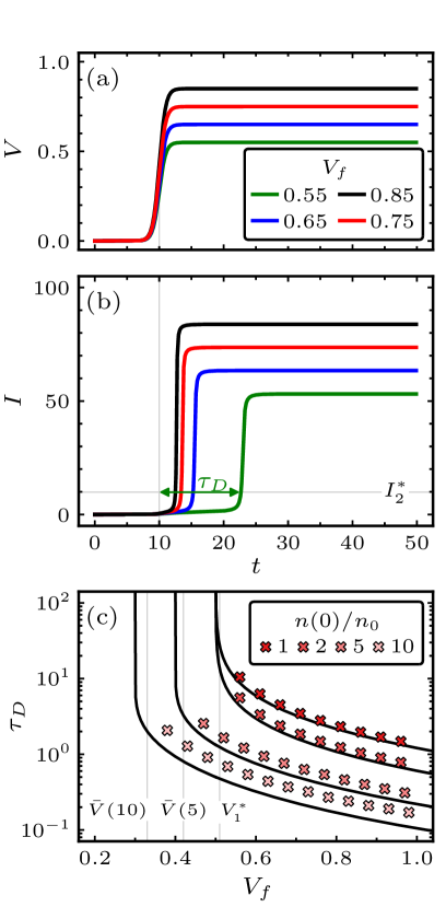
The delay time is plotted in Fig. 4(c) versus the voltage and for varying initial conditions. While the insulting-to-conducting transition naturally starts from the insulating branch , here we consider also initial conditions in the unstable region which are relevant in the case the voltage changes while the memristor is not at equilibrium. The delay time decreases with increasing voltage and larger initial density. It diverges in if the initial density is below , or in otherwise. This difference can be explained with the aid of the stationary curve in Fig. 3(a), which shows that for the minimum voltage leading to the conducting branch is indeed .
To get analytical insight into the delay time and its dependence on voltage and initial density, we solve Eq. (3) in the approximation obtaining for (see Appendix A):
| (16) |
where and . In this approximation the transition to the conducting state happens where Eq. (16) diverges, giving the delay time
| (17) |
which we plot in Fig. 4(c) alongside the numerical result. In the limit we have and . The behavior of depends on whether is smaller or larger than , in the former case it diverges as , while in the latter case it stays finite and diverges at a lower voltage .
Also the transition from the conducting state, as the voltage decreases below , takes place in various steps [Fig. 4(d),(e)]: first, the current rapidly decreases; then, it remains high during a relaxation time ; finally, it decreases below . The relaxation time is plotted in Fig. 4(f) versus the voltage and for varying initial conditions. Analogously to what discussed for the delay time, we consider initial conditions in the conducting branch as well as in the unstable region . The relaxation time increases with increasing voltage and larger initial density; and diverges in if the initial density is above , or in otherwise.
The results in this section, in particular the current-voltage characteristic and the delay time, qualitatively agree with various experiments on similar devices [7, 32, 8, 33, 34, 35]. Moreover, the analysis of delay and relaxation times sets the stage for the discussion of the a. c. response, a fundamental characteristic of a memristive system.
III Response to alternating voltage
We proceed now with the study of the a. c. response of the Mott memristor introduced in Sec. II and defined by its state-dependent resistance and state-variable equation of motion [Eqs. (3), (9)-(11)], including the typical memristive features of current retardation and current-voltage pinched hysteresis loop.
III.1 Time evolution of doublon density and steady-state current
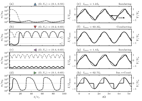
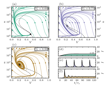
In Fig. 5(a)-(d) we plot the time evolution of doublon density [obtained by numerical integration of Eqs. (3) and (11)] for various amplitude and frequency of the voltage and for two different initial conditions. We distinguish four qualitatively different steady states. In Fig. 5(a),(b) the steady state is respectively insulating () or conducting () independently of the initial condition. In contrast, in the case of Fig. 5(c) there are two possible steady states depending on the initial condition. Finally, in Fig. 5(d) the steady state goes back and forth the insulating and conducting states.
The corresponding steady-state current is plotted in Fig. 5(e)-(h) for the insulating initial condition and alongside the voltage. The time axis is rescaled with the period and the current and voltage axes with their maxima, for the purpose of comparing various choices of parameters. The insulating steady state [Fig. 5(e),(g)] shows a clear retardation, namely the current profile is distorted with respect to the sinusoidal voltage. Such a retardation effect is the hallmark of memristive systems (see e. g. Ref. [40]) as it exemplifies the inertial change of instantaneous resistance. The effect almost vanishes in the conducting steady state [Fig. 5(f)] because in this case the memristance is approximately constant . Finally, in the steady state back and forth insulating and conducting [Fig. 5(h)] the retardation is very pronounced; in this case the voltage effectively acts as an adiabatic switch, as we discuss below in more detail.
III.2 Current-voltage pinched hysteresis loop and charge-flux relation
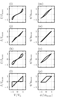
In Fig. 5(i)-(l) we plot the steady-state current versus the voltage. This curve traces a pinched hysteresis loop (so called because it crosses the coordinate axes only in the origin) which is considered the empirical definition of a memristive system [38]. Also here, we have rescaled the axes for the sake of comparing the different steady states. The curve slope is the instantaneous inverse differential resistance , meaning that the greater the resistance change, the larger the area encircled by the loop. Indeed, this is more evident in the insulating state [Fig. 5(i),(k)] than in the conducting state [Fig. 5(j)] which has almost constant resistance. In the steady state back and forth insulating and conducting [Fig. 5(l)] the loop is composed of flat, vertical and steep segments. These correspond to, respectively, insulating state, insulating-to-conducting transition, conducting state; while the conducting-to-insulating transition happens near the origin [cf. arrows in Fig. 5(l)].
The direction of the loop, namely whether it is traced clockwise or anti-clockwise, is related to the polarity of the memristive system. In bipolar memristors, e. g. based on ionic drift [40], the resistance changes depending on the sign of the input. Consequently, it is either maximum or minimum in the origin of the plane, and the loop is anti-clockwise for positive and clockwise for negative input. In contrast, in the present case the memristor is non-polar, meaning the resistance change is independent of the sign of the input, cf. Eq. (3). As a result, the loop is anti-clockwise both for positive and negative inputs [see arrows in Fig. 5(k),(l)]. Moreover, this implies that the slope in the origin, namely the zero-voltage inverse instantaneous resistance, is the same for increasing or decreasing voltage.
Other characteristics of a memristive system are more conveniently discussed in terms of the relation between charge and flux , namely the integrals of, respectively, current and voltage. Indeed, originally the memristance was introduced as the quantity relating flux to charge [] similarly to how the resistance relates voltage to current [] [37]. The steady-state charge-flux relation is plotted in Fig. 5(m)-(p). The multivaluedness of this relation is the empirical evidence that the memristive system belongs to the class of non-ideal memristors [38]. For ideal memristors, the state-variable equation of motion depends on the input only [] giving a unique relation between charge and flux [37, 40]. Instead, in the broader class of non-ideal memristors, the equation of motion depends also on the state variable itself [] which yields a multivalued charge-flux relation, as in the this case. On a practical level, an ideal memristor is non-volatile, meaning its state does not change on zero input [], while the state of a non-ideal memristor typically relaxes [] which makes it a volatile memory.
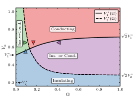
III.3 Steady-state diagram
In Fig. 6 we plot the steady-state diagram as a function of voltage frequency and amplitude. This contains four regions, delimited by the frequency-dependent amplitude thresholds , corresponding to each of the steady states discussed above:
- 1.
-
2.
For amplitude larger than (red region) the steady state is conducting, as in Fig. 5(b).
-
3.
For frequency not too low and amplitude within the range (purple region) the steady state is insulating or conducting depending on the initial condition, as in Fig. 5(c).
-
4.
For low frequency and amplitude within the range (green region) the steady state goes back and forth insulating and conducting, as in Fig. 5(d).
The a. c. thresholds are closely related to the d. c. thresholds of Sec. II. If we apply a voltage with small amplitude, such that the memristor is insulating, and then gradually increase it, is the minimum value at which the memristor becomes conducting. Notice the analogy with , which is the minimum voltage to trigger the d. c. insulating-to-conducting transition. However, in the a. c. case two scenarios are possible: the memristor either stays conducting indefinitely, or it goes back to insulating at a later point of the voltage period. The two regions above (respectively red and green in Fig. 6) correspond to these two cases. Analogously, applying a voltage with large amplitude, such that the memristor is conducting, and then gradually decreasing it, is the amplitude at which the memristor becomes insulating.
To discuss the frequency dependence of , it is convenient to separately consider the regimes of low, intermediate, and high frequency.
III.3.1 Low frequency
At low frequency, the a. c. response to a voltage is in a sense singular. On the one hand, at zero frequency the voltage reduces to constant. On the other hand, at non-zero albeit low frequency, it successively assumes all values in . In other words, in the low-frequency limit the a. c. voltage is equivalent to an adiabatic sweep, such as considered in Sec. II. Thus, the steady state is insulating if and back and forth insulating and conducting if , as for repeated sweeps, cf. Fig. 3(b). Note the absence of conducting steady states in this limit, since no matter how large the amplitude, the memristor invariably turns insulating during the long interval in which the voltage assumes low values. This is reflected in the divergence of , while is continuous and tends to the d. c. threshold .
III.3.2 Intermediate frequency
The intermediate-frequency regime can be understood in terms of a competition of time scales: the half-period ; and the delay () and relaxation () times, namely the time scales for, respectively, the insulating-to-conducting and the conducting-to-insulating transitions. While these were precisely defined in Sec. II for the d. c. transitions, here the discussion is more qualitative and depends only on being, respectively, decreasing and increasing as a function of voltage amplitude.
Since within the range (green region in Fig. 6) there are one insulating-to-conducting and one conducting-to-insulating transition during each half a period [cf. Fig. 5(d),(h)], this region is characterized by the relation . Indeed, if either time scale were longer than , the corresponding transition could not take place. This suggests the interpretation of as the curves where, respectively, and . Crossing for example , the region with insulating steady states is characterized by , that is by the inhibition of the insulating-to-conducting transition. Within this perspective, increases with frequency because – as decreases – a larger voltage amplitude is needed to match the condition .
Where intersect each other, the time scales are all equal: . Crossing this point at constant voltage amplitude, becomes at the same time shorter than both , meaning that both the insulting-to-conducting and the conducting-to-insulating transitions are inhibited, and the memristor remains in the same state as the initial condition (purple region in Fig. 6).
III.3.3 High frequency
The behavior at high frequency is better illustrated in terms of the infinite-frequency limit, in which the voltage is equivalent to a d. c. . Indeed, the voltage enters the equation of motion [Eqs. (3), (11)] through the square which at high frequency is equivalent to its average . The steady state is therefore insulating if and conducting if . Similarly to the d. c. coexistence region, in the range the steady state is insulating or conducting depending on the initial condition. Note that in the high-frequency limit tend to constant. To reconcile this with the previous discussion in terms of time scales, we have to consider that at high frequency the transitions can happen across multiple voltage periods.
IV Self-sustained oscillations and spiking behavior
We study now a first use case of the Mott memristor in electric circuits. In the circuit in Fig. 7(a) the memristor is connected in parallel with a capacitor and is attached to a voltage generator through a load resistor . This setup allows us to study self-sustained current oscillations as observed, e. g., in Refs. [33, 34, 35]; a phenomenon at the basis of spiking-based computational schemes.
IV.1 Nullclines and fixed point
The equation for the voltage across the memristor is obtained applying Kirchhoff’s law of current conservation at the nodes of the circuit in Fig. 7(a):
| (18) |
which are the currents through, respectively, capacitor, memristor and voltage generator. Equation (18) has to be solved together with the rate equation for the doublon density [Eqs. (3), (11)]. Defining , and the time scale we rewrite these equations as a dynamical system
| (19a) | ||||
| (19b) | ||||
The fixed point of this system is at the intersection of the so-called nullclines, namely the curves along which and , which read respectively
| (20a) | ||||
| (20b) | ||||
We subtract now the nullclines and, similarly to Sec. II, we solve the resulting equation for , thereby expressing the fixed-point doublon density as the inverse function of
| (21) |
This can also be obtained imposing the intersection of the so-called load line with the curve of the Mott memristor [Eqs. (12), (15)], see Fig. 7(b), since at the fixed point the same current flows through voltage generator and memristor [cf. Eq.(18) with ].
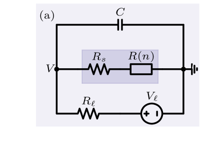
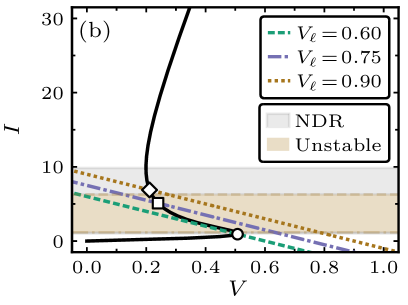
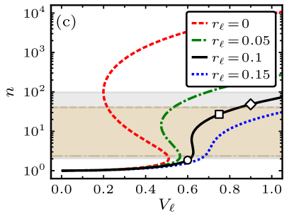
Because the current through the capacitor is zero at the fixed point, the resistances and are in series and the circuit reduces to the situation considered in Sec. II with the substitutions and , which indeed make Eq. (21) identical to Eq. (12). Therefore, the same analysis applies here: if the solution is unique, while if there is a region with three solutions, see Fig. 7(c). Together with , we set hereafter which gives .
Depending on load voltage and load resistor, the fixed point can be in the NDR region of the Mott memristor, see Fig. 7(b)-(d), which is necessary for having limit-cycle self-sustained oscillations, as we discuss in the following.
IV.2 Limit-cycle oscillations
Self-sustained oscillations are periodic solutions of a dynamical system, such as Eqs. (19), in absence of any periodic input. In the system configuration space (here the plane) the corresponding trajectories are limit cycles, namely isolated closed trajectories which either attract or repel nearby ones [54]. Simply stated, the conditions for a limit cycle are the non-linearity of the system and the instability of its fixed point. In this case, the former is provided by the non-linear rate equation for the doublon density. The latter is satisfied if the fixed-point doublon density is between the values (see Appendix B)
| (22) |
Once the load voltage – thus the fixed-point doublon density – is chosen, Eq. (22) gives an implicit expression for the critical , which varies with the fixed-point doublon density and whose minimum is obtained setting to zero the argument of the square root in Eq. (22):
| (23) |
The region is included in the NDR region of the memristor, coinciding with it in the limit of large . As depicted in Fig. 7(d), to enter this region one can either tune the load voltage (thus the doublon density) or the capacitor (thus the characteristic time ). At this point, a supercritical Hopf bifurcation takes place [54], namely the fixed point loses stability and a limit cycle arises.
IV.2.1 Tuning the load voltage
At fixed we consider three load voltages such that the fixed-point doublon density is below, inside, or above the unstable region , see Fig. 7(b)-(d). For each load voltage we numerically integrate Eqs. (19) with varying initial conditions and plot the trajectories in the plane in Fig. 8(a)-(c). Outside the unstable region () all trajectories tend to the fixed point. Notice that this implies the absence of closed trajectories. In stark contrast, inside the unstable region () there is an isolated closed trajectory (i. e. a limit cycle) which attracts all other trajectories. Notice that the limit cycle is around the unstable fixed point. In this case there is no stationary stable solution and, despite the constant load voltage, density and voltage oscillate indefinitely. In other words, the system undergoes limit-cycle self-sustained (or autonomous) oscillations.
The current profile is markedly different in the three cases. Let us consider [see Fig. 8(d)-(f)] the trajectories with initial condition . For the current increases monotonically to the stable fixed point, which is on the insulating branch, see Fig. 8(d). In contrast, for the stable fixed point is near the conducting branch and is reached only after a transient, which in the plane takes the form of a spiral around the fixed point [Fig. 8(c)], and the current profile has a single spike followed by damped oscillations, see Fig. 8(f).
Finally, corresponding to the limit cycle, for the current has periodic spiking, see Fig. 8(e). Each spike consists of a sudden increase and a similarly rapid, but slower, decrease. These are due to repeated transitions between the memristor insulating and conducting states, Note that this is consistent with the spiking behavior of biological neurons, in which the neural-cell membrane also transitions between insulating and conducting in the course of an oscillation [55].
IV.2.2 Tuning the capacitor
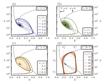
In Fig. 9 we plot the trajectories obtained by numerical solution of Eqs. (19) with initial condition , fixed load voltage and varying . With its location unaltered, the fixed point loses stability across a critical (for ), see Fig. 7(d). It is stable for and reached after a number of oscillations which become more dense as is approached. As soon as , the fixed point becomes unstable and a small limit cycle appears. Increasing further, the limit cycle grows and tends to a loop with segments at constant voltage connecting lower and upper branches of the nullcline, see Fig. 9(d). Since this nullcline is nothing but the stationary doublon density versus the voltage [cf. Fig. 3(a)] this limit cycle is equivalent to the hysteresis loop in adiabatic voltage considered in Sec. II. In other words, in this limit the circuit behaves like a relaxation oscillator [54].
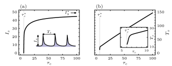
The limit-cycle current spikes can be characterized by height (difference between maximum and minimum) and period, see Fig. 10. Evidently, these quantities are only defined for . At we have the typical behavior for a supercritical Hopf bifurcation [54]: the height grows from zero (the limit cycle has vanishing amplitude) while the period is finite and equal to , with the Jacobian of the dynamical system (19) at the fixed point (see Appendix B). Increasing , the height first rapidly increases, then it slowly saturates to a value close to which is, together with , the stationary current at the threshold voltage , cf. Fig. 3(b). At the same time, already at , the period is linear in , showing a decoupling of time scales for doublon density and voltage, as expected for a relaxation oscillator.
Conclusions
We have proposed the narrow-gap Mott insulator as a compact realization of a new type of memristor based on the field-induced carrier avalanche multiplication. Due to this purely electronic mechanism for the resistive switch, this Mott memristor has a characteristic time scale set by the doublon-excitation decay time , which is up to several orders of magnitude faster than in devices based on Joule heating or ionic drift.
As a first step we have put forward a phenomenological description of the field-induced carrier avalanche in Mott insulators, in which the conductivity depends on the carrier density, whose rate equation contains the non-linear scattering terms induced by strong correlations. Building on this, we have introduced the Mott memristor as a device made of a Mott material in series with a conventional resistor; and we have derived its current-voltage curve, as well as the transitions between conducting and insulating states. While the very definition qualifies the model as a non-polar, voltage-controlled memristive system, we have analyzed in detail its a. c. response, in particular the pinched hysteresis loop and the steady-state diagram as a function of amplitude and frequency. Finally, we have considered a circuit with a capacitor in parallel with the Mott memristor, and demonstrated self-sustained current oscillations and periodic spiking behavior, consistent with the periodic activity of biological neurons.
While similar devices have been subject of intensive experimental study [7, 32, 8, 33, 34, 35], this is the first time (to the best of our knowledge) they are proposed as memristors. Moreover, our work provides a comprehensive theory of the key features of those prior studies: threshold electric field, negative differential resistance (NDR), multivalued current-voltage characteristic, delay time, and current oscillations. At the same time, our proposal consists of a tractable set of equations; which stands in contrast with previous more complicated models, see e. g. Ref. [47], and results in two valuable features. First, it allowed us to derive analytical expressions, such as the boundaries of the NDR region and the conditions for limit-cycle oscillations. Second, and perhaps more importantly, it makes promising to include the model into the description of circuits of growing complexity, in the quest for bio-inspired novel computing architectures.
Appendix A Derivation of Eqs. (16) and (17)
In this appendix we derive Eqs. (16), (17) of Sec. II for doublon density and delay time of the d. c. insulating-to-conducting transition. To simplify the exposition, we set , . Then Eq. (3) is rewritten as
| (24) |
The two stationary solutions are where and [cf. Eq. (4)] and are real only if [cf. Eq. (5)]. Since during the delay time the doublon density does not change much, we approximate the field in the Mott insulator as constant, , which is equivalent to approximating , yielding and . Equation (24) can then be solved with a variable change:
| (25) | |||
| (26) |
The general solution of the transformed equation (26) is where . Substituting this back into (25) yields the solution of Eq. (24):
| (27) |
Notice that the solution of (26) depends on both while Eq. (27) depends only on their ratio. To proceed, we parametrize and obtain
| (28) | |||
| (29) |
Up to now we have considered the electric field above threshold , which is equivalent to and makes and Eqs.(28), (29) real. In the limit we have , and the behavior of the delay time Eq. (29) depends on the initial condition:
| (30) |
Indeed with a large initial density the transition happens even below threshold. In this case we have to choose differently or, alternatively, we can analytically continue Eqs. (28), (29) with which yields
| (31) | |||
| (32) |
In this case the delay time diverges for , namely for , as shown in Fig. 4(c).
Appendix B Derivation of Eq. (22)
In this appendix we derive Eq. (22) for the region with limit cycle in Sec. IV. A limit cycle is guaranteed to exist by the Poincaré–Bendixson theorem when the system is confined in a region with no stable fixed point therein [54]. Such a trapping region is (with ) . The fixed point turns from stable to unstable (Hopf bifurcation) when, with positive determinant, the trace of the Jacobian becomes positive. For the system (19) the Jacobian reads
| (33) |
Plugging Eq. (20b) for the nullcline into Eq. (33), we obtain the Jacobian as a function of the fixed-point doublon density:
| (34) |
whose determinant and trace read
| (35) | |||
| (36) |
The sign of the determinant does not depend on and is positive for outside the range with . The sign of the trace depends on . Notice that a necessary condition for the trace to vanish is which is the same condition for the NDR region of the memristor, cf. Eq. (13), demonstrating that the region with limit-cycle oscillations is a subset of the NDR region, as depicted in Fig. 7(b)-(d). Imposing the trace to be positive we get the condition that should be outside the range with given in Eq. (22).
References
- Imada et al. [1998] M. Imada, A. Fujimori, and Y. Tokura, Metal-insulator transitions, Rev. Mod. Phys. 70, 1039 (1998).
- Lee et al. [2006] P. A. Lee, N. Nagaosa, and X.-G. Wen, Doping a Mott insulator: physics of high-temperature superconductivity, Rev. Mod. Phys. 78, 17 (2006).
- Iwai et al. [2003] S. Iwai, M. Ono, A. Maeda, H. Matsuzaki, H. Kishida, H. Okamoto, and Y. Tokura, Ultrafast optical switching to a metallic state by photoinduced Mott transition in a halogen-bridged nickel-chain compound, Phys. Rev. Lett. 91, 057401 (2003).
- Perfetti et al. [2006] L. Perfetti, P. Loukakos, M. Lisowski, U. Bovensiepen, H. Berger, S. Biermann, P. Cornaglia, A. Georges, and M. Wolf, Time evolution of the electronic structure of 1T-TaS2 through the insulator-metal transition, Phys. Rev. Lett. 97, 067402 (2006).
- Okamoto et al. [2007] H. Okamoto, H. Matsuzaki, T. Wakabayashi, Y. Takahashi, and T. Hasegawa, Photoinduced metallic state mediated by spin-charge separation in a one-dimensional organic Mott insulator, Phys. Rev. Lett. 98, 037401 (2007).
- Okamoto et al. [2010] H. Okamoto, T. Miyagoe, K. Kobayashi, H. Uemura, H. Nishioka, H. Matsuzaki, A. Sawa, and Y. Tokura, Ultrafast charge dynamics in photoexcited Nd2CuO4 and La2CuO4 cuprate compounds investigated by femtosecond absorption spectroscopy, Phys. Rev. B 82, 060513 (2010).
- Tokura et al. [1988] Y. Tokura, H. Okamoto, T. Koda, T. Mitani, and G. Saito, Nonlinear electric transport and switching phenomenon in the mixed-stack charge-transfer crystal tetrathiafulvalene-p-chloranil, Phys. Rev. B 38, 2215 (1988).
- Taguchi et al. [2000] Y. Taguchi, T. Matsumoto, and Y. Tokura, Dielectric breakdown of one-dimensional Mott insulators Sr2CuO3 and SrCuO2, Phys. Rev. B 62, 7015 (2000).
- Fursina et al. [2009] A. Fursina, R. Sofin, I. Shvets, and D. Natelson, Origin of hysteresis in resistive switching in magnetite is Joule heating, Phys. Rev. B 79, 245131 (2009).
- Zimmers et al. [2013] A. Zimmers, L. Aigouy, M. Mortier, A. Sharoni, S. Wang, K. West, J. Ramirez, and I. K. Schuller, Role of thermal heating on the voltage induced insulator-metal transition in VO2, Phys. Rev. Lett. 110, 056601 (2013).
- Cario et al. [2010] L. Cario, C. Vaju, B. Corraze, V. Guiot, and E. Janod, Electric-field-induced resistive switching in a family of Mott insulators: Towards a new class of RRAM memories, Adv. Mat. 22, 5193 (2010).
- Guiot et al. [2013] V. Guiot, L. Cario, E. Janod, B. Corraze, V. T. Phuoc, M. Rozenberg, P. Stoliar, T. Cren, and D. Roditchev, Avalanche breakdown in GaTa4Se8-xTex narrow-gap Mott insulators, Nat. Commun. 4, 1 (2013).
- Nakamura et al. [2013] F. Nakamura, M. Sakaki, Y. Yamanaka, S. Tamaru, T. Suzuki, and Y. Maeno, Electric-field-induced metal maintained by current of the Mott insulator Ca2RuO4, Sci. Rep. 3, 2536 (2013).
- Stoliar et al. [2013] P. Stoliar, L. Cario, E. Janod, B. Corraze, C. Guillot-Deudon, S. Salmon-Bourmand, V. Guiot, J. Tranchant, and M. Rozenberg, Universal electric-field-driven resistive transition in narrow-gap Mott insulators, Adv. Mater. 25, 3222 (2013).
- Yamakawa et al. [2017] H. Yamakawa, T. Miyamoto, T. Morimoto, T. Terashige, H. Yada, N. Kida, M. Suda, H. Yamamoto, R. Kato, K. Miyagawa, et al., Mott transition by an impulsive dielectric breakdown, Nat. Mater. 16, 1100 (2017).
- Giorgianni et al. [2019] F. Giorgianni, J. Sakai, and S. Lupi, Overcoming the thermal regime for the electric-field driven Mott transition in vanadium sesquioxide, Nat. Commun. 10, 1159 (2019).
- Kalcheim et al. [2020] Y. Kalcheim, A. Camjayi, J. del Valle, P. Salev, M. Rozenberg, and I. K. Schuller, Non-thermal resistive switching in Mott insulator nanowires, Nat. Commun. 11, 1 (2020).
- Zhang et al. [2019] J. Zhang, A. S. McLeod, Q. Han, X. Chen, H. A. Bechtel, Z. Yao, S. G. Corder, T. Ciavatti, T. H. Tao, M. Aronson, et al., Nano-resolved current-induced insulator-metal transition in the Mott insulator Ca2RuO4, Phys. Rev. X 9, 011032 (2019).
- Woynarovich [1982a] F. Woynarovich, Excitations with complex wavenumbers in a Hubbard chain. I. States with one pair of complex wavenumbers, J. Phys. C: Solid State Phys. 15, 85 (1982a).
- Woynarovich [1982b] F. Woynarovich, Excitations with complex wavenumbers in a Hubbard chain. II. States with several pairs of complex wavenumbers, J. Phys. C: Solid State Phys. 15, 97 (1982b).
- Oka et al. [2003] T. Oka, R. Arita, and H. Aoki, Breakdown of a Mott insulator: a nonadiabatic tunneling mechanism, Phys. Rev. Lett. 91, 066406 (2003).
- Oka and Aoki [2005] T. Oka and H. Aoki, Ground-state decay rate for the Zener breakdown in band and Mott insulators, Phys. Rev. Lett. 95, 137601 (2005).
- Eckstein et al. [2010] M. Eckstein, T. Oka, and P. Werner, Dielectric breakdown of Mott insulators in dynamical mean-field theory, Phys. Rev. Lett. 105, 146404 (2010).
- Oka [2012] T. Oka, Nonlinear doublon production in a Mott insulator: Landau-Dykhne method applied to an integrable model, Phys. Rev. B 86, 075148 (2012).
- Werner et al. [2014] P. Werner, K. Held, and M. Eckstein, Role of impact ionization in the thermalization of photoexcited Mott insulators, Phys. Rev. B 90, 235102 (2014).
- Stoliar et al. [2014] P. Stoliar, M. Rozenberg, E. Janod, B. Corraze, J. Tranchant, and L. Cario, Nonthermal and purely electronic resistive switching in a Mott memory, Phys. Rev. B 90, 045146 (2014).
- Li et al. [2015] J. Li, C. Aron, G. Kotliar, and J. E. Han, Electric-field-driven resistive switching in the dissipative Hubbard model, Phys. Rev. Lett. 114, 226403 (2015).
- Mazza et al. [2016] G. Mazza, A. Amaricci, M. Capone, and M. Fabrizio, Field-driven Mott gap collapse and resistive switch in correlated insulators, Phys. Rev. Lett. 117, 176401 (2016).
- Li et al. [2017] J. Li, C. Aron, G. Kotliar, and J. E. Han, Microscopic theory of resistive switching in ordered insulators: electronic versus thermal mechanisms, Nano Lett. 17, 2994 (2017).
- Han et al. [2018] J. E. Han, J. Li, C. Aron, and G. Kotliar, Nonequilibrium mean-field theory of resistive phase transitions, Phys. Rev. B 98, 035145 (2018).
- Hirori et al. [2011] H. Hirori, K. Shinokita, M. Shirai, S. Tani, Y. Kadoya, and K. Tanaka, Extraordinary carrier multiplication gated by a picosecond electric field pulse, Nat. Commun. 2, 1 (2011).
- Iwasa et al. [1989] Y. Iwasa, T. Koda, S. Koshihara, Y. Tokura, N. Iwasawa, and G. Saito, Intrinsic negative-resistance effect in mixed-stack charge-transfer crystals, Phys. Rev. B 39, 10441 (1989).
- Sawano et al. [2005] F. Sawano, I. Terasaki, H. Mori, T. Mori, M. Watanabe, N. Ikeda, Y. Nogami, and Y. Noda, An organic thyristor, Nature 437, 522 (2005).
- Kishida et al. [2009] H. Kishida, T. Ito, A. Nakamura, S. Takaishi, and M. Yamashita, Current oscillation originating from negative differential resistance in one-dimensional halogen-bridged nickel compounds, J. Appl. Phys. 106, 016106 (2009).
- Kishida et al. [2011] H. Kishida, T. Ito, A. Ito, and A. Nakamura, Room-temperature current oscillation based on negative differential resistance in a one-dimensional organic charge-transfer complex, Appl. Phys. Express 4, 031601 (2011).
- Wang et al. [2020] Z. Wang, H. Wu, G. W. Burr, C. S. Hwang, K. L. Wang, Q. Xia, and J. J. Yang, Resistive switching materials for information processing, Nat. Rev. Mater. 5, 173 (2020).
- Chua [1971] L. Chua, Memristor-the missing circuit element, IEEE Trans. Circuit Theory 18, 507 (1971).
- Chua and Kang [1976] L. O. Chua and S. M. Kang, Memristive devices and systems, Proc. IEEE 64, 209 (1976).
- Chua [2011] L. Chua, Resistance switching memories are memristors, Appl. Phys. A 102, 765 (2011).
- Strukov et al. [2008] D. B. Strukov, G. S. Snider, D. R. Stewart, and R. S. Williams, The missing memristor found, Nature 453, 80 (2008).
- Yang et al. [2013] J. J. Yang, D. B. Strukov, and D. R. Stewart, Memristive devices for computing, Nat. Nanotech. 8, 13 (2013).
- Prezioso et al. [2015] M. Prezioso, F. Merrikh-Bayat, B. Hoskins, G. C. Adam, K. K. Likharev, and D. B. Strukov, Training and operation of an integrated neuromorphic network based on metal-oxide memristors, Nature 521, 61 (2015).
- Ielmini and Wong [2018] D. Ielmini and H.-S. P. Wong, In-memory computing with resistive switching devices, Nat. Electron. 1, 333 (2018).
- Kendall and Kumar [2020] J. D. Kendall and S. Kumar, The building blocks of a brain-inspired computer, Appl. Phys. Rev. 7, 011305 (2020).
- Zhu et al. [2020] J. Zhu, T. Zhang, Y. Yang, and R. Huang, A comprehensive review on emerging artificial neuromorphic devices, Appl. Phys. Rev. 7, 011312 (2020).
- Pickett and Williams [2012] M. D. Pickett and R. S. Williams, Sub-100 fJ and sub-nanosecond thermally driven threshold switching in niobium oxide crosspoint nanodevices, Nanotechnology 23, 215202 (2012).
- Pickett et al. [2013] M. D. Pickett, G. Medeiros-Ribeiro, and R. S. Williams, A scalable neuristor built with Mott memristors, Nat. Mater. 12, 114 (2013).
- Kumar et al. [2017a] S. Kumar, J. P. Strachan, and R. S. Williams, Chaotic dynamics in nanoscale NbO2 Mott memristors for analogue computing, Nature 548, 318 (2017a).
- Kumar et al. [2017b] S. Kumar, Z. Wang, N. Davila, N. Kumari, K. J. Norris, X. Huang, J. P. Strachan, D. Vine, A. D. Kilcoyne, Y. Nishi, et al., Physical origins of current and temperature controlled negative differential resistances in NbO2, Nat. Commun. 8, 1 (2017b).
- Kumar et al. [2020] S. Kumar, R. S. Williams, and Z. Wang, Third-order nanocircuit elements for neuromorphic engineering, Nature 585, 518 (2020).
- del Valle et al. [2020] J. del Valle, P. Salev, Y. Kalcheim, and I. K. Schuller, A caloritronics-based Mott neuristor, Sci. Rep. 10, 1 (2020).
- Tang et al. [2016] S. Tang, F. Tesler, F. G. Marlasca, P. Levy, V. Dobrosavljević, and M. Rozenberg, Shock waves and commutation speed of memristors, Phys. Rev. X 6, 011028 (2016).
- Strohmaier et al. [2010] N. Strohmaier, D. Greif, R. Jördens, L. Tarruell, H. Moritz, T. Esslinger, R. Sensarma, D. Pekker, E. Altman, and E. Demler, Observation of elastic doublon decay in the Fermi-Hubbard model, Phys. Rev. Lett. 104, 080401 (2010).
- Strogatz [2018] S. H. Strogatz, Nonlinear dynamics and chaos (CRC press, 2018).
- Izhikevich [2007] E. M. Izhikevich, Dynamical systems in neuroscience (MIT press, 2007).