Thickness-Dependent Band Gap Modification in BaBiO3
Abstract
The material BaBiO3 is known for its insulating character. However, for thin films, in the ultra-thin limit, metallicity is expected because BaBiO3 is suggested to return to its undistorted cubic phase where the oxygen octahedra breathing mode will be suppresse as reported recently. Here, we confirm the influence of the oxygen breathing mode on the size of the band gap. The electronic properties of a BaBiO3 thickness series are studied using in-situ scanning tunneling microscopy. We observe a wide-gap ( 1.2 V) to small-gap ( 0.07 eV) semiconductor transition as a function of a decreasing BaBiO3 film thickness. However, even for an ultra-thin BaBiO3 film, no metallic state is present. The dependence of the band gap size is found to be coinciding with the intensity of the Raman response of the breathing phonon mode as a function of thickness.
The material system BaBiO3 (BBO) received a lot of attention since it was first fabricated in 1963 [1] and is currently applied in various fields as in photoelectrochemical water splitting processes [2] and as an absorber in solar cells [3]. In a simple ionic picture, a Bi4+ ion is expected to be present. Its half-filled 6s shell would make BBO metallic [4, 5, 6, 7]. Contrary, experimental results showed an insulating character [7, 8, 9] with an optically observed bulk band gap of 2 eV [10, 11, 12], raising the question what mechanism is responsible for its insulating behavior. When more studies were performed, it was discovered that BBO became superconducting upon hole doping [4, 5, 6, 12, 13, 14]. With optimum lead or potassium doping, critical temperatures of 13 K [6] and 30 K [14], respectively, were achieved. It is still an open question why BaPb1-xBixO3 and Ba1-xKxBiO3 become superconducting. A possible explanation might be related to the mechanism causing the unexpected insulating behavior in BBO. In this work, the electronic properties are studied to shine a new light on the mechanism responsible for the insulating character.
At first, a charge disproportionation, with alternating 3+ and 5+ valence states of the Bi atom, was given as the origin for the insulating behavior [7, 10, 15, 16]. Subsequently, others claimed the oxygen breathing mode [8, 11, 17, 18] – where the oxygen octahedra contract and expand – to be responsible for the band gap formation in BBO. In a more recent view, a strong hybridization between the Bi 6s and O 2p states creates a bond disproportionation [19, 20, 21]. Here, all bismuth ions have an oxidation state of 3+ [21, 22], but different local environments. A hole pair sits on the contracted oxygen octahedra [21], explaining the experimentally observed two different Bi-O bond lengths [7, 10, 15]. In experimental work, the presence of an oxygen 2p hole density in the ground state was observed for BBO single crystals [23] and a Bi core level analysis of BBO thin films revealed the presence of solely Bi3+ ions [24], both agreeing with the theoretically proposed bond disproportionated picture.
In both the charge disproportionated and bond disproportionated picture, the oxygen octahedra breathing mode is present. The appearance of this breathing mode combined with octahedra tilting distortions cause a phase transition from a cubic to a monoclinic structure [16]. When considering the thickness of the BBO films as a degree of freedom, it was found that for films thinner than 9 unit cells (u.c.) the structure transforms from a tetragonal to a cubic phase [25], hinting towards a suppression of the oxygen breathing mode. Theory shows a closing of the band gap when the oxygen octahedra breathing mode is excluded and a cubic BBO crystal structure is considered [21]. Nevertheless, no electrical properties were determined for any of these ultra-thin BBO films in order to confirm the presence or absence of a thickness-dependent insulator-to-metal transition.
Furthermore, with a Raman spectroscopy experiment on the same series of BBO films, a suppression of the breathing phonon intensity was observed as a function of thickness. Repeating the experiment for BBO films deposited on a double buffer layer template of BaZrO3 and BaCeO3, a suppression of the breathing phonon intensity was not observed until 6 u.c. [26]. When BBO films were deposited directly on a Nb-doped SrTiO3(001) substrate, the breathing phonon intensity was present till a thickness of 7 u.c. [27]. However, it was concluded that the loss of response intensity was caused by a reconstruction layer at the interface (see refs. [28] and [29]), rather than by suppression of the oxygen breathing mode.
Here, we study the electronic properties of a BBO thickness series by in-situ scanning tunneling spectroscopy (STS) experiments. We found that the size of the band gap () depends on the thickness of the BBO film and shrinks from 1.2 V for a 16-unit-cell-thick film to 0.07 eV for a film with a thickness of 3 unit cells. A c(4 2) surface reconstruction confirms the presence of a perovskite structure.
BBO films are fabricated with thicknesses () of 4, 10 and 16 u.c. on TiO2-terminated, 0.5 wt% Nb-doped SrTiO3(001) substrates (Nb:STO) from CrysTec GmbH. The films were fabricated by pulsed laser deposition (PLD) using a stoichiometric house-made BaBiO3 target (purity 99.99%). The growth conditions of the BBO films were the same as reported in earlier work [29]. In the Supplementary Material, more details on sample preparation are provided together with the reflection high-energy electron diffraction (RHEED) patterns and intensity curves.
Subsequently, the BBO samples were transferred in-situ to an Omicron Nanoprobe scanning tunneling microscope (STM), with a base pressure of 1 10-10 mbar using chemically etched tungsten tips. The measurements were acquired at room temperature. All voltages refer to the tip bias voltage with respect to the sample. The curves were recorded using a lock-in amplifier ( = 1763 Hz, = 30 mV). In addition, curves were recorded and used for calibration of the curves. In order to compare the band gap obtained from the different samples, the curves are normalized with respect to each other. By plotting the corrected spectra on a semi-logarithmic scale, the band gap is determined by taking the average voltage separation between the conduction and valence band current onsets at the lowest detectable current (detection limit approximately 500 fA) [30, 31, 32], as explained in more detail in the Supplementary Material.
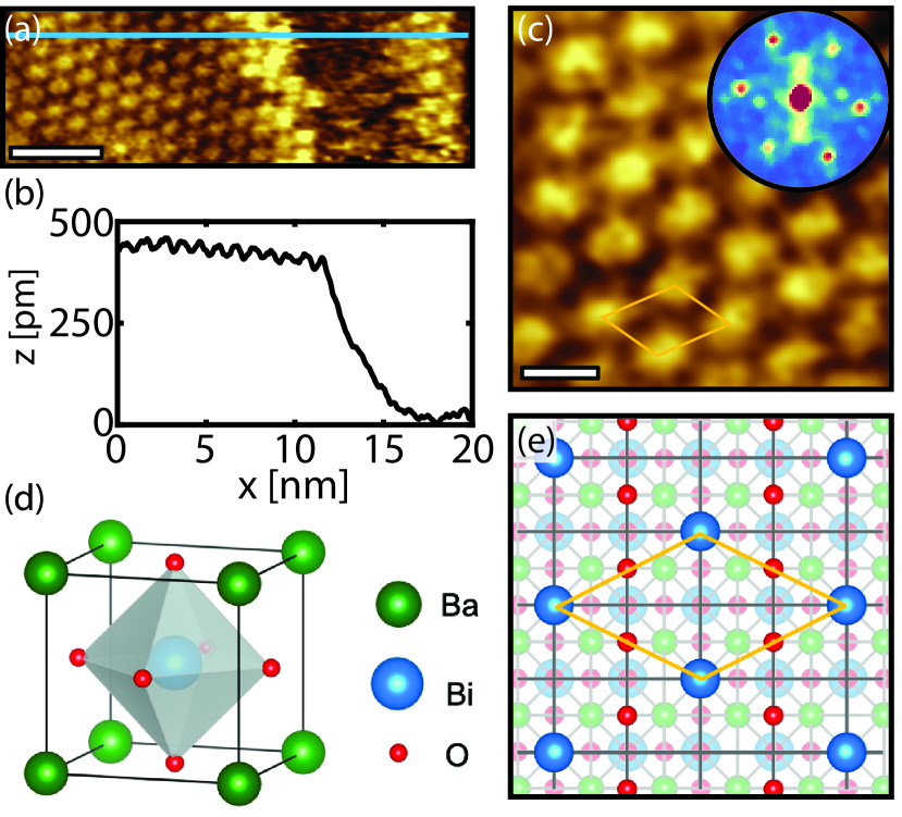
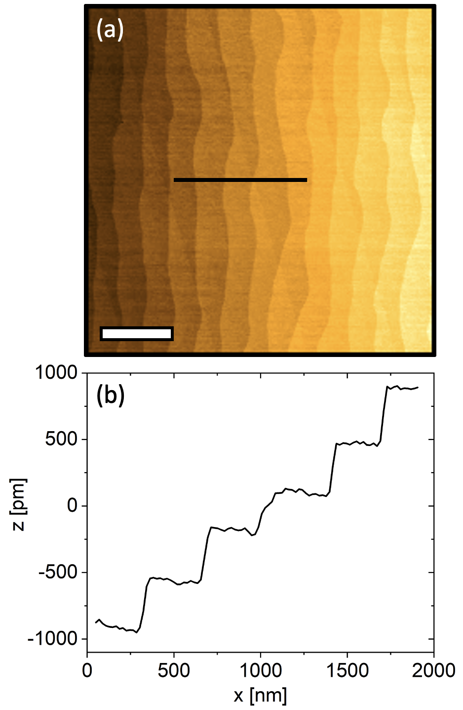
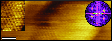
Fig. 1(a) shows the surface of the 10-unit-cell-thick BBO film on Nb:STO. The corresponding height profile across the surface is presented in Fig. 1(b) and reveals a step height of approximately 4.5 Å. This is consistent with a single unit cell of BBO (a = 4.35 Å) [29]. Fig. 1(c) shows a zoomed image of the BBO surface. The observed pattern of atoms corresponds to a c(4 2) surface reconstruction, the diamond-shaped orange lines indicate its unit cell. The same surface reconstruction is also found for the 4-unit-cell-thick BBO film, shown in the Supplementary Material. In Fig. 1(e) the surface reconstruction on the BBO surface is schematically depicted, the orange diamond-shaped lines indicate the unit cell and correspond to the orange lines in Fig. 1(c).
Erdman et. al [33] concluded for the c(4 2) reconstruction on a STO(001) surface that a stoichiometric TiO2 overlayer was present, consisting of TiO5 edge-sharing polyhedra. Such an overlayer is formed to stabilize the truncated, corner-sharing octahedra in the surface layer of a TiO2-terminated STO(001) underneath. Therefore, we propose, in analogy with the studies on Nb:STO(001) and STO(001), that a BiO2 overlayer is present on the surface of BBO, hosting BiO5 edge-sharing polyhedra.
The Fast Fourier transform (FFT), shown in the inset of Fig. 1(c), has a threefold symmetry with a periodicity of 1 nm. Note that the underlying crystal structure is still a fourfold symmetric cubic perovskite structure. The lattice constant corresponding to a periodicty of 1 nm is 4.35 Å ( 4.35 Å = 1 nm), which is in agreement with the BBO lattice constant. The surface reconstruction on the 4-unit-cell-thick BBO film also has a periodicity of 1 nm, as presented in the Supplementary Material. Previous studies on Nb:STO(001) and STO(001) surfaces revealed the same type of reconstruction, however, with a periodicity of 0.88 nm – corresponding to a bulk lattice constant of 3.9 Å [33, 34, 35] matching STO (a = 3.905 Å) [36].
The observation of BBO thin films with a relaxed lattice constant is in good agreement with our previous study [29], where we show – by means of a scanning transmission electron microscopy (STEM) – that a lattice mismatch of 12% between the STO substrate and BBO film is accommodated by the formation of an interfacial layer. This was confirmed by Jin et al. [37], where an interfacial layer with a fluorite structure and similar thickness is observed at the STO/BBO interface. The interfacial layer decouples the BBO film from the substrate. The bottommost part is still strained to the STO substrate, but the subsequent layer is already fully decoupled and relieves all strain in a dislocation every ninth unit cell [29]. Therefore, the substrate does not influence the BBO film.
The BBO film is able to continue its growth without any effects of strain in a perovskite structure [29, 37]. Anti-phase boundaries, where a step of half a unit cell is present, are observed within the BBO film in various STEM studies [28, 29, 37]. However, this boundary does not disturb the quality of the film. The suggested suppression of the oxygen breathing mode as a function of thickness has not yet been observed by STEM. The structural transition from tetragonal to cubic, as previously observed [25], is too small to be detected by STEM since it occurs on the picometer range.
The presence of the surface reconstruction, with an identical periodicity for the 4- and 10-unit-cell-thick BBO films, proves that the underlying structure in both cases is still the perovskite structure with the relaxed lattice constant of bulk BBO. The subsequently presented spatially-resolved STS measurements are, therefore, observing the effect of thickness and not of substrate-induced strain nor defects.
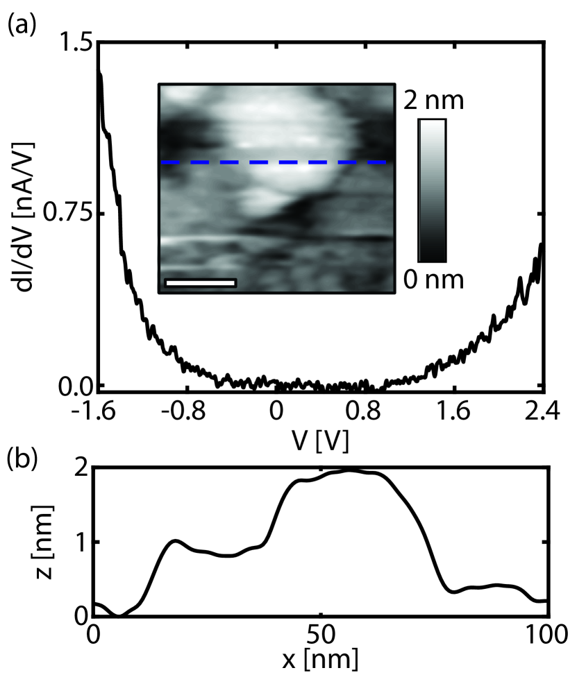
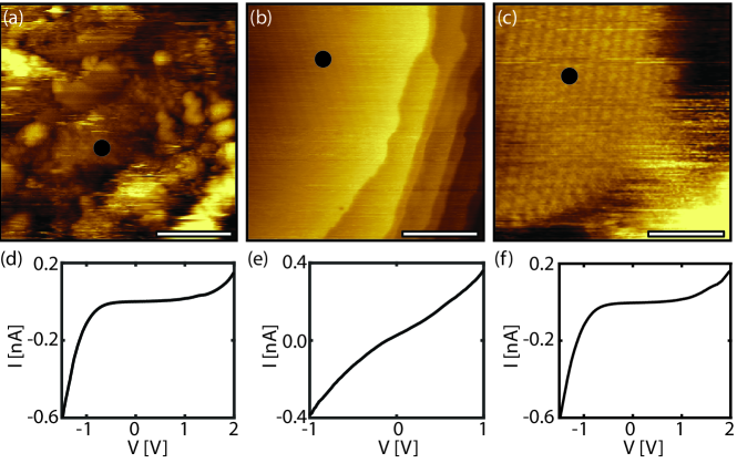
STS was first used to determine the electronic properties of the 16-unit-cell-thick BBO film. In Fig. 2(a), the differential conductance curves () represent the local density of states (LDOS). A semiconducting characteristic with a band gap () of 1.2 0.3 eV is observed. From the cross-section height profile (see Fig. 2(b)) variations of 2 nm are observed, which have no clear spatial-dependent influence on the electronic profile across the surface. The band gap is asymmetric with the valence band located closer to the Fermi level ().
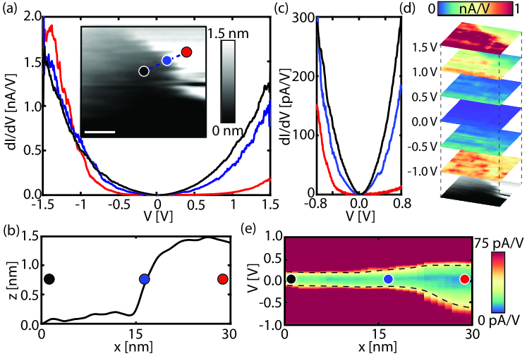
In the case of the 10-unit-cell-thick BBO film, the LDOS varies spatially. Fig 3(a) shows the LDOS on various locations on the sample, the colored dots on the topography image in the inset correspond to colors of the differential conductance spectra. On the thicker part of the sample, represented by the red curve in Fig. 3(a), semiconducting behavior is observed – similar to the profile on the 16-unit-cell-thick BBO film in Fig. 2(a). However, the size of the band gap is reduced to 0.7 0.2 eV.
From the cross-section height profile, see Fig. 3(b), it is clear that the lower region (black dot) is located 1.4 nm ( 3 u.c.) lower with respect to the higher region (red dot). Note that the exact thickness of the BBO film is unknown and therefore only relative thicknesses are given. The spectra taken at the lower region of the sample, black curve in Fig. 3(a), reveal a significant reduction of . A closer look at the Fermi energy, depicted in Fig. 3(c), shows this even more clearly. The band gap reduces to approximately 0.10 0.03 eV.
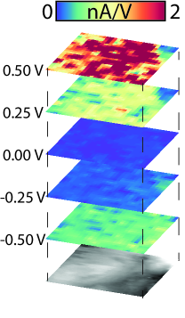
The simultaneously obtained differential conductance (d/d) maps, presented in Fig. 3(d), depict the LDOS for the thickness regions at different bias voltages. A clear correlation is observed between the topography, bottommost image, and the LDOS. At non-zero bias voltages, the LDOS is much higher at the lower region of the sample compared to the higher region. At zero bias voltage all the contrast is lost and the regions can no longer be distinguished, excluding the presence of a metallic state.
In between the two height regions, a transition region is present, indicated by the blue dot in the inset of Fig. 3(a) and by the blue curve in (a) and (c). The size of the band gap depends heavily on the exact location on the sample, this is better visualized in Fig. 3(e). The measured curves are plotted as a function of the distance, the colored dots correspond to the dots in the inset of Fig. 3(a). A continuous but steep transition in the band gap size is found between the two regions.
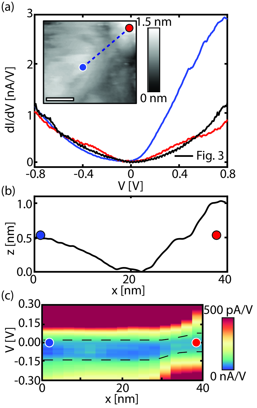
To further confirm the observed band gap reduction, the 4-unit-cell-thick BBO film is studied. Fig. 4(a) shows the location-dependent differential conductance. The LDOS measured on the higher region of the 4 u.c. BBO film (red curve in Fig. 4(a)) has the same characteristics as the spectrum measured on the lower region of the 10 u.c. BBO film (black curve in Fig. 3(a) and (c)), including a similar band gap of 0.10 0.05 eV. For better visualization, the scaled differential conductance spectrum of Fig. 3(c) (black curve) is also plotted in Fig. 4(a).
On the region located 1 u.c. lower, see the height profile in Fig. 4(b), the LDOS is altered again (blue curve in Fig. 4(a)). In addition to a small decrease in the size of the band gap (i.e. 0.07 0.04 eV), the band gap is no longer positioned symmetrically relative to the Fermi energy. A small shift towards negative voltages is observed (i.e. the conductance band is located closer to ), which is most likely caused by band bending. The contact potential difference between Nb:STO and BBO results in an accumulation layer of electrons in the BBO film, bending the conduction band towards the Fermi energy. Fig. 4(c) shows the as a function of the distance. The shift of the band gap towards more negative voltages at the lower region (blue dot) is clearly observed.
From the BBO thin film thickness series, we observed the following: 1) a reduction of the band gap as a function of decreasing thickness, 2) the absence of a metallic state and 3) a monotonous but steep transition in the band gap size between the different thickness regions. Although an insulator-to-metal transition was predicted [25], a clear wide-gap ( 1.2 eV) to small-gap ( 0.07 eV) semiconductor transition is observed as a function of .
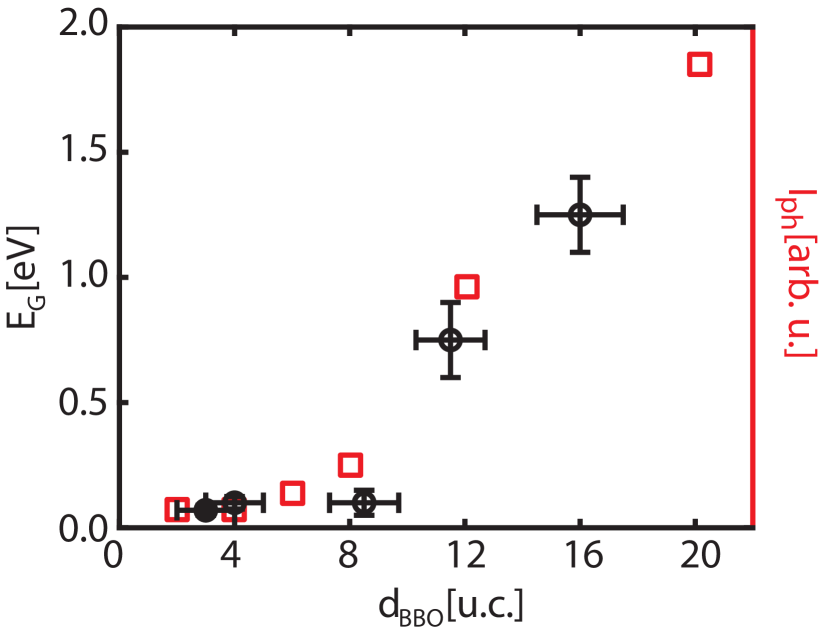
In Fig. 5, the determined band gap sizes are plotted as a function of thickness. The uncertainty in thickness for the BBO films is determined from atomic force microscopy (AFM) images, presented in the Supplementary Material. The transition from a wide-gap to a small-gap semiconductor is continuous and gradual. Recent density functional theory (DFT) calculations in combination with a tight-binding (TB) model [21] revealed the influence of the oxygen breathing mode on the band structure of BBO. If the oxygen breathing mode is absent, a metallic band structure is predicted, while a band gap forms when the oxygen breathing mode is present. Implying that a semiconductor-metal transition occurs when the oxygen breathing mode is suppressed, as we observe as a function of thickness. No metallicity is observed, even for the 4-unit-cell-thick BBO film, implying that the oxygen breathing mode is not fully suppressed.
On the right axis of Fig. 5, the intensity of the Raman response of the breathing phonon mode () is plotted (data from ref. [27]). A coinciding dependence between and as a function of the BBO film thickness is observed. Synchrotron XRD and Raman spectroscopy experiments suggest that the strength of the oxygen breathing mode is decreasing with thickness [25, 26, 27]. Therefore, we conclude that the closing of the band gap originates from the suppression of the oxygen breathing mode as a function of thickness.
For increasing thickness, around a thickness of 8 u.c., both the band gap size and the intensity of the breathing phonon intensity start to increase. In both cases, the BBO films remain insulating up to the ultra-thin limit of 3 u.c. In addition, no step-like suppression in the breathing phonon intensity or the band gap is observed, in good agreement with previous studies [25, 26, 27]. The observed c(4 2) surface reconstruction on the BBO films with thicknesses of 4 and 10 u.c., confirms the underlying structure is the perovskite structure and not an interfacial layer [29, 37] and the identical periodicity proves that no substrate-induced strain effect is present.
The influence of the breathing phonon mode on the band gap also explains the discrepancy between the observed band gap of the 16-unit-cell-thick BBO film (shown in Fig. 2) and the optical determined band gap on BBO (1.2 eV versus 2.0 eV) in previous studies (for single crystals [10, 11] and for films with 300 nm [12]). This discrepancy is a consequence of the thickness-dependent band gap variation. In refs. [25, 27], it is clearly shown that the BBO breathing phonon intensity was already affected for BBO thicknesses of 30 u.c. Therefore, the band gap on the 16-unit-cell-thick BBO film is already reduced and not reaching the optically measured 2 eV band gap.
In conclusion, by combining STM and STS, we observed a thickness-dependent wide-gap to small-gap semiconductor transition in BBO thin films. For 16 u.c., a band gap of 1.2 0.3 eV is observed. With a reduction of the film thickness, the band gap shrinks to approximately 0.07 0.04 eV for a 3-unit-cell-thick BBO film. No metallic state was detected in the ultra-thin limit. The transition is continuous and gradual and shows a coinciding dependence with the intensity of the Raman response of the breathing phonon mode as a function of thickness. A c(4 2) surface reconstruction is observed on the 4- and 10-unit-cell-thick BBO films, confirming the perovskite structure with the correct lattice constant underneath, excluding the influence of substrate-induced strain. The presented results show that the suppression of the oxygen breathing mode as a function of thickness is responsible for the modification of the band gap size.
The authors thank Dominic Post and Martin Siekman for technical support and Prof. Dr. Ir. Harold J.W. Zandvliet for fruitful discussions.
I
II Supplementary Material:
Thickness-Dependent Band Gap Modification in BaBiO3
III Sample fabrication and characterization
As a substrate Nb-doped SrTiO3(001) (Nb:STO) (from CrysTec GmbH) was used, with a doping level of 0.5 wt%. To obtain a TiO2 single-terminated surface, a wet etching step of 30 seconds in a buffered hydrogen fluoride solution was performed [38]. Subsequently, the substrates were annealed for 1.5 hours in a furnace with a continuous oxygen flow at 930 ∘C. Afterwards, the surface quality was checked with an atomic force microscope (AFM). A 4 4 m image of a Nb:STO is presented in Fig. S1(a), nicely arranged terraces are observed. The height profile, see Fig. S1(b) and corresponding to the black line in (a), shows straight terraces with a step height of approximately 0.4 nm – in good agreement with the STO bulk lattice constant of 3.905 Å [36].
The BaBiO3 thin films were fabricated using pulsed laser deposition (PLD). Before each deposition, the target was sanded and a pre-ablation was performed with 600 pulses fired at 5 Hz in the same oxygen background pressure as used during the actual deposition. The same growth conditions were used as in [29]: a KrF laser at a fluence of 1.9 J/cm2 with a repetition rate of 1 Hz, substrate temperature of 500 ∘C, oxygen background pressure of 0.0100 mbar and a substrate-target distance of 50 mm.
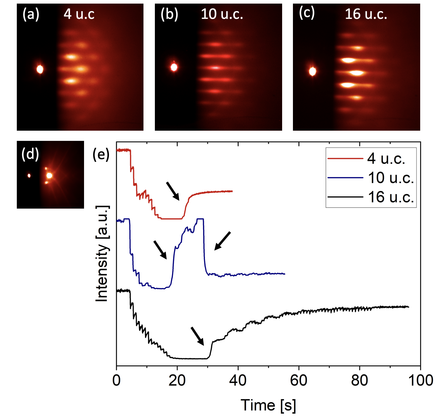
During the deposition, the growth of the BBO films was monitored by reflection high-energy electron diffraction (RHEED). In Fig. S2(a-c) the RHEED patterns of the BBO films with thicknesses 4, 10 and 16 unit cells (u.c.), respectively, are presented. The images are taken after cool down in high vacuum conditions (average pressure of 3 x 10⁻⁷ mbar). In Fig. S2(d) the diffraction pattern of the Nb:STO substrate, used for the 4-unit-cell-thick BBO film, is shown. In Fig. S2(e), the intensity of the main diffraction spot, that was monitored during growth, is presented as function of time. The red, blue and black curve correspond with the 4-, 10- and 16-unit-cell-thick BBO films, respectively. The small black arrows indicate where the intensity is manually de- or increased.
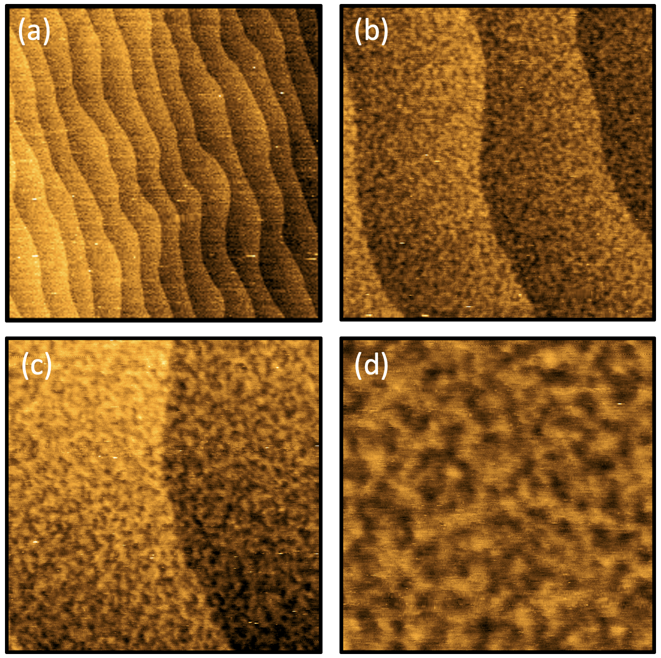
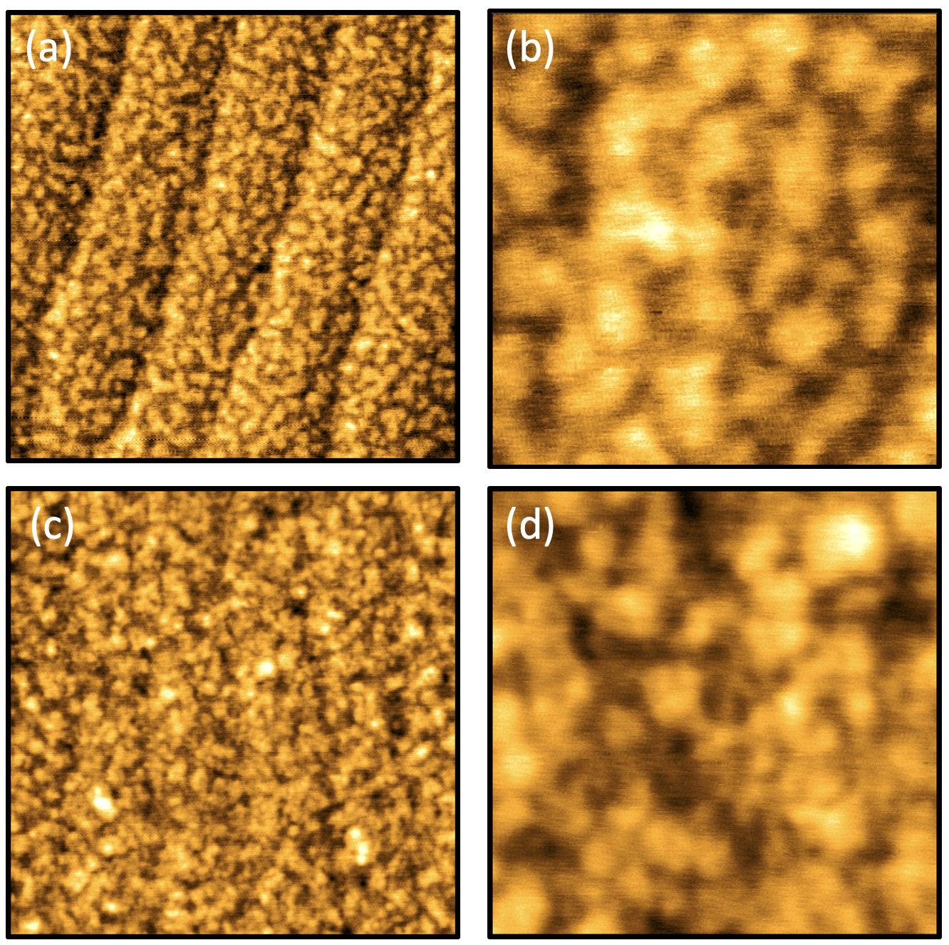
The three BBO films were in-situ transferred to a Nanoprobe scanning tunneling microscope (STM) for spectroscopy experiments. A 4-unit-cell-thick BBO film was removed from the vacuum and directly studied with an AFM, the result is presented in Fig. S3. The substrate terraces are still visible, but when scanning a smaller area (the area decreases going from (a) to (d)) some roughness is observed. The root-mean-square (RMS) roughness is 150 20 pm.
The same is performed for a 10- and a 16-unit-cell-thick BBO film (see Fig. S4), the AFM images are presented in (a, b) and (c, d), respectively. The average RMS roughnesses are 200 20 pm and 350 20 pm for the 10 and 16 u.c. BBO films, respectively. The RMS values are used as a measure for the x-axis error bars in Fig. 5 of the main text.
IV Scanning tunneling microscopy
The results of the spectroscopy experiments with the 4-, 10- and 16-unit-cell-thick BBO films are presented in the main text. Below, some additional results are presented.
IV.1 Surface reconstruction of a 4-unit-cell-thick film
Fig. S5 shows the surface of the 4-unit-cell-thick BBO film on Nb:STO. The image is slightly distorted due the presence of a double tip. The atoms are arranged in the same symmetry and periodicity as for the 10-unit-cell-thick BBO films (Fig. 1 of the main text), corresponding to a c(4 2) surface reconstruction.
IV.2 LDOS 4 u.c. BBO film
In Fig. S6 the spatially resolved local density of states (LDOS) for the 4-unit-cell-thick BBO film is shown for different bias voltages. Around the Fermi energy, no contrast is observed, similar as for the 10-unit-cell-thick BBO film (see Fig. 3(d) in the main text). Only for V, clear correlations are observed between the LDOS maps and the topography (bottom most image, same as inset of Fig. 4(a) in the main text). The higher region (see red dot in the inset of Fig. 4(a) in the main text) has a significantly lower LDOS than the lower region (blue dot).
IV.3 Band gap determination
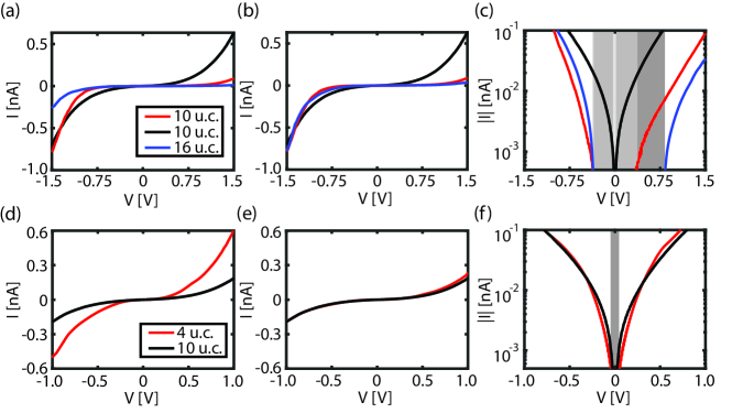
In order to properly compare the band gap measured on the different samples, the curves are first scaled to the same set point. In Fig. S7(a-c) the 10- and 16-unit-cell-thick BBO films are compared. Since it was not possible to use the same scan settings on both surfaces, the spectrum of the 16 u.c. BBO film is scaled to the set point used for the curves obtained on the 10 u.c. BBO film ( = 600 pA and = -1.5 V, Fig. S7(b)). The size of the band gap () is determined for all measurements by plotting the corrected spectra on a semi-logarithmic scale (see Fig. S7) and, subsequently, taking the average voltage separation between the conduction band and valence band current onsets at the lowest detectable current (detection limit approximately 500 fA) [30, 31, 32].
From this measure a difference in the band gap is obtained between the 10 and 16 u.c. BBO films (see Fig. S7(c)). A similar approach is used to compare the 4 and 10 u.c. BBO samples, presented in Fig. S7(d-f). The obtained curve on the 10-unit-cell-thick BBO film is scaled with respect to the curve measure on the 4-unit-cell thick BBO film ( = 400 pA and = 1 V). Although the absolute value for the band gap extracted from STS spectra depends slightly on the chosen scan parameters, the increasing trend between the thickness and the size of the band gap (Fig. 5 in the main text) remains unaffected.
IV.4 Topography and spectroscopy
Some of the topography images look a little bit scratchy, even though the measurements are repeatedly performed with different tips and scanners (the measurements are performed in the Nanoprobe STM which contains four indepently operating scanners). In order to exclude the possibility that the tips are contaminated, topography and spectroscopy data is presented in Fig. S8, taken before and after scanning on Au(111).
In Fig. S8(a), a topography scan on a 10-unit-cell-thick BBO sample is presented. The topography looks a bit scratchy, but terraces are still visible. The measured curve is displayed in Fig. S8(d) and shows the presence of a band gap. After the measurement on the BBO film, the sample was replaced by Au(111) (see Fig. S8(b)). Several steps are visible and on the terrace the herringbone reconstruction is present [39], indicating that the quality of the tip is good. Also, a metallic spectrum is measured in the measurement, presented in Fig. S8(e).
Subsequently, the 10-unit-cell-thick BBO film is scanned. A higher quality topography scan is obtained, see Fig. S8(c), with a similar spectroscopy measurement (Fig. S8(f)) as initially observed on BBO (Fig. S8(d)). Although the same tip and tunneling parameters are used, the image quality is slightly improved implicating that the scratchy topography appearance is not caused by the tip quality but reflects the state of the surface. Furthermore, the topography image of Fig. S8(a) (and also of Fig. 3 and 4 of the main text) look very similar to the topography images scanned with the AFM in Fig. S3 and Fig. S4, suggesting that it is a not a tip artifact that is measured.
References
- Scholder et al. [1963] R. Scholder, K. W. Ganter, H. Gläser, and G. Merz, Über Alkali- und Erdalkalioxobismutate(V), Zeitschrift für anorganische und allgemeine Chemie 319, 375 (1963).
- Ge et al. [2018] J. Ge, W.-J. Yin, and Y. Yan, Solution-Processed Nb-Substituted BaBiO3 Double Perovskite Thin Films for Photoelectrochemical Water Reduction, Chemistry of Materials, Chemistry of Materials 30, 1017 (2018).
- Chouhan et al. [2018] A. S. Chouhan, E. Athresh, R. Ranjan, S. Raghavan, and S. Avasthi, BaBiO3: A potential absorber for all-oxide photovoltaics, Materials Letters 210, 218 (2018).
- Pei et al. [1990] S. Pei, J. D. Jorgensen, B. Dabrowski, D. G. Hinks, D. R. Richards, A. W. Mitchell, J. M. Newsam, S. K. Sinha, D. Vaknin, and A. J. Jacobson, Structural phase diagram of the system, Phys. Rev. B 41, 4126 (1990).
- Baumert [1995] B. A. Baumert, Barium potassium bismuth oxide: A review, Journal of Superconductivity 8, 175 (1995).
- A. W. Sleight and J. L. Gillson and P. E. Bierstedt [1975] A. W. Sleight and J. L. Gillson and P. E. Bierstedt, High-temperature superconductivity in the BaPb1-xBixO3 systems, Solid State Communications 17, 27 (1975).
- Cox and Sleight [1976] D. E. Cox and A. W. Sleight, Crystal structure of Ba2Bi3+Bi5+O6, Solid State Communications 19, 969 (1976).
- Tajima et al. [1985] S. Tajima, S. Uchida, A. Masaki, H. Takagi, K. Kitazawa, S. Tanaka, and A. Katsui, Optical study of the metal-semiconductor transition in BaPb1-xBixO3, Phys. Rev. B 32, 6302 (1985).
- Wertheim et al. [1982] G. K. Wertheim, J. P. Remeika, and D. N. E. Buchanan, Electronic structure of BaPb1-xBixO3, Phys. Rev. B 26, 2120 (1982).
- Lobo and Gervais [1995] R. P. S. M. Lobo and F. Gervais, Bismuth disproportionation in BaBiO3 studied by infrared and visible reflectance spectra, Phys. Rev. B 52, 13294 (1995).
- Tajima et al. [1987] S. Tajima, S. Uchida, A. Masaki, H. Takagi, K. Kitazawa, S. Tanaka, and S. Sugai, Electronic states of BaPb1-xBixO3 in the semiconducting phase investigated by optical measurements, Phys. Rev. B 35, 696 (1987).
- Sato et al. [1989] H. Sato, S. Tajima, H. Takagi, and S. Uchida, Optical study of the metal-insulator transition on Ba1-xKxBi03 thin films, Nature 338, 241 (1989).
- Mattheiss et al. [1988] L. F. Mattheiss, E. M. Gyorgy, and D. W. Johnson, Superconductivity above 20 K in the Ba-K-Bi-O system, Phys. Rev. B 37, 3745 (1988).
- Cava et al. [1988] R. J. Cava, B. Batlogg, J. J. Krajewski, R. Farrow, L. W. Rupp, A. E. White, K. Short, W. F. Peck, and T. Kometani, Superconductivity near 30 K without copper: the Ba0.6K0.4BiO3 perovskite, Nature 332, 814 (1988).
- Cox and Sleight [1979] D. E. Cox and A. W. Sleight, Mixed-valent Ba2Bi3+Bi5+O6: structure and properties vs temperature, Acta Crystallographica Section B 35, 1 (1979).
- Franchini et al. [2010] C. Franchini, A. Sanna, M. Marsman, and G. Kresse, Structural, vibrational, and quasiparticle properties of the Peierls semiconductor BaBiO3: A hybrid functional and self-consistent GW + vertex-corrections study, Phys. Rev. B 81, 085213 (2010).
- Mattheiss and Hamann [1982] L. F. Mattheiss and D. R. Hamann, Electronic- and crystal-structure effects on superconductivity in the BaPb1-xBixO3 system, Phys. Rev. B 26, 2686 (1982).
- Mattheiss and Hamann [1983] L. F. Mattheiss and D. R. Hamann, Electronic structure of BaPb1-xBixO3, Phys. Rev. B 28, 4227 (1983).
- Korotin, Dm. and Kukolev, V. and Kozhevnikov, A. V. and Novoselov, D. and Anisimov, V. I. [2012] Korotin, Dm. and Kukolev, V. and Kozhevnikov, A. V. and Novoselov, D. and Anisimov, V. I., Electronic correlations and crystal structure distortions in BaBiO3, Journal of Physics: Condensed Matter 24, 415603 (2012).
- Foyevtsova et al. [2015] K. Foyevtsova, A. Khazraie, I. Elfimov, and G. A. Sawatzky, Hybridization effects and bond disproportionation in the bismuth perovskites, Phys. Rev. B 91, 121114(R) (2015).
- Khazraie et al. [2018] A. Khazraie, K. Foyevtsova, I. Elfimov, and G. A. Sawatzky, Oxygen holes and hybridization in the bismuthates, Phys. Rev. B 97, 075103 (2018).
- Dalpian et al. [2018] G. M. Dalpian, Q. Liu, J. Varignon, M. Bibes, and A. Zunger, Bond disproportionation, charge self-regulation, and ligand holes in and in -electron perovskites by density functional theory, Phys. Rev. B 98, 075135 (2018).
- Balandeh et al. [2017] S. Balandeh, R. J. Green, K. Foyevtsova, S. Chi, O. Foyevtsov, F. Li, and G. A. Sawatzky, Experimental and theoretical study of the electronic structure of single-crystal , Phys. Rev. B 96, 165127 (2017).
- Plumb, N. C. and Gawryluk, D. J. and Wang, Y. and Ristić, Z. and Park, J. and Lv, B. Q. and Wang, Z. and Matt, C. E. and Xu, N. and Shang, T. and Conder, K. and Mesot, J. and Johnston, S. and Shi, M. and Radović, M. [2016] Plumb, N. C. and Gawryluk, D. J. and Wang, Y. and Ristić, Z. and Park, J. and Lv, B. Q. and Wang, Z. and Matt, C. E. and Xu, N. and Shang, T. and Conder, K. and Mesot, J. and Johnston, S. and Shi, M. and Radović, M., Momentum-Resolved Electronic Structure of the High-Tc Superconductor Parent Compound BaBiO3, Phys. Rev. Lett. 117, 037002 (2016).
- Kim et al. [2015] G. Kim, M. Neumann, M. Kim, M. Le, T. Kang, and T. Noh, Suppression of three-dimensional charge density wave ordering via thickness control, Phys. Rev. Lett. 115, 226402 (2015).
- Lee et al. [2018] H. G. Lee, R. Kim, J. Kim, M. Kim, T. H. Kim, S. Lee, and T. W. Noh, Anisotropic suppression of octahedral breathing distortion with the fully strained BaBiO3/BaCeO3 heterointerface, APL Materials 6, 016107 (2018).
- Zapf et al. [2019] M. Zapf, S. Elsässer, M. Stübinger, P. Scheiderer, J. Geurts, M. Sing, and R. Claessen, Structural and stoichiometric modifications in ultrathin epitaxial BaBiO3 films, Phys. Rev. B 99, 245308 (2019).
- Zapf et al. [2018] M. Zapf, M. Stübinger, M. Kamp, F. Pfaff, A. Lubk, B. Büchner, M. Sing, and R. Claessen, Domain matching epitaxy of BaBiO3 on SrTiO3 with structurally modified interface, Appl. Phys. Lett. 112, 141601 (2018).
- Bouwmeester et al. [2019] R. L. Bouwmeester, K. de Hond, N. Gauquelin, J. Verbeeck, G. Koster, and A. Brinkman, Stabilization of the perovskite phase in the Y–Bi–O system by using a BaBiO3 buffer layer, Phys. Status Solidi RRL 13, 1800679 (2019).
- Feenstra and Stroscio [1987] R. Feenstra and J. Stroscio, Tunneling spectroscopy of the gaas(110) surface, J. Vac. Sci. Technol. B 5, 923 (1987).
- Ebert et al. [2011] P. Ebert, S. Schaafhausen, A. Lenz, A. Sabitova, L. Ivanova, M. Dahne, Y. L. Hong, S. Gwo, and H. Eisele, Direct measurement of the band gap and Fermi level position at InN(1120), Appl. Phys. Lett. 98 (2011).
- Herbert et al. [2013] F. W. Herbert, A. Krishnamoorthy, K. J. van Vliet, and B. Yildiz, Quantification of electronic band gap and surface states on FeS2(100), Surf. Sci. 618, 53 (2013).
- Erdman et al. [2003] N. Erdman, O. Warschkow, M. Asta, K. R. Poeppelmeier, D. E. Ellis, and L. D. Marks, Surface Structures of SrTiO3(001): A TiO2-rich Reconstruction with a c(4x2) Unit Cell, J. Am. Chem. Soc. 125, 10050 (2003).
- Jiang and Zegenhagen [1999] Q. D. Jiang and J. Zegenhagen, c(6×2) and c(4×2) reconstruction of SrTiO3(001), Surf. Sci. 425, 343 (1999).
- Castell [2002] M. R. Castell, Scanning tunneling microscopy of reconstructions on the SrTiO3(001) surface, Surf. Sci. 505, 1 (2002).
- Ohtomo and Hwang [2004] A. Ohtomo and H. Y. Hwang, A high-mobility electron gas at the LaTiO3/SrTiO3 heterointerface, Nature 427, 423 (2004).
- Jin et al. [2020] L. Jin, M. Zapf, M. Stübinger, M. Kamp, M. Sing, R. Claessen, and C. L. Jia, Atomic‐Scale Interface Structure in Domain Matching Epitaxial BaBiO3 Thin Films Grown on SrTiO3 Substrates, Phys. Status Solidi RRL 14, 2000054 (2020).
- Koster et al. [1998] G. Koster, B. L. Kropman, G. J. H. M. Rijnders, D. H. A. Blank, and H. Rogalla, Quasi-ideal strontium titanate crystal surfaces through formation of strontium hydroxide, Applied Physics Letters 73, 2920 (1998).
- Wöll et al. [1989] C. Wöll, S. Chiang, R. Wilson, and L. P.H., Determination of atom positions at stacking-fault dislocations on au(111), Phys. Rev. B 39, 7988 (1989).