Competing correlated states around the zero field Wigner crystallization transition of electrons in two-dimensions
Abstract
The competition between kinetic energy and Coulomb interactions in electronic systems can lead to complex many-body ground states with competing superconducting, charge density wave, and magnetic orders. Here we study the low temperature phases of a strongly interacting zinc-oxide-based high mobility two dimensional electron system that displays a tunable metal-insulator transition. Through a comprehensive analysis of the dependence of electronic transport on temperature, carrier density, in-plane and perpendicular magnetic fields, and voltage bias, we provide evidence for the existence of competing correlated metallic and insulating states with varying degrees of spin polarization. Our system features an unprecedented level of agreement with the state-of-the-art Quantum Monte Carlo phase diagram of the ideal jellium model, including a Wigner crystallization transition at a value of the interaction parameter and the absence of a pure Stoner transition. In-plane field dependence of transport reveals a new low temperature state with partial spin polarization separating the spin unpolarized metal and the Wigner crystal, which we examine against possible theoretical scenarios such as an anti-ferromagnetic crystal, Coulomb induced micro-emulsions, and disorder driven puddle formation.
Dilute interacting electrons harbor competing ground states when their Coulomb repulsion greatly exceeds their kinetic energy. In a parabolically dispersing two dimensional electron system (2DES) the ratio of interaction to kinetic energy scales is parameterized by the dimensionless parameter , given by
| (1) |
Here, is the effective Bohr radius of carriers and is the electron concentration. As the density is lowered, the electron system undergoes a Wigner crystallization transition, which Quantum Monte Carlo (QMC) studies predict to occur at around [Tanatar and Ceperley, 1989; Rapisarda and Senatore, 1996; Phillips et al., 1998; Chamon et al., 2001; Attaccalite et al., 2002; Spivak and Kivelson, 2004; Drummond and Needs, 2009]. In spite of decades of research efforts,Spivak et al. (2010); Abrahams et al. (2001); Kravchenko and Sarachik (2003); Shashkin and Kravchenko (2019); Dolgopolov (2019) many aspects of the phase diagram of a strongly interacting 2DES in the limit of zero temperature and zero magnetic field remain clouded in the range of , where QMC calculations predict a breakdown of the Fermi liquid (FL) state. One of the main obstacles has been the trade-off of interaction and disorder strengths in these platforms; namely, the cleanest systems, such as electron-doped GaAs, are also typically the ones that are relatively weakly interacting, while those with stronger interactions tend to be more disordered. Thus, systematic experimental studies in the high regime () remain few.Yoon et al. (1999); Knighton et al. (2018); Hossain et al. (2020) The advent of ZnO heterostructures, however, offers a new platform that is sufficiently strongly interacting and clean. This combination is evidenced by its display of some of the most fragile correlated states of the fractional quantum Hall regime, such as the 5/2 and 7/2 incompressible states, bubbles and stripes,Falson et al. (2015, 2018) while still remaining strongly interacting at zero magnetic field, as we demonstrate in this study.
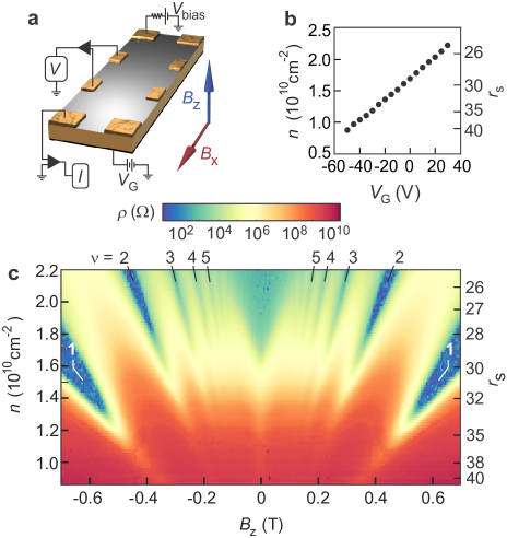
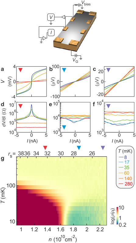
The enhanced electronic interactions in MgZnO/ZnO heterostructures stem primarily from the relatively heavy band mass () and small dielectric constant (). Moreover, the occupation of a single electron pocket at combined with weak non-parabolicity and spin-orbit interaction ensure that the system is very close to the ideal jellium model studied in QMC. The bands are highly spin degenerate, and the band -factor () is isotropic.Kozuka et al. (2013) The quasi-Hall bar device under study is rendered in Fig.1a. The epitaxial MgZnO/ZnO heterostructure confines a 2DES approximately 500 nm beneath the wafer surface with tuned in-situ via a capacitively coupled gate electrode on the back-side of the wafer. The field-effect transfer characteristics are displayed in Fig.1b. Here, is determined from the period of quantum oscillations and Hall effect. Great effort has been invested to perform experiments at very low temperatures, as many transport features are revealed only below mK. To this end, the sample is immersed within a liquid 3He bath in a cryostat that operates down to mK. The electrical characteristics are probed in a four-point configuration by sweeping the DC bias () applied while measuring the current across the device () and local longitudinal voltage drop (), yielding a single trace. The first derivative of this data provides the differential resistance () of the device as a function of . We define to be in the small current limit ( nA), which probes the linear response of the equilibrium state of the system.
The magnetotransport of the device in the (,) parameter space is presented in Fig. 1c. Oscillatory features in as is increased are associated with integer steps in Landau quantization. These states are labeled according to their filling factor , where is the Planck constant and is the elementary charge. Low-field oscillations begin at approximately 0.07 T, yielding a conservative estimate of the quantum lifetime of carriers 10 ps, using the relationship where is the cyclotron frequency at the onset of oscillations and the band mass.
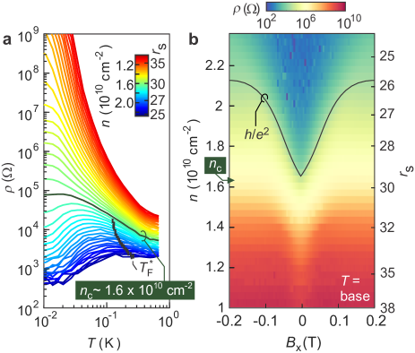
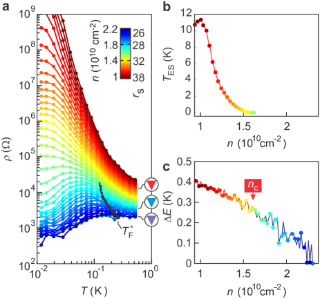
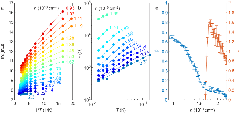
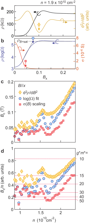
The data in Fig. 2a presents of the device at zero magnetic field. This data reveals a crossover from a metallic to insulating dependence at a critical density 1010 cm-2 (corresponding to ), enabling us to associate the density with a zero-field metal-insulator transition (MIT) close to the quantum resistance value . Data for mK deviates from the systematic behavior at higher temperatures, most likely due to the commonly encountered issue of decoupling of the electron temperature from that of the immersion cryogen. The effect of an in-plane magnetic field is displayed in Fig.2b, which indicates a positive magnetoresistance at all values of the electron density. The value is identified as a black line, which corresponds to a finite when is slightly larger than .
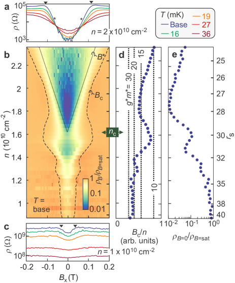
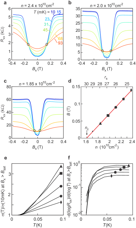
The in-plane magnetic field permits us to directly control the degree of spin polarization of the electrons, as the orbital coupling to in-plane fields is negligible due to the two-dimensional confinement. Figure 3a plots the magnetoresistance of the device as a function of at 1010 cm-2and at various temperatures. From these curves we can identify two values of the magnetic field of interest: , at which saturates to a value of (black triangle); and , at which there is a change in the sign of from metallic-like to insulating-like. can be interpreted as the critical field required to reach full spin polarization.Spivak et al. (2010); Abrahams et al. (2001); Kravchenko and Sarachik (2003); Shashkin and Kravchenko (2019); Dolgopolov (2019) Figure 3b plots the ratio in the (,)-plane, with orange regions associated with a fully spin polarized 2DES. The data in Fig. 3 reveals a non-monotonic dependence of as a function of (dashed line) as the MIT is crossed. We observe an inflection point in the value of around 1010 cm-2, which is higher than the the value associated with the zero field MIT. The in-plane field traces reveal the presence of finite magnetoresistance even in the low-density limit (Fig. 3c), where the device is insulating for all .
The dotted line in Fig. 3b marks the value of at which the sign of the temperature dependence of resistivity changes, from metallic-like (low ) to insulating-like (high ). Thus, the (,) parameter space hosts two regions with an insulating-like temperature dependence , namely at when , and at all when . As we show in the SI (Sec. S7), in the latter regime of the temperature dependence is consistent with the activated or VRH mechanisms that are characteristic of insulators Shklovskii and Efros (1984) (including Wigner crystalsShklovskii (2004)). In contrast, in the regime of and where we encounter what appears as a field-induced MIT, the dependence of resistivity on temperature is more consistent with a linear or power-law relation. Such a linear increase in with , and the accompanying change in sign of , has been shown theoretically to arise in metallic, correlated states with high spin polarization Zala et al. (2001a, b). Thus, the temperature dependence points to a ground state at and that is distinct from the low-density insulating phase for at .
The value of allows us to measure the renormalized spin susceptibility of the system, . Experimentally, it is convenient to use the relationship:
| (2) |
Here, is the Bohr magneton, with closely related to the renormalized susceptibility (see supplementary section S4 for discussion). The renormalized value of is presented in Fig. 3d as a function of . As is observed from much higher densities (see Fig. S5), increases monotonically with decreasing in the range 1010 cm-2. The estimated value of at represents a nearly 30-fold enhancement over the band value of 0.6. Monitoring the relative magnitude of the magnetoresistance with in-plane field, , it is evident that the in-plane magnetoresistance is generally suppressed when reducing (Fig.3e). However, the non-trivial dependence of the magnetoresistance never disappears completely, as we discuss below in depth.
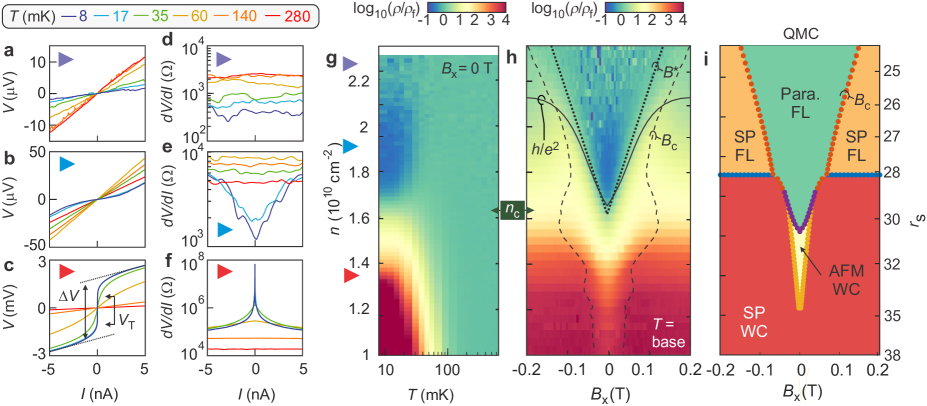
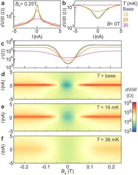
Non-linear charge transport is encountered throughout the parameter space and is revealed by studying the differential resistance as a function of current. Figures 4a-c plot traces at three distinct charge densities, corresponding to , 28 and 32, respectively (purple, blue and red triangle). The corresponding differential resistance as a function of is plotted in panels d-f. The three values of represent qualitatively distinct responses in the ()-parameter space. For the system displays metallic () transport as the lowest attainable temperature is approached, with approximately constant as a function of . In contrast, strong non-linearity develops in the voltage response as when . We characterize this nonlinearity in two different ways: through the threshold voltage () at which 10 pA flows through the device, and through an extrapolation of the high current voltage drop to zero current (), as shown in panel c. A large is a characteristic transport feature expected from a WC ground state,Knighton et al. (2018) arising from pinning of the crystal. We also identify a regime of apparent excess conductance at low bias for a finite range of densities, 1010 cm-2 (panels b,e). In this regime, a flattening of the voltage drop as a function of current is visually apparent in the raw data (Fig. 4b), producing a lower differential resistance as . The differential resistance increases by as much as times when even a few nanoamperes of current (corresponding to fW power dissipation) are fed through the device. This excess conductance is discussed further below.
Figures 4g and h plot the ratio of zero-bias and finite-bias resistances, , in the ()-plane at zero field (Fig. 4g), and in the ()-plane at base temperature (Fig. 4h). Here, corresponds to the differential resistance at a finite current of approximately 5 nA. The green regions (for which is close to zero) in these maps correspond to a linear response, for which the differential resistance is independent of , as is evident for all when mK. Some region of excess conductivity, defined as , appears as a small dome-like blue region above , disappears above 30 mK, and is suppressed with the application of a -field (see Fig.S15). Similar features have been identified in previous studies as the MIT is approached.Kravchenko et al. (1996); Yoon et al. (1999) Both yellow and red regions corresponds to a peak in at nA, with the the former displaying weaker non-linearity in the form of a finite and the latter hosting a prominent as .
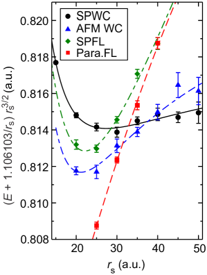
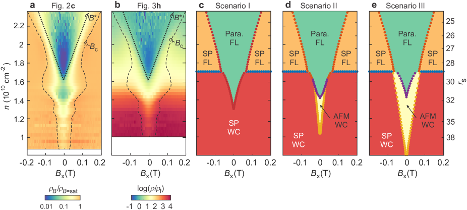
We will now discuss the underlying nature of the phases encountered. We characterize the phases using the boundaries associated with full spin polarization of the system (, dashed line), the change in sign of (, dotted line), the magnitude of the resistivity relative to (black line), and the degree of non-linearity (), all of which are plotted in Fig.4h. We couple these experimental results with a comparison to state-of-the-art QMC simulationsDrummond and Needs (2009), which have identified a competition between paramagnetic FL (Para. FL), spin polarized FL (SP FL), antiferromagnetic WC (AFM WC) with a stripe-like spin order on a triangular lattice and spin-polarized WC (SP WC) phases in the range studied in our work. Here we expand the phase diagram produced by QMC to take into account a finite in-plane magnetic field (see SI for details and alternative scenarios). The result is presented in Fig.4i and contains no free parameters.
We can confidently associate the zero field metal phase at large with a paramagnetic FL subjected to increasingly strong interactions as is reduced towards . At finite and , however, the change in sign of at that is traditionally associated with a MIT bears closer resemblance to a linear-in- correction to the conductivity emerging from strong interactions in a FL.Zala et al. (2001a, b) We also note that magnetic field scale at which the paramagnetic FL is predicted by QMC calculations to become the SP FL (Fig.4i) agrees very well with the measured value of (or ) without any fitting parameters. Therefore we associate the state that appears for and as the spin polarized FL. However, while such a linear increase is consistent with our data (see SI Sec. S7), we caution that the theory is not a priori applicable to the states with relatively large and large resistivity that we are considering. In line with this concern, it is worth emphasizing that our results in this regime exhibit extreme deviations from the usual weak-coupling metallic conductivity, as evidenced, for example, by the enormous positive magnetoresistance and by a low temperature resistivity substantially higher than .
Turning our attention to , the insulating phase has the characteristic transport attributes of a pinned WC, as evidenced by the large value of that develops at low temperature. The non-linearity in this regime is orders of magnitude larger than that of the SP FL phase discussed above, supporting our hypothesis that the two regimes host distinct phases. The positive magnetoresistance at that becomes increasing clear at very low temperatures in Fig. 3c remains to be fully understood, although it is apparently consistent with calculationsMatveev et al. (1995) that consider the effect of Zeeman splitting of localized states on hopping conduction. The presence of finite magnetoresistance appears to preclude the conclusion that the state is fully spin polarized at low temperature in the range of studied. This is in contrast with a recent study of AlAs Hossain et al. (2020), which reported an apparent divergence of the spin susceptibility in the insulating phase based upon a flat magnetoresistance for at a measurement temperature of K. The lack of clear spontaneous spin-polarization at very low temperatures in our experiment is in agreement with the fact that the exchange energy scale associated with spin ferromagnetic ordering of the WC at , as estimated by QMC, is smaller than mK. The spins of the WC are therefore likely disordered by temperature fluctuations at . While we note that delicate hysteretic features in transport are indeed resolved for which upon first glance could indicate some FM ordering (see Fig.S7), we, however, ascribe these features to experimental artifacts associated with heating close to zero field and trapped flux in the superconducting coil, as the estimated coercive field in the presence of magnetostatic fields is T (see section S5) and hence undetectable in experiment.
Finally, we would like to discuss one of the most remarkable findings of our study, namely the non-monotonicity of the in-plane saturation field near the zero field MIT. The non-monotonicity of is a low temperature property of the system and is absent above approximately 30 mK (see Fig.S4). In agreement with state-of-the-art QMC calculations,Drummond and Needs (2009) we find no clear evidence for a Stoner instability of the itinerant liquid; finite magnetoresistance is always present in the metal phase. In contrast, QMC has identified a possible AFM crystal in between the paramagnetic FL and the fully SP WC. By adapting the QMC results from Ref. Drummond and Needs, 2009 to include in-plane field (see SI section S3.1 for details), one obtains the phase diagram shown in Fig.4i. However, as we see from this phase diagram, the intermediate AFM does not offer any clear explanation for the non-monotonicity of the critical field to spin polarize the system. Moreover, as mentioned before, our lowest temperature scale mK is larger than the exchange energy scale , or more precisely it is larger than the energy difference per electron of the FM WC and the AFM WC obtained from QMC, as detailed in SI Sec. S6, and thus the spin order of the WC is likely destroyed by temperature fluctuations at . We therefore believe that the AFM WC phase found in QMC is not likely to be the origin of the non-monotonicity of that we observe. We note that the QMC employed in Ref.Drummond and Needs, 2009 is variational in nature and therefore it is always possible that other phases not considered could be behind the non-monotonicity of , such as exotic spin liquid statesChakravarty et al. (1999); Bernu et al. (2001) or spin-density-wave ordered states like those suggested by Hartree-Fock studies Bernu et al. (2011, 2017).
The role of spatial variation in electron density may also be prominent in the vicinity of . Even in the cleanest samples it is not possible to completely eliminate the role of disorder, which tends to produce variation in the local electron density. When the average density is very close to , such variation causes the 2DES to break up into itinerant and localized regions. (See SI Sec. S8 for a more detailed discussion of disorder-induced density modulation.) And even in the absence of disorder, variation in the local density can arise from Coulomb-frustrated phase separation.Spivak and Kivelson (2004); Jamei et al. (2005); Spivak and Kivelson (2006); Li et al. (2019) While such phase separation may be important near , it does not provide an obvious explanation for the nonmonotonicity of as a function of . Still, the phase separation picture can serve as a premise for interpreting the apparent excess conductance presented in Figs. 4b and e. When conducting and insulating phases are mixed in nearly equal proportion, then electric current flows predominantly through narrow metallic pathways, which are unusually sensitive to joule heating. The ratio of metallic to insulating regions falls as the MIT is approached, with the MIT signifying the transition to a regime where insulating regions percolate and metallic regions are relegated to disconnected puddles. An extended discussion of this scenario is presented in SI section S9.
In summary, our study provides an unprecedented level of experimental clarity about the phase diagram around the Wigner crystallization transition at and very low temperatures. Our data reveals a paramagnetic FL which exhibits a strong renormalization of its spin susceptibility as the critical density is approached, with the spin susceptibility becoming nearly 30 times larger than the band value. At the transport becomes strongly nonlinear and exhibits an exponential temperature dependence, both of which features are consistent with a WC. The qualitative and quantitative agreement of our phase diagram with state-of-the-art QMCDrummond and Needs (2009) is striking with zero adjustable parameters. The most prominent mystery suggested by our measurements is the possible existence and nature of a WC state with incomplete spin polarization. The non-monotonicity of the magnetic field required to achieve spin polarization has no obvious interpretation in terms of the QMC phase diagram, and may be associated with either spatial coexistence of different phases or with an as-yet undetermined intermediate phase. The large increase of resistance with in-plane field, which for densities near becomes as large as two orders of magnitude, is also incompletely understood. QMC calculations suggest that the state at and slightly larger than is a spin polarized FL, but the large value of resistance poses a challenge for understanding this state within traditional paradigms of metallic transport.
Methods
The heterostructure was grown using ozone-assisted molecular beam epitaxy and consists of a lightly alloyed MgxZn1-xO layer ( 0.001) of 500 nm thickness grown on a homoepitaxial ZnO layer upon single crystal (0001) Zn-polar ZnO substrates.J. Falson and Y. Kozuka and M. Uchida and J. H Smet and T. Arima and A. Tsukazaki and M. Kawasaki (2016); Falson and Kawasaki (2018) The heterostructure has an electron mobility approaching 106 cm2/Vs in the metallic regime. Ohmic contacts were formed by evaporating Ti (10nm) followed by Au (50nm) on the sample surface. Indium was additionally soldered upon these pads to improve the contact quality. The distance between voltage probes is approximately 1 mm. The sample was immersed in a liquid 3He containing polycarbonate cell attached to the end of a cold finger of a dilution refrigerator cryostat (650W cooling power at 120 mK) equipped with a 3-axis (9-3-1 T) vector magnet. The 3He cell is based upon the design used in other ultra-low temperature experiments on high mobility 2DES.Pan et al. (1999) The mixing chamber temperature is measured using a calibrated cerous magnesium nitrate paramagnetic thermometer for mK, and a ruthenium oxide thermometer for mK. Each measurement wire is passed through a large surface area (1 m2) sintered silver heat exchanger to overcome the Kapitza interfacial resistance that suppresses heat exchange at low . The differential resistance data is obtained by measuring - data using DL Instruments 1211 current and 1201 voltage preamplifiers at discrete steps in the () parameter space, followed by differentiation using data analysis software.
Acknowledgments
We appreciate discussions with Joe Checkelsky, Neil Drummond, Jim Eisenstein, Andrea Young, Steve Kivelson, Boris Spivak, and Chaitanya Murthy, along with technical support from Jian-Sheng Xia, Neil Sullivan and Gunther Euchner. M.K. acknowledge the financial support of JST CREST Grant Number JPMJCR16F1, Japan. Y.K. acknowledges JST, PRESTO Grant Number JPMJPR1763, Japan. J.F. acknowledges support from the Max Planck Institute–University of British Columbia–University of Tokyo Center for Quantum Materials, the Deutsche Forschungsgemeinschaft (DFG) (FA 1392/2-1) and the Institute for Quantum Information and Matter, an NSF Physics Frontiers Center (NSF Grant PHY-1733907).
References
- Tanatar and Ceperley (1989) B. Tanatar and D. M. Ceperley, Phys. Rev. B 39, 5005 (1989), URL https://link.aps.org/doi/10.1103/PhysRevB.39.5005.
- Rapisarda and Senatore (1996) F. Rapisarda and G. Senatore, Australian journal of physics 49, 161 (1996).
- Phillips et al. (1998) P. Phillips, Y. Wan, I. Martin, S. Knysh, and D. Dalidovich, Nature 395, 253 (1998).
- Chamon et al. (2001) C. Chamon, E. R. Mucciolo, and A. H. Castro Neto, Phys. Rev. B 64, 245115 (2001), URL https://link.aps.org/doi/10.1103/PhysRevB.64.245115.
- Attaccalite et al. (2002) C. Attaccalite, S. Moroni, P. Gori-Giorgi, and G. B. Bachelet, Phys. Rev. Lett. 88, 256601 (2002), URL https://link.aps.org/doi/10.1103/PhysRevLett.88.256601.
- Spivak and Kivelson (2004) B. Spivak and S. A. Kivelson, Phys. Rev. B 70, 155114 (2004), URL https://link.aps.org/doi/10.1103/PhysRevB.70.155114.
- Drummond and Needs (2009) N. D. Drummond and R. J. Needs, Phys. Rev. Lett. 102, 126402 (2009), URL https://link.aps.org/doi/10.1103/PhysRevLett.102.126402.
- Spivak et al. (2010) B. Spivak, S. V. Kravchenko, S. A. Kivelson, and X. P. A. Gao, Rev. Mod. Phys. 82, 1743 (2010), URL https://link.aps.org/doi/10.1103/RevModPhys.82.1743.
- Abrahams et al. (2001) E. Abrahams, S. V. Kravchenko, and M. P. Sarachik, Rev. Mod. Phys. 73, 251 (2001), URL https://link.aps.org/doi/10.1103/RevModPhys.73.251.
- Kravchenko and Sarachik (2003) S. V. Kravchenko and M. P. Sarachik, Reports on Progress in Physics 67, 1 (2003), URL https://doi.org/10.1088/0034-4885/67/1/r01.
- Shashkin and Kravchenko (2019) A. A. Shashkin and S. V. Kravchenko, Applied Sciences 9 (2019), ISSN 2076-3417, URL https://www.mdpi.com/2076-3417/9/6/1169.
- Dolgopolov (2019) V. T. Dolgopolov, Physics-Uspekhi 62, 633 (2019), URL https://doi.org/10.3367/ufne.2018.10.038449.
- Yoon et al. (1999) J. Yoon, C. C. Li, D. Shahar, D. C. Tsui, and M. Shayegan, Phys. Rev. Lett. 82, 1744 (1999), URL https://link.aps.org/doi/10.1103/PhysRevLett.82.1744.
- Knighton et al. (2018) T. Knighton, Z. Wu, J. Huang, A. Serafin, J. S. Xia, L. N. Pfeiffer, and K. W. West, Phys. Rev. B 97, 085135 (2018), URL https://link.aps.org/doi/10.1103/PhysRevB.97.085135.
- Hossain et al. (2020) M. S. Hossain, M. K. Ma, K. A. V. Rosales, Y. J. Chung, L. N. Pfeiffer, K. W. West, K. W. Baldwin, and M. Shayegan, Proceedings of the National Academy of Sciences 117, 32244 (2020), ISSN 0027-8424, eprint https://www.pnas.org/content/117/51/32244.full.pdf, URL https://www.pnas.org/content/117/51/32244.
- Falson et al. (2015) J. Falson, D. Maryenko, B. Friess, D. Zhang, Y. Kozuka, A. Tsukazaki, J. H. Smet, and M. Kawasaki, Nature Physics 11, 347 (2015).
- Falson et al. (2018) J. Falson, D. Tabrea, D. Zhang, I. Sodemann, Y. Kozuka, A. Tsukazaki, M. Kawasaki, K. von Klitzing, and J. H. Smet, Science Advances 4, eaat8742 (2018).
- Kozuka et al. (2013) Y. Kozuka, S. Teraoka, J. Falson, A. Oiwa, A. Tsukazaki, S. Tarucha, and M. Kawasaki, Phys. Rev. B 87, 205411 (2013), URL https://link.aps.org/doi/10.1103/PhysRevB.87.205411.
- Shklovskii and Efros (1984) B. I. Shklovskii and A. L. Efros, Electronic Properties of Doped Semiconductors (Springer-Verlag, New York, 1984).
- Shklovskii (2004) B. I. Shklovskii, physica status solidi (c) 1, 46 (2004), eprint https://onlinelibrary.wiley.com/doi/pdf/10.1002/pssc.200303642, URL https://onlinelibrary.wiley.com/doi/abs/10.1002/pssc.200303642.
- Zala et al. (2001a) G. Zala, B. N. Narozhny, and I. L. Aleiner, Phys. Rev. B 65, 020201 (2001a), URL https://link.aps.org/doi/10.1103/PhysRevB.65.020201.
- Zala et al. (2001b) G. Zala, B. N. Narozhny, and I. L. Aleiner, Phys. Rev. B 64, 214204 (2001b), URL https://link.aps.org/doi/10.1103/PhysRevB.64.214204.
- Kravchenko et al. (1996) S. V. Kravchenko, D. Simonian, M. P. Sarachik, W. Mason, and J. E. Furneaux, Phys. Rev. Lett. 77, 4938 (1996), URL https://link.aps.org/doi/10.1103/PhysRevLett.77.4938.
- Matveev et al. (1995) K. A. Matveev, L. I. Glazman, P. Clarke, D. Ephron, and M. R. Beasley, Phys. Rev. B 52, 5289 (1995), URL https://link.aps.org/doi/10.1103/PhysRevB.52.5289.
- Chakravarty et al. (1999) S. Chakravarty, S. Kivelson, C. Nayak, and K. Voelker, Philosophical Magazine B 79, 859 (1999), eprint https://doi.org/10.1080/13642819908214845, URL https://doi.org/10.1080/13642819908214845.
- Bernu et al. (2001) B. Bernu, L. Cândido, and D. M. Ceperley, Phys. Rev. Lett. 86, 870 (2001), URL https://link.aps.org/doi/10.1103/PhysRevLett.86.870.
- Bernu et al. (2011) B. Bernu, F. Delyon, M. Holzmann, and L. Baguet, Phys. Rev. B 84, 115115 (2011), URL https://link.aps.org/doi/10.1103/PhysRevB.84.115115.
- Bernu et al. (2017) B. Bernu, F. Delyon, L. Baguet, and M. Holzmann, Contributions to Plasma Physics 57, 524 (2017), eprint https://onlinelibrary.wiley.com/doi/pdf/10.1002/ctpp.201700139, URL https://onlinelibrary.wiley.com/doi/abs/10.1002/ctpp.201700139.
- Jamei et al. (2005) R. Jamei, S. Kivelson, and B. Spivak, Phys. Rev. Lett. 94, 056805 (2005), URL https://link.aps.org/doi/10.1103/PhysRevLett.94.056805.
- Spivak and Kivelson (2006) B. Spivak and S. A. Kivelson, Annals of Physics 321, 2071 (2006), ISSN 0003-4916, URL http://www.sciencedirect.com/science/article/pii/S0003491605002654.
- Li et al. (2019) S. Li, Q. Zhang, P. Ghaemi, and M. P. Sarachik, Phys. Rev. B 99, 155302 (2019), URL https://link.aps.org/doi/10.1103/PhysRevB.99.155302.
- J. Falson and Y. Kozuka and M. Uchida and J. H Smet and T. Arima and A. Tsukazaki and M. Kawasaki (2016) J. Falson and Y. Kozuka and M. Uchida and J. H Smet and T. Arima and A. Tsukazaki and M. Kawasaki, Scientific reports 6, 26598 (2016).
- Falson and Kawasaki (2018) J. Falson and M. Kawasaki, Reports on Progress in Physics 81, 056501 (2018).
- Pan et al. (1999) W. Pan, J.-S. Xia, V. Shvarts, D. E. Adams, H. L. Stormer, D. C. Tsui, L. N. Pfeiffer, K. W. Baldwin, and K. W. West, Phys. Rev. Lett. 83, 3530 (1999), URL https://link.aps.org/doi/10.1103/PhysRevLett.83.3530.
- Solovyev et al. (2015) V. V. Solovyev, A. B. Van’kov, I. V. Kukushkin, J. Falson, D. Zhang, D. Maryenko, Y. Kozuka, A. Tsukazaki, J. H. Smet, and M. Kawasaki, Applied Physics Letters 106, 082102 (2015), eprint https://doi.org/10.1063/1.4913313, URL https://doi.org/10.1063/1.4913313.
- Zorin (1995) A. B. Zorin, Review of Scientific Instruments 66, 4296 (1995), eprint https://doi.org/10.1063/1.1145385, URL https://doi.org/10.1063/1.1145385.
- Pines (2018) D. Pines, Theory of Quantum Liquids: Normal Fermi Liquids (CRC Press, 2018).
- Tsukazaki et al. (2008) A. Tsukazaki, A. Ohtomo, M. Kawasaki, S. Akasaka, H. Yuji, K. Tamura, K. Nakahara, T. Tanabe, A. Kamisawa, T. Gokmen, et al., Phys. Rev. B 78, 233308 (2008), URL https://link.aps.org/doi/10.1103/PhysRevB.78.233308.
- Kozuka et al. (2012) Y. Kozuka, A. Tsukazaki, D. Maryenko, J. Falson, C. Bell, M. Kim, Y. Hikita, H. Y. Hwang, and M. Kawasaki, Phys. Rev. B 85, 075302 (2012), URL https://link.aps.org/doi/10.1103/PhysRevB.85.075302.
- Shashkin et al. (2002) A. A. Shashkin, S. V. Kravchenko, V. T. Dolgopolov, and T. M. Klapwijk, Phys. Rev. B 66, 073303 (2002), URL https://link.aps.org/doi/10.1103/PhysRevB.66.073303.
- Lilly et al. (2003) M. P. Lilly, J. L. Reno, J. A. Simmons, I. B. Spielman, J. P. Eisenstein, L. N. Pfeiffer, K. W. West, E. H. Hwang, and S. Das Sarma, Phys. Rev. Lett. 90, 056806 (2003), URL https://link.aps.org/doi/10.1103/PhysRevLett.90.056806.
- Zabrodskii and Zinov’eva (1984) A. Zabrodskii and K. Zinov’eva, JETP 59, 425 (1984), URL http://www.jetp.ac.ru/cgi-bin/e/index/e/59/2/p425?a=list.
- Shashkin et al. (2001) A. A. Shashkin, S. V. Kravchenko, and T. M. Klapwijk, Phys. Rev. Lett. 87, 266402 (2001), URL https://link.aps.org/doi/10.1103/PhysRevLett.87.266402.
- Ando et al. (1982) T. Ando, A. B. Fowler, and F. Stern, Reviews of Modern Physics 54, 437 (1982), publisher: American Physical Society, URL https://link.aps.org/doi/10.1103/RevModPhys.54.437.
- Skinner and Shklovskii (2013) B. Skinner and B. I. Shklovskii, Physical Review B 87, 075454 (2013), publisher: American Physical Society, URL https://link.aps.org/doi/10.1103/PhysRevB.87.075454.
- Bello et al. (1981) M. S. Bello, E. I. Levin, B. I. Shklovskii, and A. L. Efros, Sov. Phys. JETP 53, 822 (1981).
- Eisenstein et al. (1992) J. P. Eisenstein, G. S. Boebinger, L. N. Pfeiffer, K. W. West, and S. He, Phys. Rev. Lett. 68, 1383 (1992), URL https://link.aps.org/doi/10.1103/PhysRevLett.68.1383.
- Li et al. (2013) Q. Li, J. Zhang, J. Chong, and X. Hou, Applied Physics Express 6, 121102 (2013), URL https://doi.org/10.7567/apex.6.121102.
- Maryenko et al. (2018) D. Maryenko, A. McCollam, J. Falson, Y. Kozuka, J. Bruin, U. Zeitler, and M. Kawasaki, Nature communications 9, 4356 (2018).
- Vitkalov et al. (2001) S. A. Vitkalov, H. Zheng, K. M. Mertes, M. P. Sarachik, and T. M. Klapwijk, Phys. Rev. Lett. 87, 086401 (2001), URL https://link.aps.org/doi/10.1103/PhysRevLett.87.086401.
- Kapitulnik et al. (2019) A. Kapitulnik, S. A. Kivelson, and B. Spivak, Rev. Mod. Phys. 91, 011002 (2019), URL https://link.aps.org/doi/10.1103/RevModPhys.91.011002.
Supplementary Information
S1 Sample parameters
| Parameter | Magnitude | Units |
|---|---|---|
| 3.5 | m-1 | |
| 1.6 | eV | |
| 1.85 | K | |
| 100 | s | |
| 1.5 | m | |
| 27 | ||
| 1.3 | m-1 | |
| 10 | m |
Table 1 collects relevant parameters of the MgZnO/ZnO 2DES when 1010 cm-2 and cm2/Vs. Here, is the Fermi momentum, the kinetic energy, the Fermi temperature, the transport scattering time, the mean free path of conduction, the ratio between Coulomb and kinetic energy, the Thomas-Fermi screening wave length, and an estimate of the wavefunction thickness, based on the data presented in Ref. Solovyev et al., 2015. Note that the band effective mass is used in these calculations. The use of the renormalized mass values will be discussed in the subsequent sections. The peak electron mobility of the device is approximately 600,000 cm2/Vs. Ohmic contacts were formed by evaporating Ti (10 nm) followed by Au (50 nm) on the sample surface. Indium was additionally soldered upon these pads to improve the contact quality. Qualitatively similar results were obtained both with and without this additional indium layer.

S2 Measurement details
All measurements have taken place in a 3He immersion cell anchored at the base of an annealed silver cold finger attached to the mixing chamber of a 650W at 120 mK dilution refrigerator (base mK). The cell design is based on the one utilized at the National High Magnetic Field Laboratory High B/T facility in Gainesville, Florida. This technique has proven powerful in achieving the low electron temperatures required for studies of delicate fractional quantum Hall features,Pan et al. (1999) and also insulating phases in low density 2DES devices.Knighton et al. (2018) The mixing chamber temperature is measured using a calibrated cerous magnesium nitrate paramagnetic thermometer for mK, and a ruthenium oxide thermometer for mK. These thermometers have good overlap in the range 50120 mK. We do not measure the temperature inside the 3He cell. As electrons at low temperature are actively cooled primarily via electrical contacts at ultra-low temperatures, the exact electron temperature is dependent on the contact resistance. The Kapitza phonon interfacial resistance () may be effectively suppressed by immersing the sample in the cryogen and attaching large surface area () sintered silver heat exchangers to each measurement wire. Electrical signals are carried from room temperature down to the mixing chamber using individual thermocoax lines, each with a length of approximately 2 m. These lines are thermally anchored at the 1 K, still, 50 mK and mixing chamber plates. These cables act as distributed R-C filters and are effective in attenuating stray radiation in cryogenics applications.Zorin (1995) They consist of a resistive stainless steel inner conductor ( ) isolated from the outer conductor by a MgO nanoparticle dielectric. The skin effect of the nanoparticles strongly attenuates high frequency signals ( MHz). An additional R-C filter is employed at the mixing chamber. Superconducting Nb-Ti loom is used between the mixing chamber and the measurement puck.
Magnetic flux is generated by a 3-axis (9-3-1 T) superconducting vector magnet. The cryostat is suspended above a pit carved into a 35 ton concrete block that is subsequently isolated from the main building structure by vibration dampening pads. Circulation pumps are anchored to the outer wall of the superstructure to reduce vibrations. The measurement room is electrically isolated from the outside environment by a Faraday cage delivering -60 dBm attenuation. Measurement electronics are powered by a dedicated phase of a three-phase power supply, operate on individual isolating transformers, and are isolated from the data gathering measurement computer by an optical isolator. Significant efforts, such as electrically isolating the cryostat from pumps and diagnostics electronics, have been taken to minimize ground-loops within the measurement circuitry. We strive to utilize low-noise electronics for measurements, such as all analogue lock-in amplifiers (PAR 124A) (only used for the data presented in Fig.S12), Yokogawa 7651 DC voltage sources and DL Instruments voltage (1201) and current (1211) preamplifiers.
DC measurement techniques often incorporate offsets in both the current and voltage signal. These offsets can also fluctuate in time. We have tried to reduce this uncertainty by ensuring excellent temperature stability of the laboratory, while maintaining electrical power to the electronics at all times. The current offset is addressed by adjusting the zero offset of the current preamplifier at zero applied electric field. The voltage offsets are more challenging to eliminate with features order of nano- to microvolts between individual IV sweeps being observed. The only point where we have adjusted the data in this manuscript is in Fig.4a-c and S16, where we take the measured voltage at zero current at a set temperature and charge density and subtract it as an offset for each trace. The process of differentiating data eliminates this offset as it is only sensitive to the slope of the data.
S3 Monte-Carlo Phase Diagrams of 2D Jellium
The analysis we present here relies on the variational Monte-Carlo study of Ref. Drummond and Needs, 2009. This study compared energies of four states: a spin unpolarized paramagnetic Fermi liquid (Para. FL), spin polarized Fermi liquid (SP FL), spin unpolarized Wigner crystal (AFM WC) with a stripe-like spin antiferromagnetic order and a triangular lattice and a spin polarized Wigner crystal (SP WC) with triangular lattice. The main results of Ref. Drummond and Needs, 2009 are adapted in Fig. S2, and imply that as increases, the ground state progresses from Para. FL, to AFM WC, to SP WC, in the vicinity of . Importantly, Ref. Drummond and Needs, 2009 ruled out the possibility of the traditional Stoner transition from Para. FL to a SP FL.
We use this study to estimate the phase diagram as a function and . Because electrons in ZnO have weak spin-orbit coupling, the total spin of the system is a good quantum number. This allows us to know the exact energy of each of the four states previously described, which are all either fully spin polarized or fully spin un-polarized. However, to have a complete phase diagram we need to estimate the energy of potential states with different partial polarization. To do this, it is unavoidable to make certain assumptions about the dependence of the energy on spin polarization. We therefore analyze the competition of these phases within three distinct scenarios. As we will see the main conclusions are relatively robust to the assumptions within different scenarios.
S3.1 Scenario I: phase diagrams without a partially polarized crystal
The appearance of a possible competing intermediate crystal is a relatively new development within the series of Monte-Carlo studies of the ideal Jellium model Drummond and Needs (2009), although indications of such an intermediate state appeared in a previous study Bernu et al. (2001), and also in self-consistent Hartree-Fock calculations Bernu et al. (2011, 2017). Since most previous studies did not find or ignored the possibility of these partially polarized crystalline states, it is natural to try to determine what would be the phase diagram if such states are not considered as part of the competing states. To do so we begin by approximating the ground state energy per electron of the Fermi liquids as a function of their spin polarization polarization , given by
| (S3) |
with a simple parabolic dependence, as follows:
| (S4) |
Here and are the energies of the unpolarized FL and spin polarized FL phases from Ref. Drummond and Needs, 2009 and the -factor is .Kozuka et al. (2013) Notice from Fig. S2 that since for our range of interest , there is always an energy penalty for polarizing the Fermi liquid, and no Stoner transition. In this first scenario, these states compete only with a PWC, whose energy is
| (S5) |
where is the energy of spin polarized WC from Ref. Drummond and Needs, 2009. For each we find the FL state with the optimal polarization and determine its energy competition with the WC. The resulting phase diagram is shown in Fig. S3c.
S3.2 Scenario II: phase diagrams with a partially polarized crystal with a first order transition
We now include the possibility of a partially polarized (AFM) WC and model its energy using the same parabolic dependence we used for the FL, as follows:
| (S6) |
The phase diagrams obtained by comparing these energies from those of the FL states from Eq. (S4) is shown in Fig. S3d. Notice that since there is a crossing of the energies of SPWC and AFM WC around (see Fig. S2), the above form predicts a first-order spin-flop-type transition of the spin polarization among the WC states at . There is a priori no reason favoring this transition to be first order rather than continuous, which leads us to consider this scenario separately.
S3.3 Scenario III: phase diagrams with a partially polarized crystal with a continuous transition
In order to account for a possible continuous transition of the spin polarization of the partially polarized Wigner crystal into the fully polarized crystal, we parameterize their energy dependence on spin polarization with a simple quartic Ginzburg-Landau (GL) form:
| (S7) |
As customary for GL quartic functionals, we take the coefficient to be positive for all . The crystal starts developing a non-zero spontaneous spin-polarization at a certain density , for which the coefficient changes from positive to negative. For the GL functional predicts a monotonically increasing spontaneous polarization, until the system saturates at at some second density . With these inputs the coefficients of the GL functional can be fixed to be:
| (S8) |
| (S9) |
Since the Monte Carlo study Drummond and Needs (2009) did not explore partially polarized states, the precise values of and are unknown, although they should satisfy . The phase diagram shown in Fig. S3e has been made by choosing and . The precise of form of the phase diagram does not have strong sensitivity on the precise values of and , provided they are chosen in the vicinity of up to some distance of about . In fact, in the limiting case in which the polarization changes rapidly from unpolarized to polarized, approaches and one recovers the Scenario II of a first order transition. The main difference is a reduction in size of the region where the partially polarized crystal is energetically favored, but the overall shape of the two phase diagrams still looks reasonably similar in both scenarios II and III, shown in Fig. S3d and e.
S4 Landau Fermi liquid parameters
The energy density of the metallic system at fixed density in the presence of an in-plane Zeeman field, , is given by
| (S10) |
where is the spin density, the spin susceptibility, is the -factor, and is the Bohr magneton. Therefore, the critical field, , at which the system fully spin polarizes at a given total density, , provides an approximate measure of the spin susceptibility of the system:
| (S11) |
In Landau Fermi liquid theory, this susceptibility is expressed in terms of the quasiparticle mass (), the bare band mass (), the bare spin susceptibility () and the Landau parameter as follows Pines (2018):
| (S12) |
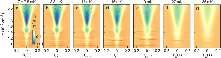
The spin susceptibility of carriers can be evaluated by various means. A strategy we have employed in previous studies is the coincidence method which relies on rotating the sample within a magnetic field to study transport features associated with the crossing of opposing spin Landau levels.Tsukazaki et al. (2008); Falson et al. (2015, 2018) In addition to the coincidence method, it is possible to polarize carriers into a single spin band by applying an in-plane magnetic field. According to Eq.S11, identification of a critical field leads to the quantification of . This measurement is discussed in the main text in the context of Fig. 3 with saturation of the magnetoresistance at a critical field being taken as evidence for full spin polarization. For the sake of completeness, here we present the full raw data set used to produce the analysis presented in Fig. 2 of the main text. This data set comprises multiple maps of the differential resistance in the (,)-parameter space at a number of set temperatures. These are all presented in Fig. S4. As in Fig. 2c, we plot the ratio , where is the saturated differential resistance at a set charge density at high magnetic field (corresponding to full spin polarization). The characteristic positive magnetoresistance is evident for all at high , but is difficult to discern in the higher mK data upon depletion of the 2DES.
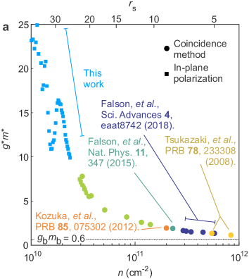
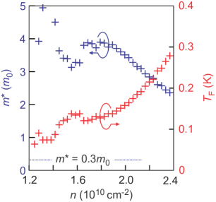
The renormalization of band parameters in the ZnO-based 2DES as a function of charge density is summarized in Fig. S5. This figure is compiled from values reported in previous publicationsKozuka et al. (2012); Falson et al. (2015, 2018), the devices presented in this manuscript, along with other unpublished results gathered on samples characterized in the course of this project. Values obtained through the coincidence method are displayed as circles, with squares representing those gained through analyzing the positive magnetoresistance of a polarizing in-plane magnetic field. The error associated with each point is no larger than the symbol size. A good agreement between these two methods is obtained for the range of densities shown. We additionally display the corresponding value at each on the top axis. Previous studies on Si-based devices identified that the enhancement of the spin susceptibility as the critical density is approached is associated with an enhancement of the effective mass.Shashkin et al. (2002)
Utilizing the experimentally obtained and working under the assumption that the parameter enhancement is primarily due to the renormalization of the effective mass,Falson and Kawasaki (2018) we can extract the mass value and renormalized Fermi temperature () as a function of . This is plotted in Fig. S6. According to Ref. [Lilly et al., 2003], a local “peak” in of dilute GaAs-based 2DES emerges as becomes comparable but smaller than given , where =2 2.4 K is the Bloch-Grüneissen temperature calculated using m/s as the average between transverse and longitudinal sound velocities in ZnO and 1010 cm-2. Being deep in the Bloch-Grüneissen regime, phonon scattering contributes little to the resistivity. A local peak in is an experimental feature is observed in our data for 1010 cm-2. The calculated values are those presented in Fig.S10. The local maximum in when occurs just below the calculated . We note that the corresponding calculated Fermi temperature is in the range K utilizing the band mass.
S5 Absence of magnetostatically induced hysteresis and domains in ferromagnetic phases
Here we estimate the typical value of the coercive fields associated with magnetic hysteresis arising from magneto-static fields. Our goal is to argue that these fields are too small to be responsible for any observed behavior in our samples. We clarify that our argument does not imply that the system cannot, in principle, display hysteresis via other mechanisms, such as metastability associated with pinning of the Wigner crystal. But we are able to argue that the non-trivial in-plane field dependence of the resistivity of the insulating state, seen in Fig.3b of main text, cannot be a result of magnetic-field-induced ferromagnetic domain alignment of the putative ferromagnetic Wigner crystal.
Since ZnO has negligible spin-orbit coupling, the formation of magnetic domains and hysteresis is dictated by magneto-statics. Assuming that each electron contributes one Bohr magneton, , to the magnetization in the spin polarized state, the coercive field scale (the magnetic field width of hysteresis loop) can be estimated to be:
| (S13) |
where is the vacuum magnetic permeability constant, is the average volume per electron, and nm is the effective well width of the 2DES in ZnO. For we have:
| (S14) |
The smallness of this scale is ultimately a consequence of the tremendous diluteness of our systems. Each electron occupies a 3D volume of about Å3, which is about larger than in ordinary 3D metals such as copper. The above strongly indicates that magnetostatic domain formation is completely negligible.
We now present our experimental data close to zero field for the sake of completeness. After much effort to properly understand these effects, we emphasize that it is extremely difficult to eliminate all parasitic effects when collecting the data. There are a number of experimental unknowns that are difficult to avoid. Firstly we mention temperature fluctuations when sweeping the magnetic field due to the presence of nuclear and electron spin magnetization processes. These may occur in the sample, electrical contacts, experimental wiring, and materials used to construct the helium immersion cell. Furthermore, it is very difficult to exclude the influence of remnant magnetic flux in the superconducting magnet system used.
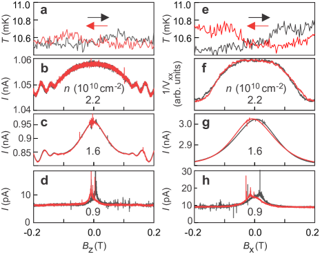
Figure S7 presents sweep-direction-dependent electrical characteristics of the device measured. The sample is biased with a DC voltage that produces approximately 1 nA when charge is accumulated and the sample is metallic. Panels a-d present data when the field is projected in the direction, with e-g presenting data in the direction. We measure the thermometer reading at the mixing chamber through these sweeps, which are performed at a very low rate of 1 mT/min, as shown in panels a and e. Sweeping conveniently reveals quantum oscillations, whose period are known to be determined by the magnetic flux penetrating the sample, and therefore may be used to reduce the uncertainty of remnant flux in the coil at low field by forcing the oscillation minima in up-sweep and down-sweep data to overlap. Panels b-d and f-h present sweeps at three distinct charge densities, corresponding to the metallic, critical and insulating portions of the parameter space. Within our detection limit, the up- and down-sweep data overlap closely, as shown in panel b. Operating under the assumption that hysteresis is weak or absent at this charge density, we enforce up- and down-sweep data to overlap measured in the direction, as shown in panel f. This process establishes a remnant flux of approximately 5 mT in the and 15 mT in the coils. This value is used to manually offset subsequent field sweeps performed in a repetitive cycle in an attempt to reduce the impact of this parasitic effect. Next, we can vary the charge density of the device, as plotted in panels c and g when is close to . While higher field quantum oscillations overlap nicely in the data set, additional delicate features close to in the form of sharp spikes in the data are resolved in both projections of the magnetic field. These become even more evident upon reducing below . While these features occur at fields where the temperature read during up and down sweeps coincides, it is not possible for us to know what is occurring locally at the sample. These features do not follow a Curie-Weiss-like temperature dependence and are robust only when the of the device is high. Hence, in the absence of direct spin-sensitive probes and an estimate of the coercive field, we associate the hysteresis with an uncontrollable experimental aspect of the measurement.
S6 Exchange scale estimate and impact of temperature fluctuations on spin order
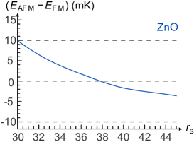
To estimate the typical scale of the spin exchange energy of the Wigner crystal, , we will compare the energy difference per electron of the AFM WC and the FM WC obtained from QMC in Ref. Drummond and Needs, 2009. In Fig. S8 we plot this energy difference in units of mK, by using parameters relevant for ZnO, given by , , as a function of . We also display horizontal dashed lines corresponding to a temperature scale mK. We see that the energy difference never exceeds this temperature scale over the entire range of , and in particular, it is clearly smaller than this scale in the Ferromagnetic side. This suggests that our experimental temperatures are at best only comparable with the scale needed to destroy the spin ordering of the WC at .
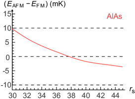
For comparison we plot the same energy difference converted to the scales relevant to AlAs two-dimensional electron systems studied in Ref. Hossain et al., 2020, by taking , in Fig. S9. The value is the geometric mean of the two orthogonal masses. We note that one difference between ZnO and AlAs is the presence of an anisotropic dispersion and multiple valleys of carriers in the latter. By chance the effective unit of energy, , is nearly identical in both settings, ZnO and AlAs, with K. (Here denotes the effective Bohr radius.) For this reason Fig. S8 and Fig. S9 look almost identical.
Since the lowest temperature reached in Ref.Hossain et al., 2020 was mK, it is unlikely that the system reaches the regime of ferromagnetic ordering of the spins of the WC. An alternative explanation for their observations at lowest densities is that the flatness of the magnetoresistance trace as a function of might no longer be a reliable criterion for establishing spin polarization deep in the insulating regime at such elevated temperatures. As we see in our case, even a relatively modest increase of the temperature to about mK, is enough to flatten out the magnetoresistance as a function of at the lowest densities (see e.g. Fig.3c of main text and Fig.S4).
S7 Temperature dependence of the resistance
We divide the data presented in Fig. S10a into separate regimes of temperature in order to perform an analysis of the temperature dependence of the resistance. In this section we first discuss the behavior at zero magnetic field before turning to the behavior at .
S7.1 Zero magnetic field
In electronic insulating phases, the temperature-dependent resistivity is generically described by
| (S15) |
At low temperatures the exponent dominates the behavior of the resistance, and it can take a range of values depending on the mechanism for transport. These include for Arrhenius-type activated transport, for Coulomb-gap mediated variable range hopping, and for Mott-like variable range hopping.Shklovskii and Efros (1984) A common method for estimating the exponent is to perform a Zabrodskii-Zinov’eva analysis, Zabrodskii and Zinov’eva (1984) in which one defines the (dimensionless) reduced activation energy
| (S16) |
The analysis in Fig. S10b suggests that at there exists a regime of at low temperature that crosses over to a regime of at higher temperature, as in conventional semiconductors on the insulating side of the doping-induced metal-insulator transition Shklovskii and Efros (1984). (It is particularly difficult to extract reliable estimates of at mK due to possible decoupling of the electron temperature from that of the cryogen.) Within the regime of , the value of the temperature (which can be called the “Efros-Shklovskii temperature” ) depends on the localization length as Shklovskii and Efros (1984). We observe that vanishes as the electron density approaches from below (Fig. S10c), which is consistent with a divergence of the localization length at the metal-insulator transition.
An alternative and more direct analysis for assessing the temperature dependence of potentially insulating states is to perform a fit to the form of Eq. S15 over all regimes of temperature and density for which (the usual definition of “insulating-like” temperature dependence). Upon close inspection, such a regime appears for all ; it is weak but notable even at our maximum value of under the condition . Figure S11a plots as a function of at a number of at zero magnetic field. The solid lines represent individual fits at discrete . For this process, we avoid using the lowest temperature data points in the strongly insulating regime owing to our inability to exactly determine the electron temperature as the base temperature is approached, and also due to experimental difficulties associated with determining at very low currents in strongly non-linear traces. Figure S11c plots as a function of . The exponent is small (insulating-like behavior is weak) at , but rises rapidly as is reduced below . The value of ultimately appears to saturate at a value of approximately at the lowest .
We separately examine the metallic regime , for which we fit the data according to a power law,
| (S17) |
For this analysis, we restrict the range of temperatures to approximately 16 mk . This is the temperature scaling of the degenerate liquid when . We exclude the lowest temperature data points as we are unable to verify that the electron temperature of the sample is accurately reflected by the thermometer based at the mixing chamber at very low temperatures. Figure S11b presents a log-log plot of the data illustrating a gradually changing slope (i.e. ) as is tuned. The value obtained is plotted as red in Fig. S11c. It can be gauged that is approximately linear in (=1) when 1010 cm-2, with trending towards a value of 1.6 with decreasing immediately before the onset of the MIT. At lower metallicity is rapidly suppressed, and the insulating behavior becomes prominent for all .
S7.2 Evolution with in-plane field
As discussed above, applying an in-plane magnetic field acts to polarize the 2DES into a single spin band. Previous measurements in silicon-based devices have suggested that in-plane field also produces an apparent field-induced MIT at an intermediate partial spin polarization.Shashkin et al. (2001) We examine this effect in Fig. S12 by plotting the longitudinal resistance as a function of at various . Here, we present AC measurements recorded at a current of 2 nA. Panels a-c present the raw magnetotransport data at three distinct . It is possible to identify a change in the sign of at a finite field , at which all the temperature curves coincide. The value of is identified as an open circle in Fig. S12 at both polarities of the field. Tracking the value of as a function of gives the results plotted in panel d. Extrapolating this value to gives a density 1.61010 cm-2 at zero field, which coincides with the value of obtained by DC measurements and discussed in the main text.
In the regime of larger-than-critical density, , and large in-plane field, , the 2DES exhibits insulating-like temperature dependence . However, the form of the temperature dependence in this regime is somewhat weaker than in the regime of discussed above. This weak dependence can be seen in Fig. S12e, which shows that the conductivity increases roughly linearly with temperature (rather than exponentially). Such a linear dependence is qualitatively consistent with a perturbative calculation by Zala et. al. Zala et al. (2001a, b), who found that the conductivity of a spin-polarized FL has a positive, linear-in- correction due to electron-electron interactions. The reduced activation energy in this regime (and at mK) is also consistent with (Fig. S12f).
S8 Disorder-induced density modulation
The phases of the 2DES are generally discussed in terms of a spatially uniform electron density . But when the 2DES is subjected to disorder in the form of stray electric charges, these charges create a random electric potential that modulates the density of the 2DEG spatially. As mentioned in the main text, this modulation allows for the possibility of multiple phases coexisting in different regions of the sample.
A typical source of disorder for a 2DES is a finite concentration of uncontrolled impurity charges embedded three-dimensionally in the substrate. Due to the long-ranged nature of the Coulomb interaction, such impurity charges produce an arbitrarily large variation in the electrostatic potential over sufficiently long length scales, even when their bulk concentration is very small, unless they are screened by the 2DES itself. So long as is sufficiently small (discussed below), this screening can be described using the Thomas-Fermi approximation. Ando et al. (1982) The corresponding root-mean-square variation in electron concentration is given bySkinner and Shklovskii (2013)
| (S18) |
The quantity represents the thermodynamic density of states ( denotes the chemical potential), and can be either positive or negative, depending on the strength of electron correlations. Bello et al. (1981); Eisenstein et al. (1992)
For the strongly-interacting states that we are considering, is of order in magnitude, and consequently
| (S19) |
For our MgZnO/ZnO heterostructures, the bulk impurity concentration is estimated to be below cm-3, Li et al. (2013) so that the corresponding density modulation satisfies
| (S20) |
The Thomas-Fermi approximation that we have employed in this section is valid so long as the typical distance between impurity charges, , is much longer than the Thomas-Fermi screening radius , which in our case amounts to . This inequality is easily satisfied in our devices.
S9 Heating
It is difficult to quantify the extent to which heating influences electrical transport characteristics at very low temperatures. Heating can appear through both current-induced Joule heating (proportional to in an Ohmic system), as well as magnetic processes as the polarity of the applied magnetic field is changed. From our experiences in higher charge density devices ( cm-2) with similar geometries, such as those studied in Refs. [Falson et al., 2015, 2018; Maryenko et al., 2018], Joule heating is negligible in the analysis of fractional quantum Hall energy gaps for currents below approximately 10 nA. However, the charge density, resistivity, and proximity to the MIT of the device under study here puts it in a different parameter space, necessitating a reevaluation of the role of current-induced heating.
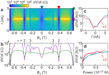
Figure S13 examines the role of current-induced Joule heating by examining transport in the (,)-plane. Panel a renders the differential resistance as a function of perpendicular field and current, with two line cuts being presented in panel b. Integer quantum Hall features are visible as vertical deep blue lines in panel a, and deep minima in panel b. The U-shaped magnetoresistance is evident in the purple trace ( nA), but less so in the finite current trace (green, nA). Conventionally, quantum Hall features exhibit an activated temperature dependence (), where is the activation gap of the state. The depth of the minimum is strongly dependent on temperature, becoming deeper as is reduced. We leverage this character to evaluate the role of current-induced heating. Two traces of as a function of are presented in panel c. The blue trace corresponds to T, with the red trace taken at the minimum T). is chosen in a way that the minimum is finite and should be sensitive to any increase in temperature. The data in panel c shows increases by a factor of approximately three when increasing the current to 5 nA. The data taken at zero field (blue) reveal a notably similar character.
At this charge density (1010 cm-2), reaches 10 k when we heat the mixing chamber to be mK. A heating power approaching 300 W applied to the mixing chamber plate is required in order to achieve that temperature at the thermometer. Panel d takes and plots it as a function of dissipated power across voltage probes (). It is difficult to predict the exact relationship between and power owing to the complicated temperature dependence of the 2DES and thermal coupling of the device to cryogenics surfaces. We remark that the power dissipated inside the samples is 10 orders of magnitude smaller than the equivalent power required at the mixing chamber plate. While our transport measurements preclude detailed conclusions about the texture of carriers inside the device, we speculate that conventional Joule heating of a homogeneous liquid could not be responsible for this increase in .
S10 Methods for determining
The uncertainty involved in the quantification of at very low field values results in deviations in the calculated value of . This uncertainty has quantitative impacts on the results discussed in Fig. 3, but does not change the overall physical picture discussed in this manuscript. For the sake of completeness, here we discuss identification of using three different methods. The second derivative of with respect to exhibits a local minimum in the vicinity of , which can be used to identify its value. This approach may be systematically applied to analyze the data and obtain (). An example of the raw data and second derivative is presented in Fig. S14a. It is visually apparent that the local minimum in occurs at a value of that is close to where the positive magnetoresistance saturates. A second method for estimating is based on fitting a linear slope to in the positive magnetoresistance regime. is defined as the point at which the extrapolated value of this slope is equal to the saturated resistance at high (). An example is displayed in Fig. S14b as the blue trace. Finally, the framework in Ref. [Vitkalov et al., 2001] provides a third method for extracting using the magnetoconductivity data. In this method, is identified with the crossover between a linear fit of and the value at . This third method is demonstrated in Fig. S14b via the red trace.
The results of these three quantification approaches are displayed in Fig. S14c and d. While some systematic discrepancy is evident between the three methods, they each produce the same qualitative features, including: 1) a steady decrease (increase) of () as is reduced from above , 2) an alteration of this trend at approximately , and 3) an apparent saturation of as when .
S11 Temperature and field dependence of excess conductance
The excess conductance identified in Fig. 2 bears some resemblance to other anomalous metal phases discussed in the literature.Kapitulnik et al. (2019) In such systems, the longitudinal resistivity falls at low temperature as if approaching a superconducting ground state, only to saturate at a finite value. This saturation is accompanied by strong positive magnetoresistance. Our results, along with others present in other studies,Kravchenko et al. (1996); Yoon et al. (1999) identify this excess conductance occurring immediately prior to the MIT at zero field. Figure S15 presents an extended data set taken at 1010 cm-2 in the device reported in this work. Panels a and b present at various temperatures as a function of at and 0 T, respectively. A transition from a zero-electric-field insulating state to the excess conductance phase is evident between these two conditions. The former occurs when the 2DES is fully spin polarized, as discussed above. This is clear based on an examination of panel c, where is plotted as a function of , and is seen to saturate above T. Panels d-f map in the (,)–plane at three distinct temperatures. The excess conductance phase is observed at low and as a blue region at low temperature. The insulating phase emerges above and is restricted to low . By mK both of these features are largely washed out.
S12 Two-point current-voltage characteristics
Data presented throughout the main text and previous supplementary information sections have all been gathered in a four-point measurement geometry, as shown in Fig.1a. Figure S16 presents data from the same experimental procedure performed to gather the data of Fig. 2, only taken in a two-point configuration. Here, current is supplied to the device through the sample contacts used to measure the voltage drop, as shown in the upper schematic of Fig. S16. The voltage preamplifier is connected after the load resistor ( M) at the break-out box. The signal therefore contains a contribution from the measurement wires (approximately 150 each direction) and contact resistance of the device. The data in Fig. S16 qualitatively reproduce the result presented in Fig.4 of the main text. The data confirms that the contacts are ohmic for all when mK.