Radio-frequency characterization of a supercurrent transistor made from a carbon nanotube
Abstract
A supercurrent transistor is a superconductor-semiconductor hybrid device in which the Josephson supercurrent is switched on and off using a gate voltage. While such devices have been studied using DC transport, radio-frequency measurements allow for more sensitive and faster experiments. Here a supercurrent transistor made from a carbon nanotube is measured simultaneously via DC conductance and radio-frequency reflectometry. The radio-frequency measurement resolves all the main features of the conductance data across a wide range of bias and gate voltage, and many of these features are seen more clearly. These results are promising for measuring other kinds of hybrid superconducting devices, in particular for detecting the reactive component of the impedance, which a DC measurement can never detect.
I Introduction
When a Josephson junction is fabricated from a semiconductor, its superconducting properties depend on the semiconductor’s density of states. This principle is the basis of the supercurrent transistor Jarillo-Herrero et al. (2006), in which the junction’s critical current is modulated by a nearby gate voltage, allowing the device to be switched between resistive and superconducting states. Supercurrent transistors are components of low-temperature electronics such as SQUID magnetometers Cleuziou et al. (2006) and gatemon qubits Larsen et al. (2015); de Lange et al. (2015). They can be used to measure level crossings Delagrange et al. (2016) and chiral states Szombati et al. (2016) in junctions containing quantum dots, and also to investigate correlated-electron behaviour such as charge localisation Estrada Saldaña et al. (2019).
Josephson junctions based on nanotubes and nanowires have been previously characterised in direct-current (DC) transport Buitelaar et al. (2003); Jarillo-Herrero et al. (2006); Cleuziou et al. (2006). Much greater sensitivity and speed can be achieved using the technique of radio-frequency (RF) reflectometry. Furthermore, DC transport is sensitive only to the conductance of a junction but reflectometry is also sensitive to reactance, and therefore should enable measurements of quantum capacitance Petersson et al. (2010) and Josephson inductance Baumgartner et al. (2020). This has been confirmed by measuring the changes in conductance and inductance associated with the onset of superconductivity in NbTiN/InSb nanowire Josephson junction Pei (2014). The high-frequency impedance of nanowire Josephson junctions has also been investigated by integrating them into on-chip microwave cavities to measure the Andreev states Hays et al. (2018); Tosi et al. (2019); Murani et al. (2019). However, the RF behaviour of a supercurrent transistor, in which the Josephson junction is switched on and off using a gate voltage, has never been investigated.
Here, we use simultaneous RF reflectometry and DC measurements to characterise a supercurrent transistor made of a carbon nanotube. We compare these two methods across the full operating regime of the device in bias and gate voltage. The RF data reproduces all the main features of the DC data, including the onset of superconductivity, a critical current that is tuned by a gate voltage and magnetic field, and the presence of Andreev reflections. In addition, the noise is much lower, as expected for a high-frequency measurement. These results show that a supercurrent transistor can be measured at RF without affecting its operation, and make RF techniques promising for rapidly characterising such devices under a range of conditions.
II Device and Measurement Setup
Supercurrent transistors are fabricated using a single carbon nanotube contacted by superconducting electrodes as shown in figure 1. Device fabrication begins by growing nanotubes on a Si/SiO2 substrate. The nanotubes are grown by chemical vapour deposition using Fe/Ru catalyst nano particles Li et al. (2007) at a temperature of 850 ∘C with methane as the precursor gas Samm et al. (2014). Bondpads and alignment markers are then patterned using electron beam lithography (EBL) and metalized with a bilayer of Ti/Au (10/50 nm). Following lift-off, SEM imaging is used to locate and select individual nanotubes for the transistors. Superconducting source and drain contacts and a gate electrode are then patterned with EBL, developed, cleaned in an ultraviolet ozone chamber, and metallised with a superconducting Pd/Al (4/80 nm) bilayer. The edge-to-edge distance between the contacts is 300 nm. Before mounting the sample, the room-temperature resistances of the devices are measured to check the fabrication yield. Under atmospheric conditions and with the gate floating, roughly 80% of the fabricated devices have a measurable conductance, with typical resistances between 7 k and 100 k. The two devices presented here (Devices A and B) are identical in design and fabrication procedure, but originate from separate fabrication batches, demonstrating the reproducibility of the fabrication.
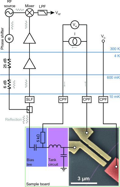
The transistors are measured in the sample puck of a Triton dilution refrigerator with a base temperature between 10 mK and 20 mK, using the circuit shown in figure 1, which allows simultaneous DC and RF measurements and in-situ impedance matching for optimal sensitivity Ares et al. (2016); Schupp et al. (2020). All DC wires are filtered using printed-circuit-board copper powder filters Mueller et al. (2013) containing embedded RC filters. The devices are biased with a source-drain current , and gated using a voltage applied to the side gate. For DC resistance measurements, the voltage at the top of the refrigerator is measured, and converted to a voltage across the device by subtracting the voltage drop across the inline series resistance using
| (1) |
Here is the series resistance, which incorporates all ohmic resistances in the current path, and is determined by a linear fit to the trace in the supercurrent regime. It has the value for Device A (Device B), which is is consistent with the known inline resistance in the cryostat wiring. The differential resistance is calculated numerically.
To allow for RF reflectometry measurements, the device is mounted on a sample board containing an tank circuit and an in-built bias tee made from discrete chip components. The loaded tank circuit exhibits a resonance frequency of 261.2 MHz with a quality factor of about 18. Reflectometry measurements are performed by injecting an RF tone via attenuated coaxial lines and a directional coupler, reflected from the tank circuit, and fed into a homodyne demodulation circuit to generate a demodulated voltage , cf. figure 1. The RF power exciting the tank circuit was approximately dBm. Changes in resistance, capacitance, and inductance of the device modify the phase and amplitude of the reflected signal, and therefore the measured voltage Roschier et al. (2004); Biercuk et al. (2006); Delbecq et al. (2011); Chorley et al. (2012); Ranjan et al. (2015).
III DC spectroscopy
To determine typical properties of the nanotube supercurrent transistor, we first characterized one device (Device A) using only DC measurements. In this measurement, the current bias is applied directly to the bond pad of the source contact, bypassing the bias tee and tank circuit. Figure 2(a) shows the differential resistance as a function of the bias current and gate voltage. This measurement was performed in a gate voltage region more negative than the location of the band gap, i.e. in the -type conduction regime. As expected, we find the critical current is higher in this regime, because the Pd used as contacting layer in the superconducting leads yields a higher transparency of the contacts for holes Chen et al. (2005), i.e. larger . When is close to zero, the differential resistance is small, indicating that the nanotube supports a supercurrent due to the proximity effect. The boundary of this region is marked by a sharp peak in the differential resistance, and is taken as the superconducting critical current .
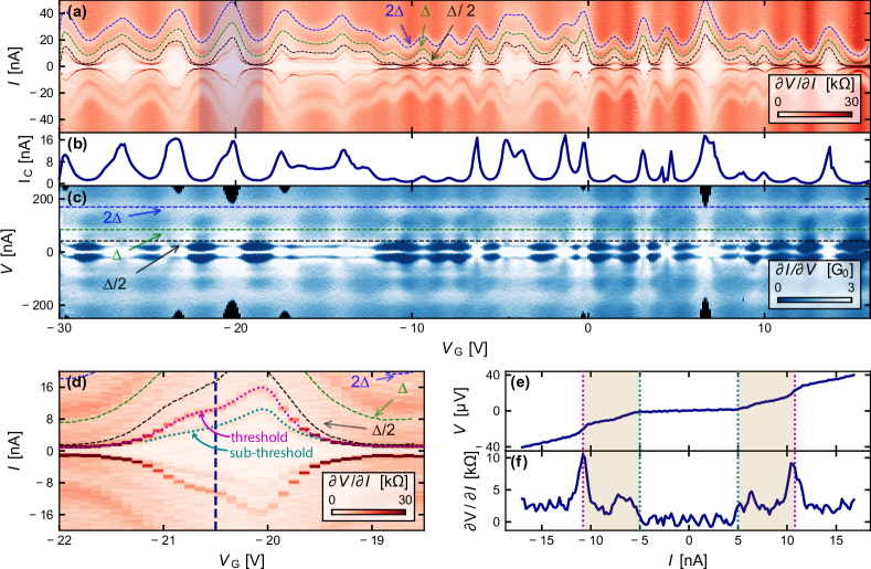
The critical current is strongly modified by changing , as seen from figure 2(b). It ranges from less than 0.1 nA to a maximum of nA. These strong but irregular variations indicate corresponding fluctuations in the nanotube density of states, such as arise from Coulomb blockade or from Fabry-Perot oscillations Jarillo-Herrero et al. (2006). The maximum critical current is higher than in most previous experiments with nanotube junctions Cleuziou et al. (2006); Schneider et al. (2012), although a larger critical current of 30 nA has been achieved using niobium contacts Pallecchi et al. (2008). This is a strong indication of high-transparency contacts between the superconducting leads and the nanotube, and demonstrates the quality of the contact provided by the Al/Pd bi-layer combined with a UV ozone cleaning prior to contact metal deposition. This progress in materials and fabrication methods allows for the integration of such nanotube Josephson junctions into more complex hybrid superconducting devices such as superconducting qubits Mergenthaler et al. (2019). The large measured critical current may also indicate that this quantity depends on the number of walls of the nanotube. We did not measure the wall number or the nanotube diameter in our devices, and it is possible that the nanotube is multi-walled and that this allows for a larger criticial current. The average critical current observed across the full region of covered in figure 2(b) is nA. The fact that depends on confirms that the device is a supercurrent transistor.
For values of greater than , there is a series of broad dips in the differential resistance, consistent with multiple Andreev reflections Nazarov and Blanter (2009); Buitelaar et al. (2003); Jarillo-Herrero et al. (2006). To confirm this interpretation, figure 2(c) shows the same data plotted against the source-drain voltage defined in Eq. (1). As expected, the peaks in conductance occur at voltages
| (2) |
where is an integer and eV (Device A; 95eV, Device B), which is close to the typical value of the superconducting gap in nanotubes contacted with a thin film of aluminium Buitelaar et al. (2003); Jarillo-Herrero et al. (2006). The voltages calculated from equation (2) are marked by dashed lines in figure 2(c) and align with features of low resistance as expected.
Inspection of figure 2(a) also shows weak differential resistance even below the critical current threshold (i.e. for ). Figure 2(d) is an expanded view showing this effect. Two dotted lines highlight the resistance threshold at and this weak sub-threshold feature. Such a sub-threshold resistance indicates excitation away from the superconducting ground state. Two possible causes are thermal phase diffusion and formation of a phase slip Tinkham (1996). Phase diffusion should lead to a smoothly increasing Ambegaokar and Halperin (1969), and phase slips should lead to a series of abrupt steps in Tinkham (1996). The sub-threshold feature in figure 2 does not follow either of these expectations. This is confirmed by figures 2(e-f), which plot and along a single cross-section in bias current. We therefore tentatively suggest that the sub-threshold peak in indicates that the device contains two weak links in series, and that the sub-threshold peak occurs when the weaker of the two becomes normal. This might happen if the interface on one side of the device is less clean than on the other. If this is the correct explanation, then the value of plotted in figure 2(c) is the critical current of the stronger link. This sub-threshold peak is not observed in Device B (see below). However, we note that a similar peak has been seen just below the transition temperature in a NbN nanowire device that also exhibited thermal and quantum phase slips Masuda et al. (2016).
IV Spectroscopy using RF reflectometry
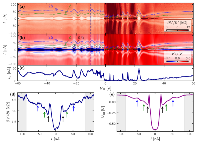
Reflectometry experiments were performed on a second device (Device B) fabricated by a similar method as Device A but in a separate fabrication run. Device B was bonded to the sample board in the same way as Device A (figure 1) but now with the tank circuit connected. The measurement of figure 2(a) was now repeated, except that as well as the DC conductance , the demodulated RF voltage was measured simultaneously. The integration time per point was the same for the two data sets.
Figure 3(a)-(c) shows the results. As expected, the DC behaviour (figure 3(a)) is similar to figure 2(a), which confirms that the supercurrent transistor can operate with an RF excitation applied. All the main features are reproduced in the RF measurement (figure 3(a)), especially the sharp change at the critical current. We find that is approximately proportional to the DC resistance, showing that the RF measurement successfully transduces changes in the device impedance into changes in the tank circuit’s reflectance.
Some features of the DC resistance appear more clearly in the RF data, in particular the sharp superconducting transition. To explore this more thoroughly, figure 3(d) and figure 3(e) compare cross-sections at constant V, which is a typical gate voltage in the transistor’s ‘On’ configuration. The superconducting transition and the first two Andreev features are evident in the conductance data (figure 3(d)) but much clearer in the reflectometry data (figure 3(e)). The signal-to-noise ratio is higher for the RF measurement. Quantifying the noise as the scatter of the data points in the quasiparticle transport regime, and the signal as the full vertical range of the traces in figure 3, the RF measurement yields an improvement of dB. This illustrates the advantage of measuring at an RF frequency where noise is reduced compared with DC. It may also indicate that part of the RF signal is a response to the changing superconducting inductance, to which the DC measurement is insensitive.
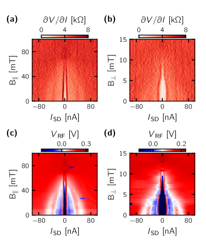
As a further illustration of the sensitivity of RF measurement, figure 4 shows the DC differential resistance and the RF signal as a function of magnetic field applied in (B∥) and out of plane (B⟂) of the device substrate. As expected, the critical current decreases with increasing field, an effect that is seen more clearly in the RF than in the DC measurement.
V Conclusion
By comparing simultaneous RF and DC transport measurements of a carbon nanotube supercurrent transistor, this experiment shows that RF reflectometry is sensitive to all the main transport features, most of which appear more distinctly than in DC transport alone. Importantly, the properties of a supercurrent transistor device integrated into an RF measurement circuit are essentially identical to those of a device measured by DC transport alone. Our results show that RF reflectometry is a non-invasive technique for characterising supercurrent transistors and potentially many other nanoscale devices and physical effects. Although not tested here, reflectometry measurements can often be much faster than transport alone, and thus may allow many devices to be tested quickly under a wide range of operating conditions. This would allow, for example, rapid fluctuations of the critical current to be measured in real time Rogers and Buhrman (1983). The reflectometry circuit used here might also allow for fast testing of other kinds of superconducting hybrid devices, for example to compare different ways of optimising superconductor-semiconductor interfaces, which are crucial for such devices. The ability to distinguish reactive and resistive impedance changes is a possible tool for studying novel hybrid devices such as those used to realise Majorana qubits Aguado and Kouwenhoven (2020); Smith et al. (2020).
Acknowledgements.
We acknowledge support from the Royal Academy of Engineering, EPSRC (EP/R029229/1), the ERC (818751), the Swiss Nanoscience Institute (SNI) and the Swiss National Science Foundation. M. M. acknowledges support from the Stiftung der Deutschen Wirtschaft (sdw). We thank Yu. A. Pashkin for discussions.References
- Jarillo-Herrero et al. (2006) P. Jarillo-Herrero, J. A. van Dam, and L. P. Kouwenhoven, Nature 439, 953 (2006).
- Cleuziou et al. (2006) J.-P. Cleuziou, W. Wernsdorfer, V. Bouchiat, T. Ondarçuhu, and M. Monthioux, Nature Nanotechnology 1, 53 (2006).
- Larsen et al. (2015) T. W. Larsen, K. D. Petersson, F. Kuemmeth, T. Jespersen, P. Krogstrup, J. Nygård, and C. Marcus, Physical Review Letters 115, 127001 (2015).
- de Lange et al. (2015) G. de Lange, B. van Heck, A. Bruno, D. J. van Woerkom, A. Geresdi, S. R. Plissard, E. P. A. M. Bakkers, A. R. Akhmerov, and L. DiCarlo, Physical Review Letters 115, 127002 (2015).
- Delagrange et al. (2016) R. Delagrange, R. Weil, A. Kasumov, M. Ferrier, H. Bouchiat, and R. Deblock, Physical Review B 93, 195437 (2016).
- Szombati et al. (2016) D. B. Szombati, S. Nadj-Perge, D. Car, S. R. Plissard, E. P. Bakkers, and L. P. Kouwenhoven, Nature Physics 12, 568 (2016).
- Estrada Saldaña et al. (2019) J. C. Estrada Saldaña, R. Žitko, J. P. Cleuziou, E. J. Lee, V. Zannier, D. Ercolani, L. Sorba, R. Aguado, and S. De Franceschi, Science Advances 5, eaav1235 (2019).
- Buitelaar et al. (2003) M. R. Buitelaar, W. Belzig, T. Nussbaumer, B. Babić, C. Bruder, and C. Schönenberger, Physical Review Letters 91, 057005 (2003).
- Petersson et al. (2010) K. D. Petersson, C. G. Smith, D. Anderson, P. Atkinson, G. A. C. Jones, and D. A. Ritchie, Nano Letters 10, 2789 (2010).
- Baumgartner et al. (2020) C. Baumgartner, L. Fuchs, L. Frész, S. Reinhardt, S. Gronin, G. C. Gardner, M. J. Manfra, N. Paradiso, and C. Strunk, Physical Review Letters 126, 037001 (2020).
- Pei (2014) F. Pei, Quantum transport in one-dimensional nanostructures, Ph.D. thesis, TU Delft (2014).
- Hays et al. (2018) M. Hays, G. de Lange, K. Serniak, D. van Woerkom, D. Bouman, P. Krogstrup, J. Nygård, A. Geresdi, and M. Devoret, Physical Review Letters 121, 047001 (2018).
- Tosi et al. (2019) L. Tosi, C. Metzger, M. F. Goffman, C. Urbina, H. Pothier, S. Park, A. L. Yeyati, J. Nygård, and P. Krogstrup, Physical Review X 9, 11010 (2019).
- Murani et al. (2019) A. Murani, B. Dassonneville, A. Kasumov, J. Basset, M. Ferrier, R. Deblock, S. Guéron, and H. Bouchiat, Physical Review Letters 122, 076802 (2019).
- Li et al. (2007) X. Li, X. Tu, S. Zaric, K. Welsher, S. S. Won, W. Zhao, and H. Dai, J. Am. Chem. Soc. 129, 15770 (2007).
- Samm et al. (2014) J. Samm, J. Gramich, A. Baumgartner, M. Weiss, and C. Schönenberger, J. Appl. Phys. 115, 174309 (2014).
- Ares et al. (2016) N. Ares, F. Schupp, A. Mavalankar, G. Rogers, J. Griffiths, G. Jones, I. Farrer, D. Ritchie, C. Smith, A. Cottet, G. Briggs, and E. Laird, Physical Review Applied 5, 034011 (2016).
- Schupp et al. (2020) F. J. Schupp, F. Vigneau, Y. Wen, A. Mavalankar, J. Griffiths, G. A. C. Jones, I. Farrer, D. A. Ritchie, C. G. Smith, L. C. Camenzind, L. Yu, D. M. Zumbühl, G. A. D. Briggs, N. Ares, and E. A. Laird, Journal of Applied Physics 127, 244503 (2020).
- Mueller et al. (2013) F. Mueller, R. N. Schouten, M. Brauns, T. Gang, W. H. Lim, N. S. Lai, A. S. Dzurak, W. G. van der Wiel, and F. Zwanenburg, Review of Scientific Instruments 84, 044706 (2013).
- Roschier et al. (2004) L. Roschier, M. Sillanpää, W. Taihong, M. Ahlskog, S. Iijima, and P. Hakonen, Journal of Low Temperature Physics 136, 465 (2004).
- Biercuk et al. (2006) M. J. Biercuk, D. J. Reilly, T. M. Buehler, V. C. Chan, J. M. Chow, R. G. Clark, and C. M. Marcus, Physical Review B 73, 201402 (2006).
- Delbecq et al. (2011) M. R. Delbecq, V. Schmitt, F. D. Parmentier, N. Roch, J. J. Viennot, G. Fève, B. Huard, C. Mora, A. Cottet, and T. Kontos, Physical Review Letters 107, 256804 (2011).
- Chorley et al. (2012) S. J. Chorley, J. Wabnig, Z. V. Penfold-Fitch, K. D. Petersson, J. Frake, C. G. Smith, and M. R. Buitelaar, Physical Review Letters 108, 036802 (2012).
- Ranjan et al. (2015) V. Ranjan, G. Puebla-Hellmann, M. Jung, T. Hasler, A. Nunnenkamp, M. Muoth, C. Hierold, A. Wallraff, and C. Schönenberger, Nature Communications 6, 7165 (2015).
- Chen et al. (2005) Z. Chen, J. Appenzeller, J. Knoch, Y.-m. Lin, and P. Avouris, Nano Letters 5, 1497 (2005).
- Schneider et al. (2012) B. H. Schneider, S. Etaki, H. S. J. van der Zant, and G. A. Steele, Scientific Reports 2, 599 (2012).
- Pallecchi et al. (2008) E. Pallecchi, M. Gaaß, D. A. Ryndyk, and C. Strunk, Applied Physics Letters 93, 072501 (2008).
- Mergenthaler et al. (2019) M. Mergenthaler, A. Nersisyan, A. Patterson, M. Esposito, A. Baumgartner, C. Schönenberger, G. A. D. Briggs, E. A. Laird, and P. J. Leek, “Realization of a Carbon-Nanotube-Based Superconducting Qubit,” (2019), arxiv/1904.10132 .
- Nazarov and Blanter (2009) Y. V. Nazarov and Y. M. Blanter, Quantum Transport: Introduction to Nanoscience (Cambridge University Press, 2009).
- Tinkham (1996) M. Tinkham, Introduction to Superconductivity, 2nd ed. (McGraw-Hill, New York, 1996).
- Ambegaokar and Halperin (1969) V. Ambegaokar and B. I. Halperin, Physical Review Letters 22, 1364 (1969).
- Masuda et al. (2016) K. Masuda, S. Moriyama, Y. Morita, K. Komatsu, T. Takagi, T. Hashimoto, N. Miki, T. Tanabe, and H. Maki, Applied Physics Letters 108, 222601 (2016).
- Rogers and Buhrman (1983) C. Rogers and R. Buhrman, IEEE Transactions on Magnetics 19, 453 (1983).
- Aguado and Kouwenhoven (2020) R. Aguado and L. P. Kouwenhoven, Physics Today 73, 44 (2020).
- Smith et al. (2020) T. B. Smith, M. C. Cassidy, D. J. Reilly, S. D. Bartlett, and A. L. Grimsmo, PRX Quantum 1, 020313 (2020).