Enhanced on-chip frequency measurement using weak value amplification
Abstract
We present an integrated design to precisely measure optical frequency using weak value amplification with a multi-mode interferometer. The technique involves introducing a weak perturbation to the system and then post-selecting the data in such a way that the signal is amplified without amplifying the technical noise, as has previously been demonstrated in a free-space setup. We demonstrate the advantages of a Bragg grating with two band gaps for obtaining simultaneous, stable high transmission and high dispersion. We numerically model the interferometer in order to demonstrate the amplification effect. The device is shown to have advantages over both the free-space implementation and other methods of measuring optical frequency on a chip, such as an integrated Mach-Zehnder interferometer.
I Introduction
Weak value amplification (WVA) [1, 2, 3] can be used to amplify small parameters without amplifying certain types of technical noise, in order to obtain a higher signal-to-noise ratio [4]. The technique has been used to obtain enhanced measurements of a variety of parameters, such as the angular deflection of a mirror [5, 6], beam displacements [7], and temperature changes [8]. Here, we propose an integrated interferometer design that uses WVA to sensitively measure changes in optical frequency.
There are many different types of sensors that have been developed to precisely measure the frequency of a laser [9, 10, 11, 12, 13, 14]. This particular design is inspired by a previous experiment using free space optics [15], but is implemented in an integrated optics environment. The design is a multi-mode Mach-Zehnder interferometer (MZI) [16, 17] with a small mode perturbation which is coupled to the relative phase between arms. The output power is sorted such that all the information content is concentrated into a small fraction of the light, giving full precision with less light reaching the detector. This allows us to use a much higher input power without saturating the detector. The power that does not reach the detector can be discarded, used as a reference, or recycled [18, 19], which could allow for better precision. Using this design, we set a fundamental precision limit of using readily achievable waveguide parameters and of detected power ( of input power), and show that this is better than the precision given by an equivalent standard MZI [20].
Integrated optics makes a nice platform for miniaturizing interferometers. It has been proposed for making a series of interferometers as needed in boson sampling experiments [21], and for single interferometers such as the integrated Sagnac interferometer [22, 23]. These integrated interferometers have a wide range of applications, including gyroscopes and accelerometers [24, 25, 26, 27]. Using an integrated optics platform automatically stabilizes the interferometer from drifts in mirror position or air currents, and makes it easier to parallelize the sensing system. Another advantage of working on a chip is that it is possible to implement high-efficiency avalanche photodetectors using nanophotonic techniques [28].The low noise properties of these detectors enable detection of weak optical signals at very high speed.
This paper is organized as follows. In Section II, we lay out the integrated interferometer design and demonstrate the WVA effect, using theory and numerical simulations. In Section III, we study the dispersive element of the interferometer, and discuss the advantages of using a Bragg grating with two band gaps. In Section IV, we calculate the precision of the device using Fisher information and quantify the advantage over a MZI. In Section V, we discuss several common error types that can arise in this kind of interferometer, and show that our WVA design reduces the effect of certain errors compared to a MZI. We conclude in Section VI.
II Interferometer design
II.1 Background
Weak value amplification consists of three steps: (1) pre-selection, where the system is prepared in an initial state; (2) a weak perturbation to the system state; and (3) post-selection, where the system is projected onto a final state, which is chosen to be nearly orthogonal to the initial state. The result is that only a small fraction of the data is retained, but that small fraction contains nearly the entire information content about the parameter being measured. Consequently, we can use more input power for better precision without saturating the detector.
We consider an infinite planar dielectric waveguide where the core, with index of refraction , exists everywhere in space for . The cladding layers fill the remainder of space, and for simplicity we assume they both have the same index of refraction , where so that the wave is guided. We take the -direction to be the direction of propagation and assume , where is any component of the field. We make use of the first two transverse electric modes and (although a similar analysis can be applied to the TM modes). The first two TE modes are
| (1) |
| (2) |
where are transverse wavenumbers, are decay constants, and are the propagation constants associated with the two modes [29]. The amplitudes are given by and , where are determined by normalization. The propagation constants can be determined by solving the transcendental equation
| (3) |
where labels the modes. For this design, we choose waveguide parameters such that there are only two solutions, corresponding to . The highest supported guided modes is the number for which
| (4) |
so we choose parameters such that this inequality is satisfied when . For numerical simulations throughout this paper, we choose , , and indices of refraction and , corresponding to a silicon nitride core and silica cladding [30].
II.2 Pre-selection
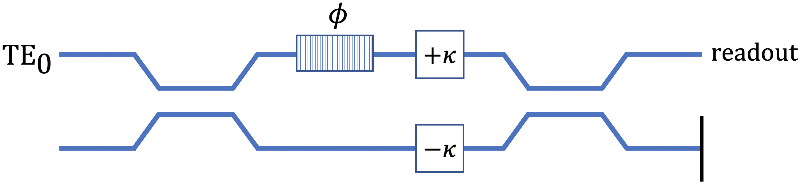
We propose an interferometer design, shown in Fig. 1, which uses a small mode perturbation to sensitively read out the optical frequency of the input beam. We start with an injected mode in the upper arm, which can be represented in the joint space as
| (5) |
where the path vector refers to the two arms of the interferometer in the (upper, lower) basis, and the mode vector is in the (, ) basis. This state is split with a 50/50 directional coupler, which uses evanescent coupling to transfer power between the two waveguides. The power in the upper and lower waveguides during the directional coupler is
| (6) |
where is a coupling constant [31]. To obtain a coupler, we choose the length of the coupler to be , resulting in
| (7) |
In one of the arms, the light encounters a dispersive medium, such as a Bragg grating, that imparts a frequency-dependent phase . The grating has a medium index that depends sharply on the frequency, resulting in a steep dispersion relation. This is discussed further in Section III. The state picks up a relative phase between the two arms that depends sensitively on the optical frequency,
| (8) |
II.3 Mode perturbation
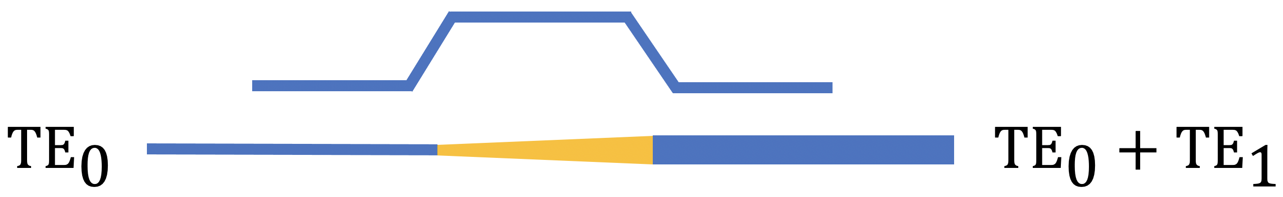
After introducing the relative phase, we apply opposite tilted phase fronts with wavenumber (where is taken to be real) by converting a small fraction of the mode into . The opposite change can be engineered across the other waveguide. We present a design for a “mode converter”, shown in Fig. 2, in order to perform the transformation
| (9) |
where opposite signs are used in each arm. This is similar to the transformation caused by a beam splitter, but in mode space. It is analogous to the beam deflection caused by a prism or mirror tilt in the free space setup [15, 5]. The parameter should be chosen such that in order to realize the weak value effect. The state after the mode perturbation, written as a non-separable vector in the same basis, is
| (10) |
II.4 Post-selection
The light in the two arms of the interferometer is then combined using another directional coupler. The and modes have different coupling constants , so we must be careful to choose a length where both modes have transferred half their power. After this directional coupler, the state is
| (11) |
The upper and lower arms have total intensity (normalized relative to the input intensity)
| (12) |
where , so we refer to the corresponding output ports as the “dark port” and “bright port” respectively. We post-select on the dark port, which gives the state
| (13) |
to first order in the approximations and . If we are interested in measuring the carrier frequency via the phase, then we can rewrite the mode as
| (14) |
so after renormalization, we have mainly a mode with a small amount of mode added in. The phase is “amplified” by , and the post-selection probability is given by .
We suggest two different methods to read out the amplified phase. One method is to measure the ratio between and modes, giving a signal
| (15) |
This mode ratio can be read out using a separate multi-mode interferometer at the dark port which has an output power that depends on the mode ratio. It could also be read out by bringing in a new waveguide, whose fundamental mode frequency is equivalent to the mode of the original waveguide, and which will not support the original mode. In this way, we can siphon off the mode while leaving the mode untouched. Photodetectors would then be placed at the ends of those waveguides, and the relative intensity would be read out. Applied to the case of mode (14), one detector would collect only the information signal, and register intensity , while the other would measure intensity , which would carry no frequency information. The latter signal can be monitored as a reference, discarded, or recycled [18, 19]. As is shown in Section IV, measuring the mode ratio is an optimal measurement, i.e. it gives the best possible frequency precision. This is amplified by a factor of when compared with the standard MZI signal, , derived by taking the intensity difference between the two output ports.
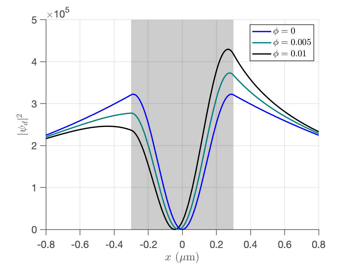
A second readout method is to measure the displacement of the mode profile. This is a closer analogy with free space experiments, where the phase is read out by measuring the beam deflection with a split detector. In this case, the expectation value of the transverse position in the dark port depends on the amplified phase,
| (16) |
The intensity profile is shown for various values of in Fig. 3. This could be measured using a Y-branch in the waveguide, terminated at the end of the sample by fast photodiodes. The normalized difference signal from the photodiodes in the two arms is
| (17) |
where and are the intensities in the left and right half of the dark port waveguide, and is a mode constant which does not depend on or . Unlike the mode ratio method, this readout scheme is not optimal, meaning it cannot saturate the ultimate bound on frequency precision (this is discussed further in Section IV). Also, the true value of diverges more quickly from the linear approximation we have used, leading to a smaller working range in . For these reasons, we will use the mode ratio readout throughout the rest of this paper.
III Slow light using a double Bragg grating
III.1 Bragg grating theory
In order to create strong dispersion, we consider the use of a Bragg grating in one arm of the interferometer [29, 34]. Another method of creating a frequency-dependent phase is to use the dispersion provided by one or more ring resonators [35], but here we restrict the analysis to Bragg gratings. A Bragg grating is a periodic alternating index of refraction
| (18) |
where is the effective index of refraction of the waveguide for the mode (the only mode traveling through the grating), and has spatial periodicity . The periodic grating opens a photonic band gap, where certain wavenumbers cannot propagate through the grating, centered at . This is analogous to the conduction band gap in semiconductors. The traveling waves exhibit dispersion, and slow light effects can appear near the band gap. This is related to the nonvanishing first derivative of the index of refraction with respect to frequency. While any periodic index of refraction is sufficient to produce this effect, we will focus here on the simplest case of a sinusoidal grating, , which can be created using laser etching from an interference pattern as one fabrication technique.
For a Bragg grating of infinite length, the propagating field takes the form , where
| (19) |
is the new wavenumber, is the detuning of the wavenumber from the Bragg wavenumber , and is the coupling coefficient between the forward and backwards modes. If the detuning is less than the coupling , there is no (real) solution, and the traveling wave mode cannot exist. Outside this band, the wave number is modified by the grating to become . The dependence of on indicates the presence of dispersive effects. We expand in a Taylor series in ,
| (20) |
and study the first derivative, which sets the group velocity of the grating (or sensitivity of the phase to frequency),
| (21) |
where is the native group velocity of the waveguide. As approaches , the group velocity slows to zero, while for , the grating is irrelevant.
The group velocity of a finite-length grating can be obtained using
| (22) |
where
| (23) |
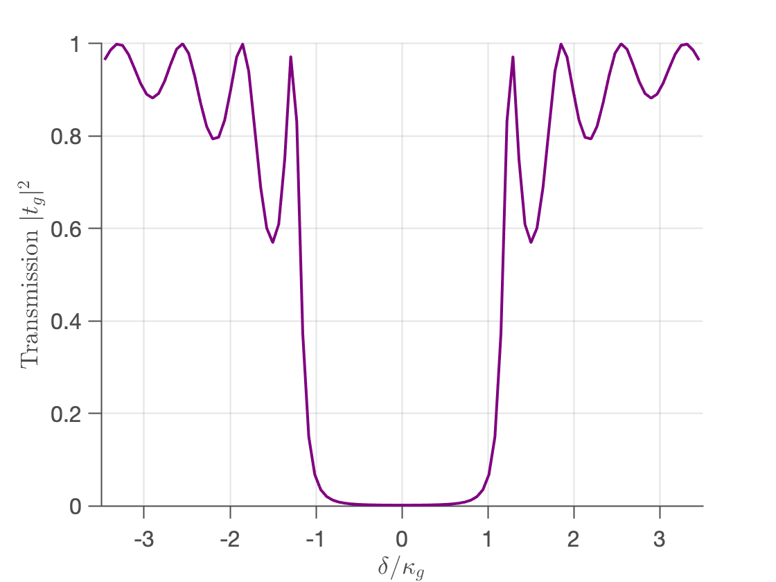
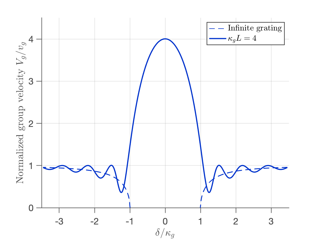
is the complex reflection coefficient [36, 37]. This takes into account edge effects, which cause oscillations about the expression given in (21). Equation (22) converges to (21) as the length of the grating becomes very large. A comparison is shown in Fig. 4.
While it may be tempting to work very close to to get the slowest light, this is generally a bad idea because a large fraction of the light is reflected. Fig. 4 demonstrates the inconvenient conclusion that when the group velocity is low, the transmission is also low. If we move a bit away from and take the length of the grating to be fairly long, we can still obtain high transmission while keeping relatively low group velocity.
One of the awkward features of working near the band gap is that while there is dispersion that will help in our frequency measurement, the transmission is changing (typically rapidly) as frequency (or detuning) is changed, as shown in Fig. 4. We would like to have relatively constant transmission throughout the working frequency range, while also having small group velocity, or high dispersion.
III.2 Two resonances
One way to mitigate this difficulty that was proposed in the context of atomic resonances is to work in the region between two resonances [38, 39]. This technique allows high-precision frequency measurements with relatively high optical transmission so as to minimize the optical losses. We can use an analogous idea here by having a double periodicity in the grating,
| (24) |
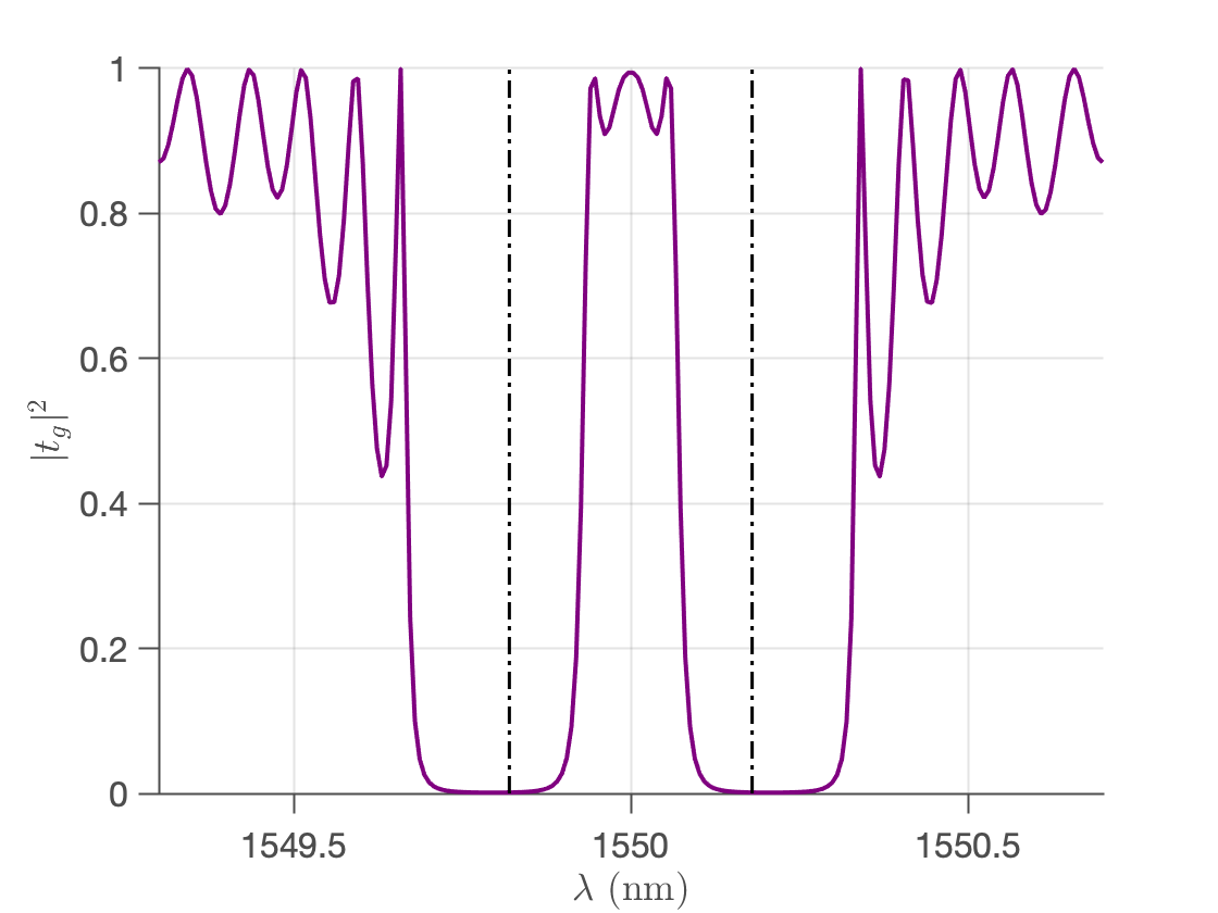
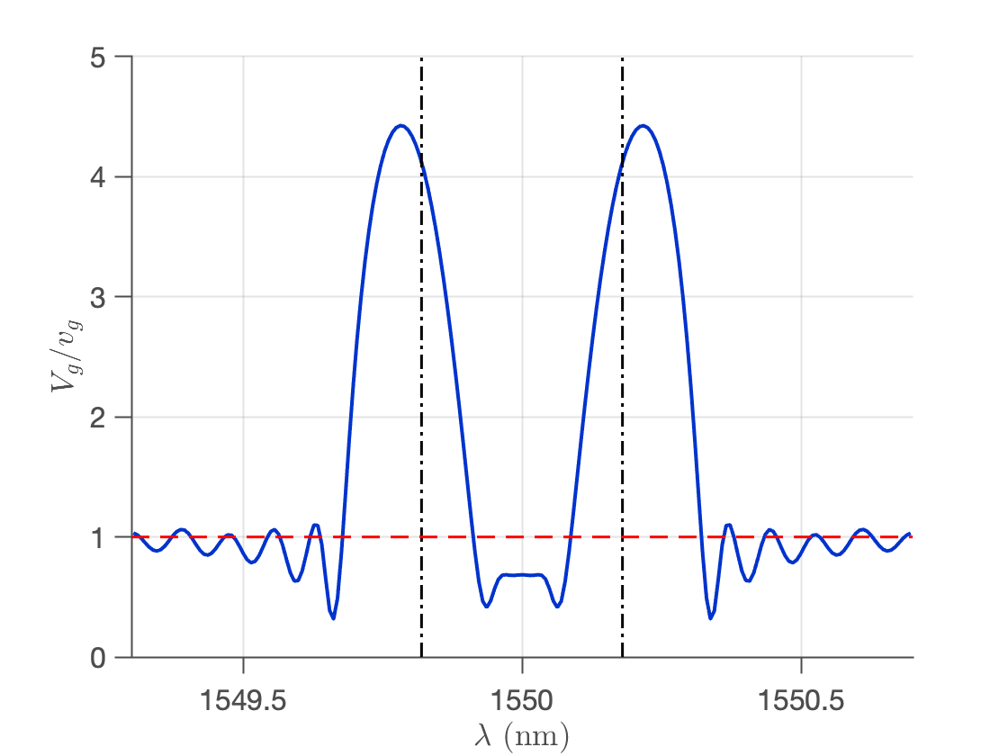
This grating will then open up two photonic band gaps centered at and , each with a width given by , where and . By arranging a region of parameter space that allows propagating modes between and , we can accomplish the same basic physics that was accomplished in the atomic system: a region of frequency space that has fairly high transmission, but also high dispersion (very slow light). A numerically simulated comparison of transmission and group velocity for a grating with two band gaps is shown in Fig. 5. As expected, there are two band gaps centered at and . The regions inside the band gaps exhibit superluminal group velocity but close to zero transmission. On the outside of the two band gaps, the transmission and group velocity both oscillate. In the center of the two band gaps, there is high transmission and relatively low group velocity, which are the desired qualities of the double Bragg grating concept design. The region between the band gaps is small (in Fig. 5 the window is ) which limits the working frequency range, but the whole region has high transmission and low group velocity.
IV Sensitivity and precision analysis
IV.1 Sensitivity
The frequency sensitivity of the device is given by
| (25) |
where is the output signal given by (15) or (17) depending on the readout method, is the dispersion from the Bragg grating, is the frequency shift to be measured, and is the amplification factor using the mode ratio readout method. The higher the dispersion and amplification of the device, the more sensitive the signal will be to changes in frequency. The relative phase caused by the Bragg grating, assuming equal path lengths, is given by , so the dispersion is given by
| (26) |
Using (so that ), , and (which was obtained numerically using the chosen waveguide parameters), the overall sensitivity is
| (27) |
For example, if , this is . Compare this to a MZI, which has , resulting in a sensitivity of . The WVA interferometer results in a sensitivity that is enhanced by the amplification factor .
IV.2 Precision
The Cramér-Rao bound (CRB) gives the fundamental limit on the precision of a parameter being estimated [40]. In this case, it gives the minimum detectable change in frequency,
| (28) |
where is the Fisher information,
| (29) |
and and are the probabilities of the two measurement outcomes. For a standard MZI [20], a photon can arrive at one of two output ports, with probabilities and , resulting in the minimum detectable frequency change
| (30) |
for total input photons. The frequency sensitivity depends on the input power and the dispersion . For an input power of , this gives a precision bound of . This value depends heavily on the dispersion provided by the Bragg grating.
For the WVA interferometer, we only look at the dark port (which detects no photons when ), and use the mode ratio to make a measurement. The probabilities associated with the and modes are and . The Cramér-Rao bound in this case is the same as for the MZI, despite only using a small fraction of the available power. The low detection probability is balanced by the amplification of , which concentrates the Fisher information into the subset of data being measured. The advantage of the WVA interferometer lies in the fact that we can greatly increase the number of photons without overloading the detector, since most of the input light never reaches the detector. If we increase , the minimum detectable frequency change is
| (31) |
which is decreased by a factor of . We have increased the amount of input power to achieve better precision, but critically, the amount of power arriving at the detector is the same as it is for a MZI. With , we can use times as much input power, so the precision bound is .
IV.3 Quantum Fisher information
When doing parameter estimation using a quantum state, the quantum Fisher information (QFI) gives an upper bound on the Fisher information optimized over all possible measurement schemes [40]. The QFI for the output of the WVA interferometer, including both ports, is . This is the maximum possible information that can be gained from the readout. This information is almost entirely concentrated into the dark port, which can be seen by calculating the QFI for the dark port only, . As , this approaches the total QFI contained in the system. This means in the limit, the WVA interferometer channels almost all the information in the system into the dark port, even though it contains only a small fraction of the input power.
An optimal measurement will be one whose Fisher information saturates the QFI. If we consider the mode ratio readout method, the Fisher information is , as in (30). In this case , so reading out the mode ratio is an optimal measurement. If instead we read out the mode displacement as in (17), we can treat and take , to obtain the Fisher information
| (32) |
In this case , which means this is not an optimal measurement scheme. Using the chosen waveguide parameters, , which results in a precision loss by a factor of only compared to the mode ratio method, so it could still be worth using if it is easier to implement experimentally.
V Error analysis
Some of the main errors and sensitivities that affect interferometers are: (1) bias offset error, (2) bias instability, (3) temperature sensitivity, and (4) shock and vibration sensitivity [41, 42]. Bias offset error is the systematic error that the instrument shows when it is at rest. Typically this constant meter reading is a product of fabrication and can be subtracted off in the calibration process. The bias instability, however, corresponds to a relatively slow random walk in the bias offset, which leads to slow random error, which will limit the accuracy of the sensor. In the subsections that follow, we make an analysis and simulation of errors (1), (2), and (3). Error (4) is difficult to simulate because the error source is not the system itself, but rather the detector electronics and aspects outside the interferometer. It is therefore more accurately measured in the experimental testing of the device. Also, the integrated optical readout greatly reduces shock and vibration sensitivity compared to the free space version. Unless the integrated optical semiconductor structure itself is shattered or severely deformed, this will not be relevant.
We expect that WVA techniques will help in three ways. First, the systematic bias offset in the meter reading will be suppressed compared to a MZI, provided that source of the drift is outside the system itself. Second, even if the offset drifts, as expected in the bias instability noise induced by the detector and surrounding environment, the WVA will also suppress it, even if it is unknown. Third, and perhaps most importantly, the fact that standard commercial detectors saturate after a few tens of mW of power allows us to use much higher input power, and even though the detectors measures only a fraction of that power, we attain a precision equal to that of the entire input power, giving an important practical advantage.
V.1 Bias offset errors
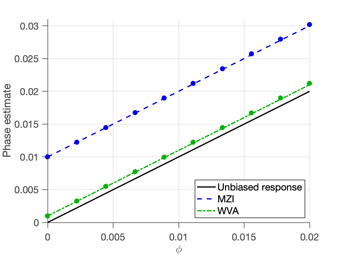
The phase readout can be biased if there are slight imperfections in the interferometer components. This bias could also come from slightly imbalanced loss in the two waveguides leading to the detector, or any number of other possible asymmetries in the system. In practice, this means the device will detect a frequency that is different from the true frequency by some constant offset. In the WVA interferometer, the frequency readout is amplified while the bias offset error is not, so the error is suppressed [43].
We can model a bias offset error as a certain fraction of photons being misread by the detector. In a MZI, where the signal is given by the difference between the lower and upper waveguide intensities , we add in a bias by supposing the detector misreads a fraction of the upper waveguide photons as being in the lower waveguide, . This results in the phase estimate being , where the phase offset is . In the WVA interferometer, the signal is given by the mode ratio in the dark port, so we similarly define the bias offset error to be a fraction of photons in being detected as if they were in . This results in a signal , where we have assumed to get a linear offset. The phase offset in this case is , which has been suppressed by a factor of . The suppression of a bias offset error by the WVA effect is shown in Fig. 6.
The offset discussed here is easy to subtract off and calibrate away, so long as it does not drift in time. We will discuss the case of the drifting offset in the next subsection. The interferometer can be calibrated by measuring the phase offset when , and then accounting for this bias in any future measurements.
V.2 Bias instability
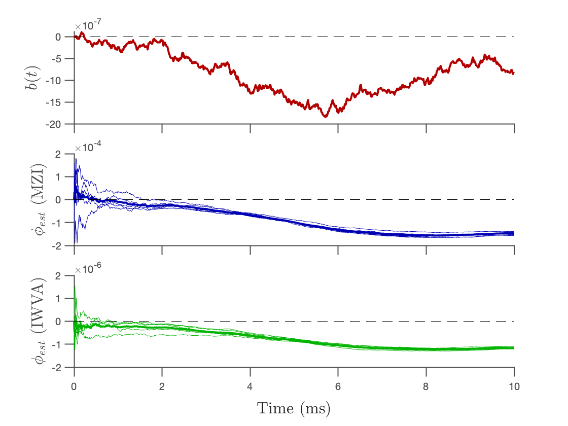
Bias in the interferometer is more difficult to deal with when it varies in time. If the bias factor is time-dependent, the readout signal , and therefore the phase estimate , will depend on the time-averaged bias factor . We suppose that we can calibrate away the constant offset from the fabrication of the device, and only have to contend with the time-varying bias instability. We model the bias instability as a random walk in the bias offset, where is a normally distributed random variable with mean and standard deviation . This number is typical of what we expect from thermal drifts.
The drifting bias offset causes a corresponding drift in the phase offset , and we know from the previous section that for the MZI and for WVA. The standard deviation of the drift in phase offset for the same amplitude and time scale of the bias instability is then for the MZI, and is suppressed to for the WVA with . The sum of detected signals for a MZI and the WVA interferometer (using the mode displacement readout technique for closer analogy with the MZI signal) under influence of such a bias offset is shown in Fig. 7. As with the constant bias offset, this suppression can be enhanced by increasing the amplification in the WVA interferometer.
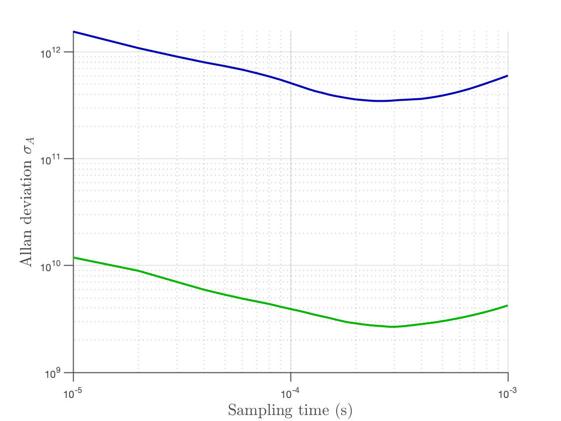
To quantify the advantage of this method, we compute the Allan variance of the MZI and the WVA interferometer [41, 42, 44]. The Allan variance is a measure of how quickly the rate of an accumulating signal is changing. It is calculated by grouping a sequence of data points into time bins of length , and using
| (33) |
The Allan variance is generally minimized over the sampling time . If the bias is very unstable, the signal will change by very different amounts over each sampling time, and the Allan variance (and Allan deviation ) will be large. A comparison of the Allan deviation for MZI and WVA is in Fig. 8, which confirms that the effect of bias instability is greatly reduced by the WVA effect.
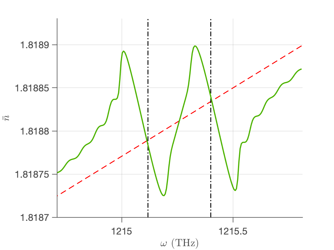
V.3 Thermal effects
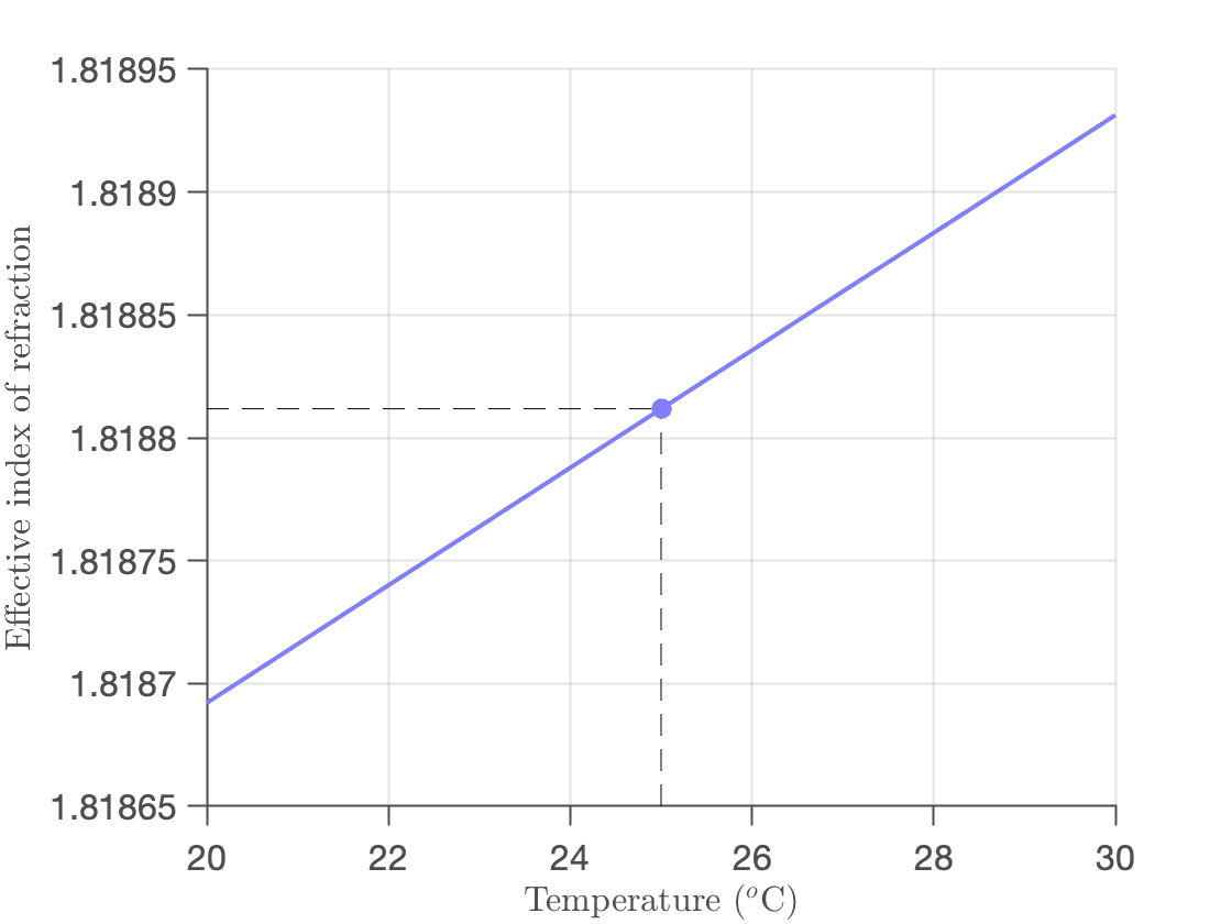
The temperature stability of the sensor is affected by the thermally dependent index of refraction of the waveguide materials. On one hand, this is helpful because heaters can be placed near the waveguides in order to fine tune their optical properties. On the other hand, undesired temperature shifts can create systematic errors in the accuracy of the measurement readings. We quantify this behavior using the thermo-optic effect in our materials of choice (Si3N4 for the core and SiO2 for the cladding),
| (34) |
where is the temperature [45]. The propagation of the mode through the waveguide is described by the effective index of refraction , which was determined numerically using the chosen waveguide parameters and the techniques laid out in Section II. The effective thermo-optic coefficient is determined in Fig. 9 to be . The same argument also applies to , which will have a different effective thermo-optic coefficient, . The most sensitive temperature dependence will be in the acquired phase in the system. The phase difference between the mode in the two arms (assuming a uniform shift of ) will be given by
| (35) |
where is the path length difference between arms of the interferomter. Consequently, a temperature fluctuation will result in a phase drift of
| (36) |
where
| (37) |
where we have used a path length difference of and wavelength of . In experiments, this length mismatch is likely an overestimate, so we may well have better temperature robustness in actual experiments. Using the dispersion from the Bragg grating given in (26), we can convert this phase sensitivity into a frequency sensitivity of
| (38) |
Since the modes have different thermo-optic coefficients, there will also be some unwanted phase difference
| (39) |
between and that accumulates between the mode converter and the post-selection, where
| (40) |
This relative phase between modes causes the dark port mode in (14) to be altered to
| (41) |
If the readout is done using the mode ratio (see Section II), then the signal is unaffected. However, if the readout is done using the displacement of the mode profile, then the amplification in (17) is reduced when the modes are out of phase, such that
| (42) |
This is a negligible effect compared to the linear phase drift in (37), since at reasonable temperature drifts.
V.4 Shock and vibration sensitivity
One of the principal advantages of using an integrated optics chip is stability in the presence of shocks and vibrations (see e.g. [46]). The field boundary conditions and relative phases are preserved under a translation of the device, and should represent an extremely small contribution to measurement uncertainty for this device. Unlike sensors based on mechanical elements, the optical readout inside the integrated geometry makes this system highly robust to shocks to the system. The only possible damage to the system is if the shock is so great that the chip itself becomes mechanically damaged. Another possible weakness of the system is the process of coupling light into and out of the system, and directing it into a detector. This can be overcome in several ways. Further enhancements to the robustness can be obtained if necessary by integrating the photodetectors into the chip geometry.
VI Conclusions
This analysis outlines a path forward to implementing a chip-scale frequency sensor enhanced using weak value amplification. This is done with a dispersive element to imprint a frequency-sensitive phase shift on the light, a mode converter to introduce a small perturbation, and an interferometer to read out that phase via intensity differences on two detectors. We have shown that the WVA method concentrates the total information content into a small fraction of the input power, which allows us to amplify the signal without amplifying the technical noise. We esimate a precision bound of based on readily attainable waveguide parameters and of detected power, compared to for a standard MZI. This technique also mitigates errors due to a constant or time-varying bias in the interferometer. While the waveguide geometry necessitates many differences from the free space version, we have shown how the effect can be realized, and provided a number of options for doing so, including an analysis of Bragg gratings with either one or two resonances. The integrated optics environment offers several advantages compared to the free space version, including easier parallelization and resistance to shock and vibration sensitivity.
There are several directions that can be taken to enhance this method. Nonclassical light, such as a squeezed state, could be injected into the unused input port of the interferometer so as to apply existing quantum metrology methods to further improve phase sensitivity beyond the standard quantum limit. Recycling of the bright port photons could also be implemented by adding a guided loop to re-inject lost light. The basic interferometer design provided here can also be applied to many other problems in metrology. By replacing the dispersive element with other components, it is possible to encode other small parameters into the relative phase, which can then be amplified in the same way.
VII Acknowledgments
We are grateful to Marco Lopez and John C. Howell for helpful comments and discussions. This work was funded by Leonardo DRS technologies.
VIII Disclosures
ANJ discloses that a portion of this research was conducted outside of the University of Rochester through his LLC. Financial interests include ownership and fiduciary roles in the LLC.
Appendix A Bragg grating simulations
The following section details the numerical methods used to create the Bragg grating simulations in Section III. The grating is treated as a lumped element, and its effects are calculated using a transfer matrix method. Two variants will be discussed here: the fundamental transfer matrix approach and the thin layer approach.
A.1 Fundamental matrix approach
The fundamental matrix approach is computationally inexpensive and easy to implement, but only works for a single-frequency grating. It consists of finding a matrix that relates the forward- and backward-traveling waves and at either side of the grating. This can be written as a matrix equation,
| (43) |
where we set to zero. The matrix elements of , which can be calculated using coupled-mode theory [29, 37], are
| (44) |
The reflection and transmission coefficients are then
| (45) |
and can be used to calculate the transmission and group delay of the grating using (22).
A.2 Thin layer approach
To simulate a grating with two band gaps, or any other arbitrary , we can use the thin layer method [47, 37]. We model the grating as thin segments of length , each with an approximately constant index of refraction, as shown in Fig. 10. The index of segment is . We can relate the forward- and backward-traveling waves across an interface using
| (46) |
where
| (47) |
is derived [37] using the Fresnel equations to relate the forward- and backward-traveling waves at each interface, and
| (48) |
implements the phase resulting from propagation by a distance through a segment with index of refraction . The full effect of the grating is the product of the matrices representing each layer,
| (49) |
The transmission and reflection coefficients can then be calculated in the same way as before, using (45). The thin layer approach is more computationally expensive than the fundamental matrix approach since it must include many segments within each grating period in order to be accurate, but it allows for any arbitrary periodic index variation .
References
- Aharonov et al. [1988] Y. Aharonov, D. Z. Albert, and L. Vaidman, How the result of a measurement of a component of the spin of a spin-1/2 particle can turn out to be 100, Physical review letters 60, 1351 (1988).
- Duck et al. [1989] I. M. Duck, P. M. Stevenson, and E. C. G. Sudarshan, The sense in which a ”weak measurement” of a spin-½ particle’s spin component yields a value 100, Phys. Rev. D 40, 2112 (1989).
- Dressel [2015] J. Dressel, Weak values as interference phenomena, Phys. Rev. A 91, 032116 (2015).
- Lyons et al. [2018] K. Lyons, J. C. Howell, and A. N. Jordan, Noise suppression in inverse weak value-based phase detection, Quantum Studies: Mathematics and Foundations 5, 579 (2018).
- Dixon et al. [2009] P. B. Dixon, D. J. Starling, A. N. Jordan, and J. C. Howell, Ultrasensitive beam deflection measurement via interferometric weak value amplification, Physical review letters 102, 173601 (2009).
- Martínez-Rincón et al. [2017] J. Martínez-Rincón, C. A. Mullarkey, G. I. Viza, W.-T. Liu, and J. C. Howell, Ultrasensitive inverse weak-value tilt meter, Opt. Lett. 42, 2479 (2017).
- Hosten and Kwiat [2008] O. Hosten and P. Kwiat, Observation of the spin Hall effect of light via weak measurements, Science 319, 787 (2008).
- Salazar-Serrano et al. [2015] L. J. Salazar-Serrano, D. Barrera, W. Amaya, S. Sales, V. Pruneri, J. Capmany, and J. P. Torres, Enhancement of the sensitivity of a temperature sensor based on fiber Bragg gratings via weak value amplification, Opt. Lett. 40, 3962 (2015).
- Dobosz and Kożuchowski [2017] M. Dobosz and M. Kożuchowski, Overview of the laser-wavelength measurement methods, Optics and Lasers in Engineering 98, 107 (2017).
- Fox et al. [1999] P. J. Fox, R. E. Scholten, M. R. Walkiewicz, and R. E. Drullinger, A reliable, compact, and low-cost Michelson wavemeter for laser wavelength measurement, American Journal of Physics 67, 624 (1999).
- Junttila and Stahlberg [1990] M.-L. Junttila and B. Stahlberg, Laser wavelength measurement with a Fourier transform wavemeter, Applied Optics 29, 3510 (1990).
- Yan et al. [2010] L. Yan, B. Chen, W. Yang, R. Wei, and S. Zhao, A novel laser wavelength meter based on the measurement of synthetic wavelength, Review of Scientific Instruments 81, 115104 (2010).
- Vargas [2016] G. R. Vargas, A dual Mach-Zehnder interferometer wavelength measurement device using silicon over insulator technology, in 7th IEEE Annual Information Technology, Electronics and Mobile Communication Conference, IEEE IEMCON 2016 (Institute of Electrical and Electronics Engineers Inc., 2016).
- Hori et al. [1989] T. Hori, K. Araki, H. Inomata, and T. Matsui, Variable-finesse wideband Fabry–Perot wavemeter for far-infrared and millimeter waves, Optics Letters 14, 302 (1989).
- Starling et al. [2010] D. J. Starling, P. B. Dixon, A. N. Jordan, and J. C. Howell, Precision frequency measurements with interferometric weak values, Phys. Rev. A 82, 063822 (2010).
- Steinmetz et al. [2019] J. Steinmetz, K. Lyons, M. Song, J. Cardenas, and A. N. Jordan, Precision frequency measurement on a chip using weak value amplification, in Quantum Communications and Quantum Imaging XVII, Vol. 11134, edited by K. S. Deacon, International Society for Optics and Photonics (SPIE, 2019) pp. 102 – 111.
- Song et al. [2020] M. Song, J. Steinmetz, Y. Zhang, J. Nauriyal, M. G. Baez, A. N. Jordan, and J. Cardenas, Enhanced on-chip phase measurement by weak value amplification, in 2020 Conference on Lasers and Electro-Optics (CLEO) (2020) pp. 1–2.
- Dressel et al. [2013] J. Dressel, K. Lyons, A. N. Jordan, T. M. Graham, and P. G. Kwiat, Strengthening weak-value amplification with recycled photons, Phys. Rev. A 88, 023821 (2013).
- Lyons et al. [2015] K. Lyons, J. Dressel, A. N. Jordan, J. C. Howell, and P. G. Kwiat, Power-recycled weak-value-based metrology, Phys. Rev. Lett. 114, 170801 (2015).
- Pezzé et al. [2007] L. Pezzé, A. Smerzi, G. Khoury, J. F. Hodelin, and D. Bouwmeester, Phase detection at the quantum limit with multiphoton mach-zehnder interferometry, Phys. Rev. Lett. 99, 223602 (2007).
- Crespi et al. [2013] A. Crespi, R. Osellame, R. Ramponi, D. J. Brod, E. F. Galvao, N. Spagnolo, C. Vitelli, E. Maiorino, P. Mataloni, and F. Sciarrino, Integrated multimode interferometers with arbitrary designs for photonic boson sampling, Nature Photonics 7, 545 (2013).
- Menon et al. [2003] V. Menon, W. Tong, C. Li, F. Xia, I. Glesk, P. Prucnal, and S. Forrest, All-optical wavelength conversion using a regrowth-free monolithically integrated Sagnac interferometer, IEEE Photonics Technology Letters 15, 254 (2003).
- Jahn et al. [1996] E. Jahn, N. Agrawal, W. Pieper, H.-J. Ehrke, D. Franke, W. Furst, and C. Weinert, Monolithically integrated nonlinear Sagnac interferometer and its application as a 20 gbit/s all-optical demultiplexer, Electronics Letters 32, 782 (1996).
- Geen et al. [2002] J. A. Geen, S. J. Sherman, J. F. Chang, and S. R. Lewis, Single-chip surface micromachined integrated gyroscope with 50∘/h Allan deviation, IEEE Journal of Solid-State Circuits 37, 1860 (2002).
- Sorrentino et al. [2012] C. Sorrentino, J. R. E. Toland, and C. P. Search, Ultra-sensitive chip scale Sagnac gyroscope based on periodically modulated coupling of a coupled resonator optical waveguide, Opt. Express 20, 354 (2012).
- Shaeffer [2013] D. K. Shaeffer, MEMS inertial sensors: A tutorial overview, IEEE Communications Magazine 51, 100 (2013).
- Zandi et al. [2010] K. Zandi, B. Wong, J. Zou, R. V. Kruzelecky, W. Jamroz, and Y. Peter, In-plane silicon-on-insulator optical MEMS accelerometer using waveguide Fabry-Perot microcavity with silicon/air Bragg mirrors, in 2010 IEEE 23rd International Conference on Micro Electro Mechanical Systems (MEMS) (2010) pp. 839–842.
- Assefa et al. [2010] S. Assefa, F. Xia, and Y. A. Vlasov, Reinventing germanium avalanche photodetector for nanophotonic on-chip optical interconnects, Nature 464, 80 (2010).
- Agrawal [2004] G. Agrawal, Lightwave Technology: Components and Devices (Wiley-Interscience, 2004).
- Blumenthal et al. [2018] D. J. Blumenthal, R. Heideman, D. Geuzebroek, A. Leinse, and C. Roeloffzen, Silicon nitride in silicon photonics, Proceedings of the IEEE 106, 2209 (2018).
- Ghatak and Thyagarajan [1998] A. Ghatak and K. Thyagarajan, An introduction to fiber optics (Cambridge university press, 1998).
- Longhi et al. [2001] S. Longhi, M. Marano, P. Laporta, and M. Belmonte, Superluminal optical pulse propagation at in periodic fiber Bragg gratings, Phys. Rev. E 64, 055602 (2001).
- Longhi et al. [2003] S. Longhi, M. Marano, M. Belmonte, and P. Laporta, Superluminal pulse propagation in linear and nonlinear photonic grating structures, IEEE Journal of Selected Topics in Quantum Electronics 9, 4 (2003).
- Wen et al. [2012] H. Wen, M. Terrel, S. Fan, and M. Digonnet, Sensing with slow light in fiber Bragg gratings, IEEE Sensors Journal 12, 156 (2012).
- Schwelb [2004] O. Schwelb, Transmission, group delay, and dispersion in single-ring optical resonators and add/drop filters - A tutorial overview, Journal of Lightwave Technology 22, 1380 (2004).
- Poladian [1997] L. Poladian, Group-delay reconstruction for fiber Bragg gratings in reflection and transmission, Opt. Lett. 22, 1571 (1997).
- Petermann [2007] I. Petermann, Fibre Bragg Gratings: Realization, Characterization and Simulation, Ph.D. thesis, Royal Institute of Technology (2007).
- Camacho et al. [2006] R. M. Camacho, M. V. Pack, and J. C. Howell, Low-distortion slow light using two absorption resonances, Phys. Rev. A 73, 063812 (2006).
- Starling et al. [2012] D. J. Starling, S. M. Bloch, P. K. Vudyasetu, J. S. Choi, B. Little, and J. C. Howell, Double lorentzian atomic prism, Physical Review A 86, 023826 (2012).
- Paris [2009] M. G. A. Paris, Quantum estimation for quantum technology, International Journal of Quantum Information 07, 125 (2009).
- Pupo [2016] L. B. Pupo, Characterization of errors and noises in MEMS inertial sensors using Allan variance method, Ph.D. thesis, Universitat Politècnica de Catalunya (2016).
- Pachwicewicz et al. [2018] M. Pachwicewicz, J. Weremczuk, and K. Danielewski, MEMS inertial sensors measurement errors, in Photonics Applications in Astronomy, Communications, Industry, and High-Energy Physics Experiments 2018, Vol. 10808, edited by R. S. Romaniuk and M. Linczuk, International Society for Optics and Photonics (SPIE, 2018) pp. 1832 – 1840.
- Pang et al. [2016] S. Pang, J. R. G. Alonso, T. A. Brun, and A. N. Jordan, Protecting weak measurements against systematic errors, Phys. Rev. A 94, 012329 (2016).
- Riley [2008] W. J. Riley, Handbook of frequency stability analysis, Tech. Rep. (Gaithersburg, MD, 2008).
- Arbabi and Goddard [2013] A. Arbabi and L. L. Goddard, Measurements of the refractive indices and thermo-optic coefficients of Si3N4 and SiOx using microring resonances, Optics Letters 38, 3878 (2013).
- Monovoukas et al. [2000] C. Monovoukas, A. Swiecki, and F. Maseeh, Integrated optical gyroscopes offering low cost, small size and vibration immunity, in Integrated Optics Devices IV, Vol. 3936, edited by G. C. Righini and S. Honkanen, International Society for Optics and Photonics (SPIE, 2000) pp. 293 – 300.
- Muriel and Carballar [1997] M. A. Muriel and A. Carballar, Internal field distributions in fiber Bragg gratings, IEEE Photonics Technology Letters 9, 955 (1997).