Intrinsic piezoelectric ferromagnetism with large out-of-plane piezoelectric response in Janus monolayer
Abstract
A two-dimensional (2D) material system with both piezoelectricity and ferromagnetic (FM) order, referred to as a 2D piezoelectric ferromagnetism (PFM), may open up unprecedented opportunities for intriguing physics. Inspired by experimentally synthesized Janus monolayer MoSSe from , in this work, the Janus monolayer with dynamic, mechanical and thermal stabilities is predicted, which is constructed from synthesized ferromagnetic monolayer by replacing the top I atomic layer with Br atoms. Calculated results show that monolayer is an intrinsic FM half semiconductor with valence and conduction bands being fully spin-polarized in the same spin direction. Furthermore, monolayer possesses a sizable magnetic anisotropy energy (MAE). By symmetry analysis, it is found that both in-plane and out-of-plane piezoelectric polarizations can be induced by a uniaxial strain in the basal plane. The calculated in-plane value of 0.557 pm/V is small. However, more excitingly, the out-of-plane is as high as 1.138 pm/V, which is obviously higher compared with ones of other 2D known materials. The strong out of-plane piezoelectricity is highly desirable for ultrathin piezoelectric devices. Moreover, strain engineering is used to tune piezoelectricity of monolayer . It is found that compressive strain can improve the , and tensile strain can enhance the . A FM order to antiferromagnetic (AFM) order phase transition can be induced by compressive strain, and the critical point is about 0.95 strain. That is to say that a 2D piezoelectric antiferromagnetism (PAFM) can be achieved by compressive strain, and the corresponding and are 0.677 pm/V and 0.999 pm/V at 0.94 strain, respectively. It is also found that magnetic order has important effects on piezoelectricity of monolayer . Finally, similar to , the PFM can also be realized in the monolayer and . Amazingly, their can reach up to 2.578 pm/V and 1.804 pm/V for monolayer and . Our works propose a realistic way to achieve PFM with large , making these systems very promising for multifunctional semiconductor spintronic applications.
pacs:
71.20.-b, 77.65.-j, 72.15.Jf, 78.67.-n Email:sandongyuwang@163.comI Introduction
The piezoelectric effect is an intrinsic electromechanical coupling in semiconductors with crystal structures lacking inversion symmetry. The reduction in dimensionality of 2D materials often can eliminate inversion symmetry, which allows them to be piezoelectric. Experimentally, the piezoelectricity of q5 ; q6 , MoSSeq8 and q8-1 monolayers have been discovered, which pushes the development of piezoelectric properties of 2D materials. In theory, many kinds of 2D materials have been predicted to be piezoelectric by density functional theory (DFT) calculationsq7-0 ; q7-1 ; q7-2 ; q7-3 ; q7-4 ; q7-5 ; q7-6 ; q7-7 . The strain-tuned piezoelectric response has also been investigated by DFT calculations, and it is proved that strain can improve the piezoelectric strain coefficientsq7-8 ; q7-9 ; q7-10 .
Great advances have been made on 2D piezoelectric materials. However, there are two main issues of 2D piezoelectric materials. One is that most 2D materials possess solely piezoelectricity. The multifunctional 2D materials, such as combination of piezoelectricity with topological insulating phase or ferromagnetism, are of particular interest, whose exploitation may promise novel device applications. The coexistence of intrinsic piezoelectricity and ferromagnetism has been predicted in 2D vanadium dichalcogenides and qt1 ; q15 . The piezoelectric quantum spin Hall insulators (PQSHI) have also been achieved in monolayer InXO (X=Se and Te)gsd1 and Janus monolayer gsd2 . Another is that the out-of-plane piezoelectricity in known 2D materials is absent or weak. The strong out-of-plane piezoelectric effect and its inverse effect are highly desirable for piezoelectric devices, which is compatible with the bottom/top gate technologies. Many strategies have been made for searching 2D piezoelectric materials with large or q7-0 ; q7-6 ; q9-0 ; q9-1 ; q9 . A significant improvement is that the piezoelectric strain coefficient of MXene is up to 0.78 pm/Vq9 .
A natural idea is to search for multifunctional 2D piezoelectric materials with large out-of-plane piezoelectricity. A few types of 2D magnetic materials have been studiedm7-0 ; m7-1 ; m7-2 ; m7-3 ; m7-3-1 ; m7-4 ; m7-5 ; m7-6 ; m7-7 . For example, the monolayer , and have been experimentally proved to magnetic materialsm7-2 ; m7-4 . The Dirac spin-gapless semiconductor (SGS) with 100% spin polarization, high Fermi velocities and high Curie temperatures has been predicted in and monolayersm7-5 . The 2D high-temperature ferromagnetic half-metal (FMHM) can be realized in transition-metal embedded carbon nitride monolayersm7-3-1 . The monolayer is firstly predicted to be FM order by the first-principle calculationsm7-8 , and then is confirmed experimentallym7-6 . A series of studies have been carried out to explore the magnetic related properties in monolayerm8-0 ; m8-1 ; m8-2 ; m8-3 ; m8-4 ; m8-5 . These provide many new possibilities to combine the piezoelectricity and magnetism into the same kind of 2D material.
It is noted that the monolayer has sandwiched I-Cr-I structure with inversion symmetry, and then possesses no piezoelectricity. However, it is possible to construct Janus structure based on monolayer, and then produce piezoelectric effect. Janus monolayer MoSSe has been synthesized experimentally from monolayer by breaking the out-of-plane structural symmetryp1 . That is, the Janus monolayer MoSSe can be constructed by replacing one of two S layers with Se atoms in monolayer. In this work, Janus monolayer is constructed from synthesized ferromagnetic monolayer by replacing the top I atomic layer with Br atoms, which is dynamically, mechanically and thermally stable. It is found that monolayer is an intrinsic FM half semiconductor with a sizable MAE. Although the calculated in-plane (0.557 pm/V) is small, the out-of-plane (1.138 pm/V) is very large, which is obviously higher than ones of other 2D known materials. It is proved that strain engineering can effectively tune piezoelectricity of monolayer . A 2D PAFM can also be achieved in monolayer by compressive strain, and the calculated results show that magnetic order has important influences on piezoelectricity of monolayer . It is also proved that the PFM can also be achieved in monolayer and monolayer , which show very large of 2.578 pm/V and 1.804 pm/V.
The rest of the paper is organized as follows. In the next section, we shall give our computational details and methods. In the next few sections, we shall present structural stabilities, electronic structures, and piezoelectric properties of monolayer , along with strain effects on its piezoelectric properties. Finally, we shall give our discussion and conclusions.
II Computational detail
Within DFT1 , we perform the main calculations with spin-polarization using the the plane-wave code VASPpv1 ; pv2 ; pv3 within the projector augmented-wave (PAW) method. The popular generalized gradient approximation of Perdew, Burke and Ernzerhof (GGA-PBE)pbe is used as the exchange-correlation functional. The kinetic energy cutoff is set to 500 eV with the total energy convergence criterion for eV. All the lattice constants and atomic coordinates are optimized until the force on each atom is less than 0.0001 . A vacuum spacing of more than 18 is used to avoid interactions between two neighboring images. The elastic stiffness tensor and piezoelectric stress tensor are carried out by using strain-stress relationship (SSR) and density functional perturbation theory (DFPT) methodpv6 , respectively. A Monkhorst-Pack k-mesh of 881 is used to sample the Brillouin Zone (BZ) for the calculations of electronic structure and elastic coefficients , and a mesh of 481 k-points for the energy of different magnetic configurations and piezoelectric stress coefficients . The 2D elastic coefficients and piezoelectric stress coefficients have been renormalized by = and =, where the is the length of unit cell along z direction. By finite displacement method, the interatomic force constants (IFCs) are obtained based on the 441 supercell with FM ground state. Based on the harmonic IFCs, the phonon dispersions are evaluated using Phonopy codepv5 .
III Structure and stability
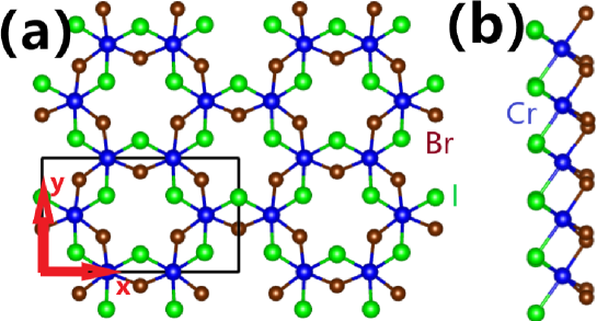
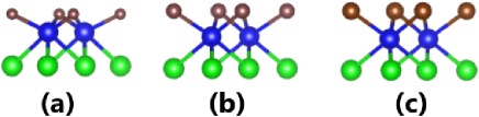
The structure of Janus monolayer is similar to monolayer monolayer, which contains three atomic sublayers with Cr layer sandwiched between Br and I layers. It is well known that Janus transition metal dichalchogenides (TMD) Monolayer MoSSe has been synthesized by replacing the top S atomic layer in with Se atomsp1 . Using the same idea, the Janus monolayer can be constructed by replacing one of two I layers with Br atoms in monolayer . The schematic crystal structures of Janus monolayer are shown in Figure 1. The monolayer has centrosymmetry with point-group symmetry (No.162), but monolayer loses centrosymmetry and horizontal mirror symmetry with point-group symmetry (No.157), which will induce both in-plane and out-of-plane piezoelectricity.
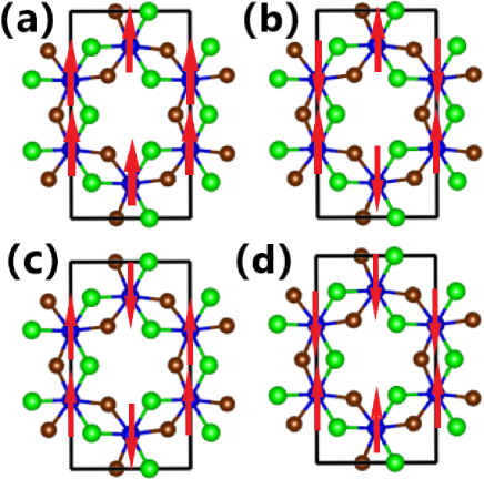
Four different magnetic configurations (Figure 2) are considered to evaluate the magnetic ground state of monolayer , which are used to investigate the ground state of monolayer (X=F, Cl, Br and I)m7-8 . The energy of AF-Nel, AF-zigzag, AF-stripy state and non-magnetic (NM) state with respect to FM state are 56.1 meV, 56.4 meV, 35.2 meV and 6.802 eV with rectangle supercell. Our calculated results show that the FM order is the most stable magnetic state. This means that ferromagnetism in monolayer is retained by elements substitution to construct Janus structure. The optimized lattice constants with FM state is 6.744 , which falls between those of the (6.433 ) and (7.008 ) monolayersm7-8 . For monolayer , the difference in atomic sizes and electronegativities of Br and I atoms leads to inequivalent Cr-Br and Cr-I bond lengths (Br-Cr-Br and I-Cr-I bond angles), and they are 2.542 and 2.719 (92.036 and 89.432), which can induce a built-in electric field.
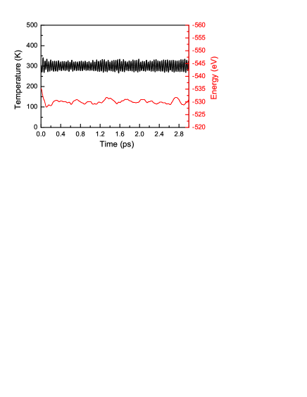
The ab initio molecular dynamics (AIMD) simulations using NVT ensemble are performed to assess the thermal stability of the monolayer at room temperature. Figure 3 shows the temperature and total energy fluctuations of monolayer as a function of the simulation time. Calculated results show no obvious structural disruption with the temperature and total energy fluctuates being small at the end of the MD simulation at 300 K, which confirms the thermodynamical stability of the monolayer at room temperature.
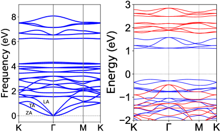
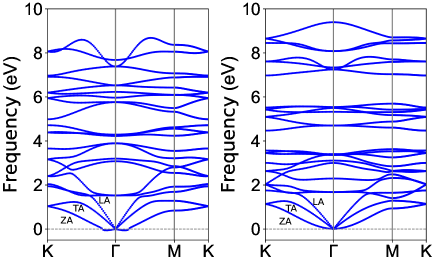
The dynamical stability of the monolayer is analyzed by the phonon spectra, which is plotted in Figure 4. There are twenty-one optical and three acoustical phonon branches with a total of twenty-four branches due to eight atoms per cell. The longitudinal acoustic (LA) and transverse acoustic (TA) modes mean in-plane vibrations, while the ZA branch represents the out-of-plane vibrations. It is clearly seen that the ZA branch is quadratic near the zone center, as typical characteristics of 2D materialsr1 ; r2 . All phonon frequencies are positive, confirming the dynamical stability of monolayer, which means that it can exist as a free-standing 2D crystal.
It is important to check the mechanical stability of monolayer for practical application. Therefore, we calculate elastic constants using the SSR method. Using Voigt notation, the elastic tensor with point-group symmetry for 2D materials can be expressed as:
| (1) |
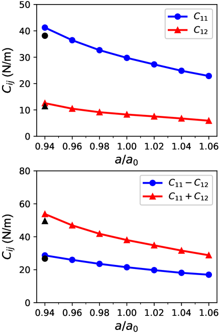
The calculated and are 29.75 and 8.26 , which are between ones of and monolayersm7-8 . The calculated 0 and 0 satisfy the Born criteria of mechanical stabilityela , confirming the mechanical stability of monolayer. We also calculate the Young’s moduli , shear modulus and Poisson’s ratio using the method suggested by Andrew et al, and they are 27.46 , 10.75 and 0.278, respectively. These indicate that monolayer can be easily tuned by strain, which is favorable for novel flexible piezotronics and nanoelectronics.
IV Electronic structure
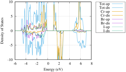
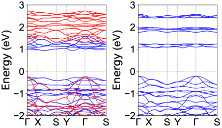
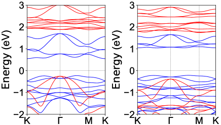
To exhibit piezoelectricity, the monolayer not only should lack inversion symmetry, but also should be a semiconductor. So, we investigate the electronic structures of monolayer with FM ground state, and the energy bands and atomic partial density of states (DOS) are plotted in Figure 4 and Figure 5, respectively. It is found that monolayer is an indirect gap semiconductor with gap value of 1.335 eV. Moreover, the valence and conduction bands near the Fermi level are exclusively contributed by the same spin-up component, showing a typical half-semiconductor character. The difference of the band edge energy between the two spin components for the conduction band minimum (CBM) and the valance band maximum (VBM) are 0.884 eV and 0.233 eV, respectively. According to DOS, the occupied Cr- orbitals are mainly found in the spin-up direction, and the spin-down Cr- states are almost unoccupied. For both spin directions, the conduction band is dominated by Cr- states, which are weakly hybridized with the Br- and I- states. In the spin-down direction, the valence band are almost pure Br- and I- character. For the spin-up direction of the valence band, the states are contributed by the Br- and I- states with a mixture of Cr- states. In fact, many electronic properties of monolayer are similar to ones of monolayerm7-8 .
The magnetic moment of primitive cell is equal to 6 accurately, which is consistent with its semiconducting property. The local magnetic moments of Cr is 2.985 , which suggests that monolayer is robust intrinsic ferromagnetic 2D semiconductor with large magnetic moments. MAE is an important parameter to confirm ferromagnetic behavior of monolayer . The small MAE will result in superparamagnetic rather than ferromagnetic behavior. By using GGA+spin orbital coupling (SOC), it is found that an easy axis is along the c-direction for monolayer , and the corresponding MAE is 356 eV per Cr atom. For and monolayers, the easy axis is also along the c-direction, and the MAE of monolayer is between ones of them (185.5 eV per Cr atom for and 685.5 eV per Cr atom for )m7-8 .
V Piezoelectric properties
The monolayer with point-group symmetry are centrosymmetric, showing no piezoelectricity. The monolayer with point-group symmetry lacks both inversion symmetry and reflectional symmetry across the xy plane, which means that both / and / with defined x and y direction in Figure 1 are nonzero. For 2D materials, only the in-plane strain and stress are taken into accountq7-0 ; q7-1 ; q7-2 ; q7-3 ; q7-4 ; q7-5 ; q7-6 ; q7-7 , and the piezoelectric stress and strain tensors by using Voigt notation can become:
| (2) |
| (3) |
With a applied uniaxial in-plane strain, both in-plane and vertical piezoelectric polarization (/0 and /0) can be produced. However, by imposing biaxial in-plane strain, the out-of-plane one still will remain , while the in-plane piezoelectric response will be suppressed(/=0 and /0). The independent and are can be attained by :
| (4) |
| Name | MAE | EA | |||||||
|---|---|---|---|---|---|---|---|---|---|
| 6.250 | 49.97 | 16.34 | 1.339 | 1.710 | 3.983 | 2.578 | 2151 | ||
| 6.590 | 34.88 | 9.94 | 0.238 | 0.809 | 0.956 | 1.804 | 110 | ||
| 6.744 | 29.75 | 8.26 | 0.119 | 0.432 | 0.557 | 1.138 | 356 |
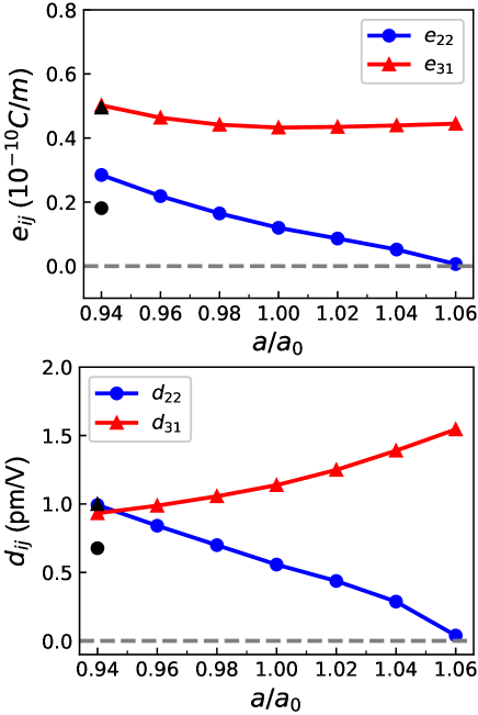
The orthorhombic supercell is used as the computational unit cell (in Figure 1) to calculate the of monolayer. The calculated is 0.119 C/m with ionic part 0.300 C/m and electronic part -0.181 C/m, and for 0.432 C/m with ionic contribution -0.071 C/m and electronic contribution 0.503 C/m. It is found that the electronic and ionic polarizations have opposite signs for both and . The ionic contribution to the in-plane piezoelectricity is larger than the electronic contribution. However, the electronic contributions dominate the out-of-plane piezoelectricity. Based on Equation 4, the and can be attained from previous calculated and . The calculated and are 0.557 pm/V and 1.138 pm/V. A large out-of-plane piezoelectric response is highly desired for 2D materials, which is compatible with the nowadays bottom/top gate technologies. The of monolayer is obviously higher compared with ones of other 2D known materials, including the oxygen functionalized MXenes (0.40-0.78 pm/V)q9 , Janus TMD monolayers (0.03 pm/V)q7-0 , functionalized h-BN (0.13 pm/V)o1 , kalium decorated graphene (0.3 pm/V)o2 , Janus group-III materials (0.46 pm/V)q7-6 , Janus BiTeI/SbTeI monolayer (0.37-0.66 pm/V)o3 and - (0.415 pm/V)o4 . To the best of our knowledge, the is less than one among all pure 2D materials. So, it is very peculiar that the of monolayer is as high as 1.138 pm/V.
VI Strain effects
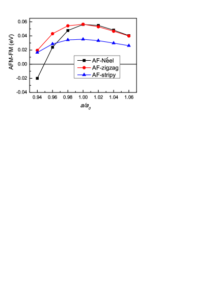
The strain can effectively tune the electronic structures and piezoelectric properties of 2D materialsq7-8 ; q7-9 ; q7-10 . Here, we use to simulate the biaxial strain, where and are the strained and unstrained lattice constants, respectively. To determine the ground state of strained monolayer, four different initial magnetic configurations (Figure 2) are considered. The energy differences of AF-Nel, AF-zigzag and AF-stripy with respect to FM state as a function of strain with rectangle supercell are shown in Figure 6. It is found that a magnetic phase transition can be induced by compressive strain with the critical point being about 0.95, which implies the robustness of the intrinsic ferromagnetism in monolayer. Calculated results show that monolayer prefers FM ground state with being greater than about 0.95 in considered strain range, and the AF-Nel become ground state with being less than about 0.95. Similar phenomenon can also be found in monolayer, and the AF-Nel phase becomes the most stable phase at 0.92 strainm7-8 .
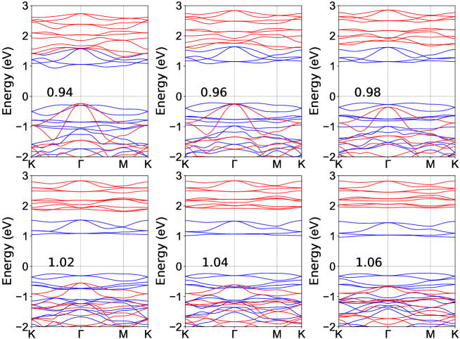
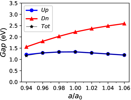
The energy band structures of FM monolayer with strain from 0.94 to 1.06 except 1.00 are plotted in Figure 7, and the majority-spin, minority-spin and total gaps are shown in Figure 8. It is clearly seen that strained monolayer are all indirect gap semiconductors in considered strain range. It is found that the majority-spin and total gaps coincide except 0.94 strain, which means that monolayer holds half-semiconductor character. At 0.94 strain, the VBM is at minority-spin channel from previous majority-spin one. From 1.06 to 0.94 strain, strain makes both conduction and valence bands of minority-spin channel move toward Fermi level, which leads to the reduced minority-spin gap. The majority-spin gap shows a nonmonotonic behavior, which is mainly due to change of CBM. In fact, at 0.94 strain, the AF-Nel becomes ground state, and we plot the energy bands along with FM states in Figure 9 using orthorhombic supercell. The AF-Nel state still is an indirect gap semiconductor with the gap value of 1.282 eV, and the local magnetic moments of Cr is 2.893 .
The strain engineering has been proved to be an very effective way to enhance piezoelectric properties of 2D materials, and then the strain effects on piezoelectric properties of monolayer are performed. The elastic constants including , , - and + of monolayer with FM state as a function of biaxial strain are plotted in Figure 10, along with ones of AF-Nel state at 0.94 strain. It is clearly seen that , , - and + are all decreases with increasing strain from 0.94 to 1.06 strain. It is found that , , - and + with AF-Nel state are lower than ones with FM state at 0.94 strain. So, it is important to consider the magnetic configurations for calculating elastic constants. Calculated results show that the monolayer is mechanically stable in the considered strain range, since the calculated elastic constants satisfy the mechanical stability criteriaela .
The piezoelectric stress coefficients ( and ) along the ionic and electronic contributions and piezoelectric strain coefficients ( and ) of monolayer with FM state as a function of biaxial strain are plotted in Figure 11 and Figure 12, along with ones of AF-Nel state at 0.94 strain. It is found that the compressive strain can enhance the due to improved based on Equation 4, and the improves to 0.993 pm/V at 0.94 strain from unstrained 0.557 pm/V. The tensile strain can decrease the , and the at 1.06 strain reduces to 0.039 pm/V due to very small (0.0066 C/m). For , the opposite strain dependence is observed, and the tensile strain can improve due to reduced +. At 1.06 strain, the of monolayer is 1.545 pm/V, increased by 36% with respect to unstrained one. In considered strain range, the electronic and ionic parts have opposite signs for both and , and they (absolute value) all decreases with strain from 0.94 to 1.06.
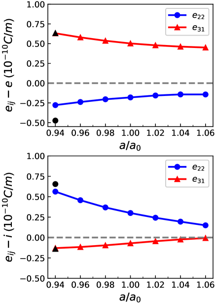
The magnetic configuration may have important effects on piezoelectric coefficients, and a magnetic phase transition may induce the jump of piezoelectric coefficients. We recalculate the and along the ionic and electronic contributions and and of monolayer with AF-Nel state at 0.94 strain. It is found that magnetic configuration has important effect on from 0.285 C/m of FM state to 0.181 C/m of AF-Nel state, and has little influence on (0.502 C/m for FM and 0.495 C/m for AF-Nel). The similar effects on and also can be found, and the () changes from 0.993 pm/V (0.933 pm/V) of FM state to 0.677 pm/V (0.999 pm/V) of AF-Nel state. It is also found that magnetic configuration has important effects on both the electronic and ionic parts of , and has neglectful influences on ones of . So, it is very important to consider magnetic order for piezoelectric coefficients. It is interesting that the PAFM can be induced by compressive strain, which may open up potential opportunities for intriguing physics and novel devices.
VII Discussion and Conclusion
In fact, one of two I layers of monolayer can also be replaced by F or Cl atoms, namely monolayer and . For monolayer, the FM order still is the ground state by comparing energy difference of four different initial magnetic configurations (Figure 2). However, for monolayer , the FM and AF-Nel orders have almost the same energy, and the difference is only 0.48 meV/ formula. So, we focus on the FM state of both monolayer and for a better comparison. For monolayer (), the optimized lattice constants is 6.250 (6.590) , and the calculated and are 49.97 (34.88) and 16.34 (9.94) , which satisfy the Born criteria of mechanical stabilityela . From Figure 13, it is proved that monolayer () is dynamically stable. The side views of crystal structures of (X=F, Cl and Br) are plotted in Figure 14, and it is clearly seen that the distortions of octahedral environment located by Cr atoms become more and more severe with X from Br to Cl to F due to the more difference in atomic sizes and electronegativities of X and I atoms. It is found that an easy axis of monolayer is along the c-direction, and the corresponding MAE is 110 eV per Cr atom. However, for monolayer , an easy axis is along the in-plane direction, and the MAE is up to 2151 eV per Cr atom. Finally, the piezoelectric properties of monolayer and are investigated, and their is up to 2.578 pm/V and 1.804 pm/V, respectively. The related data are summarized in Table 1. In fact, many PFMs can be achieved in 2D (X=F, Cl, Br and I) family by using the same design principle of monolayer , for example Janus monolayer monolayer , , and so on.
In summary, our theoretical calculations demonstrate that the PFM can occur in Janus monolayer with dynamic, mechanical and thermal stabilities, which possesses a sizable MAE. By breaking the inversion and mirror symmetry, both in-plane and out-of-plane piezoelectric polarizations can be induced by a uniaxial in-plane strain. Amazingly, the out-of-plane (1.138 pm/V) is obviously higher compared with ones of many familiar 2D materials. It is proved that strain engineering can effectively tune piezoelectricity of monolayer . The PAFM can also be realized by compressive strain, and () is 0.677 pm/V (0.999 pm/V) at 0.94 strain. Finally, similar to , the PFM can also be achieved in the monolayer and with very large being 2.578 pm/V and 1.804 pm/V. Our works supply an experimental proposal to achieve large out-of-plane piezoelectric response in PFMs, and hope that the work can stimulate further experimental effort on 2D PFM.
Acknowledgements.
This work is supported by Natural Science Basis Research Plan in Shaanxi Province of China (2021JM-456). We are grateful to the Advanced Analysis and Computation Center of China University of Mining and Technology (CUMT) for the award of CPU hours and WIEN2k/VASP software to accomplish this work.References
- (1) W. Wu, L. Wang, Y. Li, F. Zhang, L. Lin, S. Niu, D. Chenet, X. Zhang, Y. Hao, T. F. Heinz, J. Hone and Z. L. Wang, Nature 514, 470 (2014).
- (2) H. Zhu, Y. Wang, J. Xiao, M. Liu, S. Xiong, Z. J. Wong, Z. Ye, Y. Ye, X. Yin and X. Zhang, Nat. Nanotechnol. 10, 151 (2015).
- (3) A. Y. Lu, H. Zhu, J. Xiao, C. P. Chuu, Y. Han, M. H. Chiu, C. C. Cheng, C. W. Yang, K. H. Wei, Y. Yang, Y. Wang, D. Sokaras, D. Nordlund, P. Yang, D. A. Muller, M. Y. Chou, X. Zhang and L. J. Li, Nat. Nanotechnol. 12, 744 (2017).
- (4) M. Dai, Z. Wang, F. Wang, Y. Qiu, J. Zhang, C. Y. Xu, T. Zhai, W. Cao, Y. Fu, D. Jia, Y. Zhou, and P. A. Hu, Nano Lett. 19, 5416 (2019).
- (5) L. Dong, J. Lou and V. B. Shenoy, ACS Nano, 11, 8242 (2017).
- (6) R. X. Fei, We. B. Li, J. Li and L. Yang, Appl. Phys. Lett. 107, 173104 (2015).
- (7) M. N. Blonsky, H. L. Zhuang, A. K. Singh and R. G. Hennig, ACS Nano, 9, 9885 (2015).
- (8) Y. Chen, J. Y. Liu, J. B. Yu, Y. G. Guo and Q. Sun, Phys. Chem. Chem. Phys. 21, 1207 (2019).
- (9) S. D. Guo, Y. T. Zhu, W. Q. Mu and W. C. Ren, EPL 132, 57002 (2020).
- (10) S. D. Guo, Y. T. Zhu, W. Q. Mu, L. Wang and X. Q. Chen, Comp. Mater. Sci. 188, 110223 (2021)
- (11) Y. Guo, S. Zhou, Y. Z. Bai, and J. J. Zhao, Appl. Phys. Lett. 110, 163102 (2017).
- (12) W. B. Li and J. Li, Nano Res. 8, 3796 (2015).
- (13) Dimple, N. Jena, A. Rawat, R. Ahammed, M. K. Mohanta and A. D. Sarkar, J. Mater. Chem. A 6, 24885 (2018).
- (14) S. D. Guo, X. S. Guo, Y. Y. Zhang and K. Luo, J. Alloy. Compd. 822, 153577 (2020).
- (15) N. Jena, Dimple, S. D. Behere and A. D. Sarkar, J. Phys. Chem. C 121, 9181 (2017).
- (16) J. H. Yang, A. P. Wang, S. Z. Zhang, J. Liu, Z. C. Zhong and L. Chen, Phys. Chem. Chem. Phys., 21, 132 (2019).
- (17) S. D. Guo, W. Q. Mu, Y. T. Zhu and X. Q. Chen, Phys. Chem. Chem. Phys. 22, 28359 (2020).
- (18) S. D. Guo, W. Q. Mu, Y. T. Zhu, S. Q. Wang and G. Z. Wang, J. Mater. Chem. C, 2021, DOI: 10.1039/D1TC00414J.
- (19) S. D. Guo, Y. T. Zhu, W. Q. Mu and X. Q. Chen, arXiv:2103.03456 (2021).
- (20) M. T. Ong and E.J. Reed, ACS Nano 6, 1387 (2012).
- (21) A. A. M. Noor, H. J. Kim and Y. H. Shin, Phys. Chem. Chem. Phys. 16, 6575 (2014).
- (22) J. Tan, Y. H. Wang, Z. T. Wang, X. J. He, Y. L. Liu, B. Wanga, M. I. Katsnelson and S. J. Yuan, Nano Energy 65, 104058 (2019).
- (23) L. Dong, H. Kumar, B. Anasori, Y. Gogotsi and V. B. Shenoy, J. Phys. Chem. Lett. 8, 422 (2017).
- (24) Y. Ma, Y. Dai, M. Guo, C. Niu, Y. Zhu and B. Huang, ACS Nano, 6, 1695 (2012).
- (25) C. Gong, L. Li, Z. Li, H. Ji, A. Stern, Y. Xia, T. Cao, W. Bao, C. Wang, Y. Wang, Z. Q. Qiu, R. J. Cava, S. G. Louie, J. Xia and X. Zhang, Nature 546, 265 (2017).
- (26) M. Khazaei, M. Arai, T. Sasaki, C. Y. Chung, N. S. Venkataramanan, M. Estili, Y. Sakka and Y. Kawazoe, Adv. Funct. Mater. 23, 2185 (2013).
- (27) I. Choudhuri, S. Kumar, A. Mahata, K. S. Rawat and B. Pathak, Nanoscale 8, 14117 (2016).
- (28) Y. Guo, H. Deng, X. Sun, X. Li, J. Zhao, J. Wu, W. Chu, S. Zhang, H. Pan, X. Zheng, X. Wu, C. Jin, C. Wu and Y. Xie, Adv. Mater. 29, 1700715 (2017).
- (29) X. M. Wu, Y. L. Feng, S. Li, B. Q. Zhang and G. Y. Gao, J. Phys. Chem. C 124, 16127 (2020).
- (30) B. Huang, G. Clark, E. Navarro-Moratalla, D. R. Klein, R. Cheng, K. L. Seyler, D. Zhong, E. Schmidgall, M. A. McGuire, D. H. Cobden, W. Yao, D. Xiao, P. Jarillo-Herrero and X. Xu, Nature 546, 270 (2017).
- (31) G. Bhattacharyya, I. Choudhuri, P. Bhauriyal, P. Garg and B. Pathak, Nanoscale 10, 22280 (2018).
- (32) W. B. Zhang, Q. Qu, P. Zhu and C. H. Lam, : J. Mater. Chem. C 3, 12457 (2015).
- (33) S. Jiang, J. Shan and K. F. Mak, Nat. Mater. 17, 406 (2018).
- (34) S. Jiang, L. Li, Z. Wang, K. F. Mak and J. Shan, Nat. Nanotechnol. 13, 549 (2018).
- (35) N. Sivadas, S. Okamoto, X. Xu, C. J. Fennie and D. Xiao, 18, 7658 (2018).
- (36) Z. Wang, et al., Nat. Commun. 9, 2516 (2018).
- (37) G. Z. Qin, H. M. Wang, L. C. Zhang, Z. Z. Qin and M. Hu, J. Mater. Chem. C 8, 3520 (2020).
- (38) B. Huang, et al., Nat. Nanotechnol. 13, 544 (2018).
- (39) A. Y. Lu, H. Y. Zhu, J. Xiao et al., Nature Nanotechnology 12, 744 (2017).
- (40) P. Hohenberg and W. Kohn, Phys. Rev. 136, B864 (1964); W. Kohn and L. J. Sham, Phys. Rev. 140, A1133 (1965).
- (41) G. Kresse, J. Non-Cryst. Solids 193, 222 (1995).
- (42) G. Kresse and J. Furthmller, Comput. Mater. Sci. 6, 15 (1996).
- (43) G. Kresse and D. Joubert, Phys. Rev. B 59, 1758 (1999).
- (44) J. P. Perdew, K. Burke and M. Ernzerhof, Phys. Rev. Lett. 77, 3865 (1996).
- (45) X. Wu, D. Vanderbilt and D. R. Hamann, Phys. Rev. B 72, 035105 (2005).
- (46) A. Togo, F. Oba, and I. Tanaka, Phys. Rev. B 78, 134106 (2008).
- (47) E. Mariani and F. V. Oppen, Phys. Rev. Lett. 100, 076801 (2008).
- (48) J. Carrete , W. Li, L. Lindsay, D. A. Broido, L. J. Gallego and N. Mingo, Mater. Res. Lett. 4, 204 (2016).
- (49) R. C. Andrew, R. E. Mapasha, A. M. Ukpong and N. Chetty, Phys. Rev. B 85, 125428 (2012).
- (50) A. A. M. Noor, H. J. Kim and Y. H. Shin, Phys. Chem. Chem. Phys. 16, 6575 (2014).
- (51) M. T. Ong and E. J. Reed, ACS Nano 6, 1387 (2012).
- (52) S. D. Guo, X. S. Guo, Z. Y. Liu and Y. N. Quan, J. Appl. Phys. 127, 064302 (2020).
- (53) L. Hu and X.R. Huang, RSC Adv. 7, 55034 (2017).