Majorana bound states in topological insulators without a vortex
Abstract
We consider a three-dimensional topological insulator (TI) wire with a non-uniform chemical potential induced by gating across the cross-section. This inhomogeneity in chemical potential lifts the degeneracy between two one-dimensional surface state subbands. A magnetic field applied along the wire, due to orbital effects, breaks time-reversal symmetry and lifts the Kramers degeneracy at zero-momentum. If placed in proximity to an -wave superconductor, the system can be brought into a topological phase at relatively weak magnetic fields. Majorana bound states (MBSs), localized at the ends of the TI wire, emerge and are present for an exceptionally large region of parameter space in realistic systems. Unlike in previous proposals, these MBSs occur without the requirement of a vortex in the superconducting pairing potential, which represents a significant simplification for experiments. Our results open a pathway to the realisation of MBSs in present day TI wire devices.
Introduction. The non-Abelian statistics of Majorana bound states (MBSs) makes them a promising basis for fault tolerant quantum computation [1, 2, 3]. Such MBSs were originally predicted to appear at the cores of vortices in spinless topological superconductors [4, 5, 6]. Fu and Kane [7] proposed that a topological superconducting phase with MBSs localised at the centers of superconducting vortices could also be present at the surface of a three-dimensional topological insulator (TI) in proximity to an -wave superconductor [8].
In a related set-up MBSs have been predicted in thin TI wires that are subjected to a magnetic field parallel to the wire and where the phase of the pairing potential of the proximity-induced superconductivity winds around the wire in the form of a vortex [9]. While still in their infancy, TI wire devices have recently seen significant experimental progress [10, 11, 12, 13, 14, 15, 16, 17]. For instance, the growth of very thin (diameter nm) bulk insulating (Bi1-xSbx)2Te3 wires with quantum confined surface states was reported in Ref. 16.
Experimentally the requirement of a vortex in the induced pairing potential essentially necessitates a full superconducting shell, a significant fabrication challenge. For the thinnest wires, where the effects coming from the TI bulk states are weakest, this also requires strong magnetic fields T. When the superconductor is attached to only one side of the wire, such that a vortex is not expected, the superconducting gap in the topological phase was shown to be negligibly small [18, 19, 20], meaning that MBSs have very long localisation lengths and will overlap in realistic finite-length wires. Hence, the prerequisite for a vortex presents a major roadblock to the realisation of MBSs in current TI wire devices.
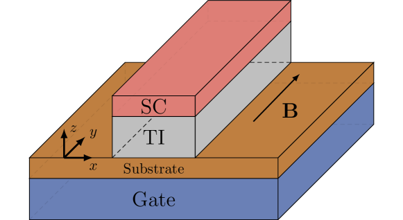
In this work, we propose an alternative protocol for obtaining MBSs in TI wires without the requirement of a superconducting vortex. This is accomplished by a metallic gate placed below the wire and a superconductor attached to the top (as shown in Fig. 1). Such a set-up is very natural since gating will almost always be required to tune the system to the Dirac point [16]. The non-uniform chemical potential induced by a finite gate voltage breaks inversion symmetry, splitting the doubly degenerate one-dimensional (1D) subbands of the quantum confined TI surface states. A magnetic field applied parallel to the wire opens a gap at momentum due to orbital effects and leaves only a pair of (almost) helical modes at finite Fermi momenta. As a result, when, in addition, the superconductivity in the TI wire is induced by proximity to an -wave bulk superconductor, a topological superconducting phase can be achieved. In contrast to a TI wire in which inversion symmetry is not broken by gating, this topological phase, induced without the requirement of a vortex, is characterized by a relatively large superconducting gap in the spectrum. As a consequence the topological phase with well localised zero-energy MBSs occupies an exceptionally large area in parameter space. In realistic wires the range of chemical potential with MBSs spans several meV at relatively weak magnetic field strengths. Our protocol therefore provides a path to realising MBSs in present day TI wire devices.
Subband splitting. We begin with a continuum model for the Dirac surface states of a three-dimensional TI confined to a cylindrical wire. Due to confinement the surface states form 1D subbands labelled by half-integer angular momentum around the wire and with an energy dispersion above the Dirac point given by [21]
| (1) |
and by below the Dirac point. Here, is the perimeter of the wire cross-section, is the momentum along the wire, is the Fermi velocity, and is the magnetic flux induced by the magnetic field applied along the wire in units of the fundamental flux quantum . Inversion symmetry requires that the subbands satisfy and, in the absence of a magnetic field, time reversal symmetry enforces [20, 21]. Therefore, when both symmetries are present, subbands are doubly degenerate for angular momenta at all momenta .
We first consider the influence of the gate in the absence of magnetic fields. Since the gate is placed on only one side of the wire, the resulting electrostatic field gives rise to a non-uniform chemical potential across the wire cross-section [15, 16], where is the average chemical potential and is the angle from the direction normal to the gate (i.e. from the direction in Fig. 1)[21]. This inhomogeneous chemical potential breaks inversion symmetry and therefore lifts the degeneracy of the subbands at finite . Kramers theorem requires that subbands have opposite spins at opposite momenta and at subbands remain degenerate.
More precisely, within this continuum model, one can obtain the subband splitting by expanding the inhomogeneous component of the chemical potential in terms of Fourier cosine harmonics . In general, the inhomogeneous potential causes finite matrix elements between the and subband, where indicates subbands above (+) or below (-) the Dirac point [16, 21]. When the inhomogeneity is small we can use degenerate perturbation theory for the and subbands and label the resulting subband pair by . The th Fourier component of the inhomogeneous potential couples these degenerate subbands and results in a splitting of subbands above the Dirac point
| (2) |
As a result, each subband minimum moves from to a new minimum at , which can be estimated from Eq. (2),
| (3) |
to leading order in the inhomogeneity . The size of the splitting of a given subband pair, , is determined by the change in the subband minimal energy as
| (4) |
Since inhomogeneities are typically of the order of the subband spacing meV [15, 16], the thinnest nm experimental TI wires can achieve splitting energies meV with a corresponding length scale nm. We note that this energy is a very large value when compared to the similar subband splitting caused by Rashba spin-orbit coupling in semiconducting nanowires, which is typically meV in InAs or InSb [22].
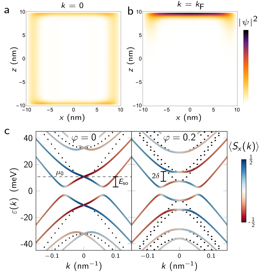
The gate induced splitting of subbands is also confirmed numerically (see Fig. 2) by diagonalising the Bernevig-Hughes-Zhang (BHZ) tight-binding model Hamiltonian in momentum space for a wire with a square cross-section [23, 24, 25, 26]. To connect to realistic experimental systems throughout this manuscript we use parameters consistent with the TI Bi2Se3 [25, 21], choosing wires with a nm nm cross-section and the crystallographic axes and -plane spanning the and directions [16]. As expected from our considerations above, we find that the subband splitting does not strongly depend on the exact choice of the inhomogeneity of the chemical potential and so will be generically be present in any TI wire that has been gated [21]. Although a perturbative result, as seen in Fig. 2, the energy spectrum defined by Eq. (2) is still relevant even for inhomogeneities larger than the subband spacing . In particular, we note that the exact shape of inhomogeneity induced by the gate does not influence the form of the splitting in Eq. (2) other than through the relative sizes of the harmonics . Ultimately the magnitudes of these harmonics will depend on the wire cross section, gate geometry, and electrostatic considerations such as the screening of the superconductor, but in general splitting will be largest close to the Dirac point as the largest will generically occur for small . From Eq. (2) we also see that there is no change in the energy at , which is consistent with the previous observation that such states can be connected by Klein-tunneling through any chemical potential inhomogeneity [15, 16].
Field induced gap. We now consider a magnetic field applied parallel to the wire, see Fig. 1. A magnetic field opens a gap at , leaving an odd number of pairs of counter-propagating modes at the Fermi-level when the chemical potential is tuned close to a subband crossing (dashed line in Fig. 2c). Even in the presence of the gate induced inhomogeneity , due to the Klein-tunnelling effects, the wave function at is uniformly distributed on the wire surface. In contrast, the wave function at is localised close to the top or bottom of the wire, depending on the sign of the corresponding harmonics (see Fig. 2a-b). As a consequence, threading a magnetic flux through the gated TI wire opens a gap at due to orbital effects whereas the states at finite Fermi momenta are largely unaffected by such a flux. The size of the gap is given by [21]. For nm wire this means a gap of meV per T can be opened. In fact, increases linearly with wire thickness, meaning thicker wires open a gap significantly faster. For instance, a thicker nm would open a gap of meV per T. In semiconductor nanowires, which use the Zeeman effect to open an equivalent gap at , this would require a -factor of over 200. The relevant -factor for Bi2Se3 is and so the Zeeman effect in our set-up is negligible compared to orbital effects [25, 21]. Finally, we note that the surface states are spin-polarized in the direction orthogonal to the wire and gate normal (the -axis in Fig. 1) and the spin expectation value in the other two directions is zero, . Therefore if the chemical potential is tuned inside the gap, this setup could be used as a spin-filter with nearly perfect helical modes [27, 28, 29], see Fig. 2c.
From the above considerations, we see that, for our protocol, there is a trade-off between the size of the gap opening at a given field (larger in thicker wires) and the size of the subband splitting (larger in thinner wires). For Bi2Se3 and related TI materials the ideal radius will likely lie in the range nm. In our numerics, we use a nm nm cross-section ( nm) at the lower end of this range since smaller cross-sections are numerically more accessible but this likely exaggerates the magnetic field strengths required for the topological phase. In what follows we will focus on the lowest electron subbands and measure from the subband crossing at . That said, our conclusions remain generally applicable also to higher energy subbands as long as the chemical potential inhomogeneity is strong enough, a fact that may prove useful since the screening of the superconductor will limit the range of average chemical potentials, , accessible in real experiments.
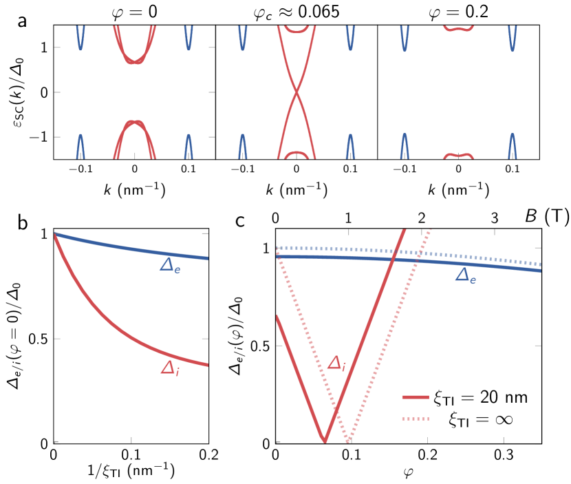
Topological superconductivity. Having established the large splitting of the TI wire subbands as well as the presence of the large magnetic field induced gap , the remaining ingredient required for the appearance of MBSs is a proximity-induced superconductivity. We focus on the setup in which an -wave superconductor is placed on the top of the wire and, therefore, the pairing amplitude is not expected to possess a vortex [20]. A simple model for the spatial dependence of the pairing amplitude in such a set-up is given by [30], where is the superconducting coherence length in the TI. We do not model the reduction of the pairing amplitude by magnetic field but in real systems such an effect will favour thicker wires with a larger gap at a given magnetic field (see above).
Next, we first diagonalise the BHZ tight binding model Hamiltonian in momentum space, where we include the pairing terms of the strength [21] (see Fig. 3). To achieve a large superconducting gap, the sign of the chemical potential harmonic must be such that the state at is localised close to the superconductor. In this case, the exterior superconducting gap, , defined around (shown in blue in Fig. 3a), is essentially unchanged by magnetic field, . On the other hand, the interior gap, , defined around (shown in red in Fig. 3a) is smaller , even in the absence of magnetic fields. This can be explained by the fact that the wave functions at finite Fermi momenta are located close to the superconductor, see Fig. 2b. The amount by which is reduced from depends on the coherence length (see Fig. 3b). As the magnetic field is increased, closes and then reopens, quickly exceeding its zero-field value (see Fig. 3c). The closing and reopening of the gap with magnetic field indicates the onset of a topological superconducting phase. The value at which the superconducting gap closes is found from the following condition [21]:
| (5) |
We note that a finite coherence length, which is responsible for smaller values of without diminishing , allows one to enter the topological phase at weaker magnetic fields.
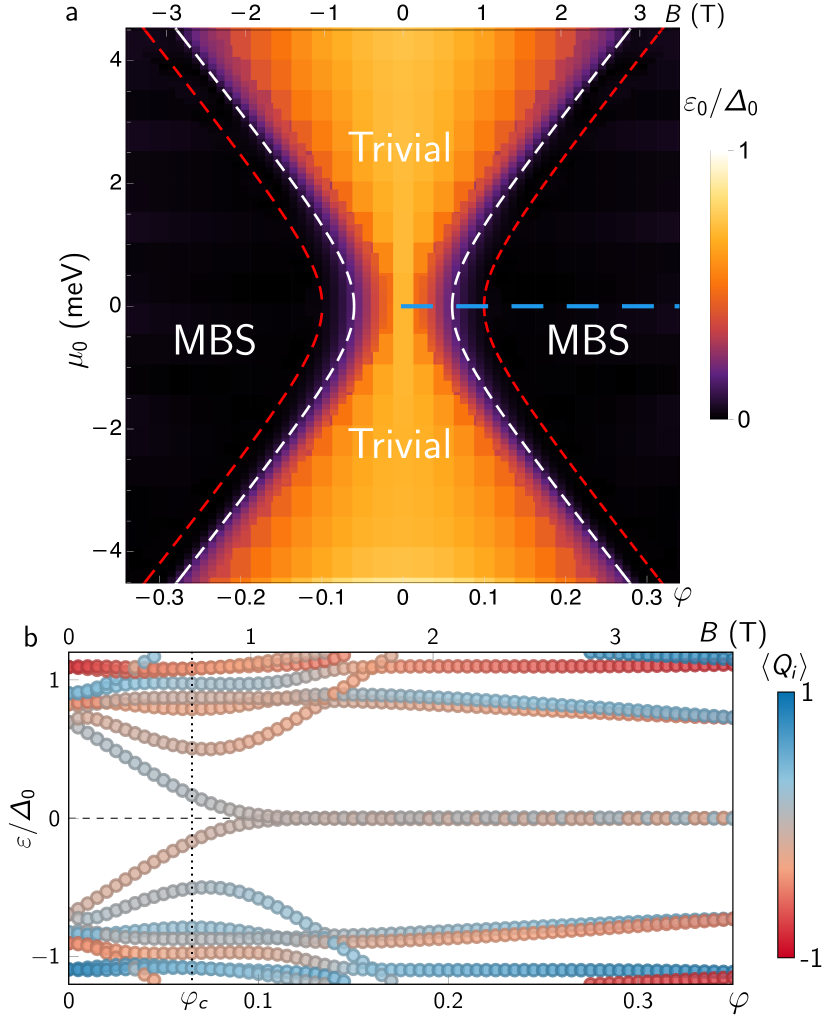
Majorana bound states. To study properties of MBSs in the topological phase we calculate the energy spectrum of a finite wire [21] and obtain the topological phase diagram, see Fig. 4. The white dashed line in Fig. 4a indicates the topological phase transition line obtained in Eq. (5). Inside the topological phase, the MBSs are localized at the ends of the wire and pinned to zero energy, being well-separated from the bulk superconducting states. Close to the phase transition line, the MBSs overlap and split away from zero energy. Thus, generally, the zero-energy MBSs can be observed only if the localization length of MBS , determined by the smallest gap in the spectrum, is smaller than the half of the wire length such that the following criteria is satisfied [31]:
| (6) |
This transition line is indicated by the red dashed line in Fig. 4a. The well-localised zero-energy MBSs persist for a large region of phase space spanning several meV of average chemical potential for fixed finite -fields. As a consequence of this the MBSs are extremely robust against disorder [21]. In stark contrast, without the non-uniformity of chemical potential and with no vortex in the pairing potential, the localisation length condition of Eq. (6) would not be satisfied for any position in phase space and MBSs would overlap and hybridise, moving away from zero energy.
Conclusions. We have shown that it is possible to generate Majorana bound states in topological insulator wires without the requirement of a vortex thanks to a large subband splitting of the 1D surface states arising due to a non-uniform chemical potential across the wire cross-section induced by a gate. In our set-up the topological phase occupies a large region of parameter space and MBSs are very robust against disorder. This may also allow one to systematically eliminate trivial experimental artefacts, a process which can be difficult in other purported MBS systems. Since a vortex is not required in our protocol it opens a path to MBSs in state-of-the-art TI wire devices.
Acknowledgements.
Acknowledgments. We acknowledge useful discussions with Y. Ando, A. Rosch, and M. Rößler. This work was supported by the Georg H. Endress Foundation and the Swiss National Science Foundation and NCCR QSIT. This project received funding from the European Union’s Horizon 2020 research and innovation program (ERC Starting Grant, Grant No 757725).References
- Kitaev [2001] A. Y. Kitaev, Phys. Usp. 44, 131 (2001).
- Ivanov [2001] D. A. Ivanov, Phys. Rev. Lett. 86, 268 (2001).
- Kitaev [2003] A. Y. Kitaev, Ann Phys 303, 2 (2003).
- Volovik [1988] G. Volovik, Sov. Phy.-JETP 67, 1804 (1988).
- Read and Green [2000] N. Read and D. Green, Phys. Rev. B 61, 10267 (2000).
- Alicea [2012] J. Alicea, Rep. Prog. Phys. 75, 076501 (2012).
- Fu and Kane [2008] L. Fu and C. L. Kane, Phys. Rev. Lett. 100, 096407 (2008).
- Hasan and Kane [2010] M. Z. Hasan and C. L. Kane, Rev. Mod. Phys. 82, 3045 (2010).
- Cook and Franz [2011] A. Cook and M. Franz, Phys. Rev. B 84, 201105(R) (2011).
- Hong et al. [2012] S. S. Hong, J. J. Cha, D. Kong, and Y. Cui, Nat. Commun. 3, 1 (2012).
- Hamdou et al. [2013] B. Hamdou, J. Gooth, A. Dorn, E. Pippel, and K. Nielsch, App. Phys. Lett. 103, 193107 (2013).
- Cho et al. [2015] S. Cho, B. Dellabetta, R. Zhong, J. Schneeloch, T. Liu, G. Gu, M. J. Gilbert, and N. Mason, Nat. Commun. 6, 1 (2015).
- Arango et al. [2016] Y. C. Arango, L. Huang, C. Chen, J. Avila, M. C. Asensio, D. Grützmacher, H. Lüth, J. G. Lu, and T. Schäpers, Sci. Rep. 6, 1 (2016).
- Jauregui et al. [2016] L. A. Jauregui, M. T. Pettes, L. P. Rokhinson, L. Shi, and Y. P. Chen, Nat. Nano. 11, 345 (2016).
- Ziegler et al. [2018] J. Ziegler, R. Kozlovsky, C. Gorini, M.-H. Liu, S. Weishäupl, H. Maier, R. Fischer, D. A. Kozlov, Z. D. Kvon, N. Mikhailov, S. A. Dvoretsky, K. Richter, and D. Weiss, Phys. Rev. B 97, 035157 (2018).
- Münning et al. [2021] F. Münning, O. Breunig, H. F. Legg, S. Roitsch, D. Fan, M. Rößler, A. Rosch, and Y. Ando, Nat. Commun. 12, 1038 (2021).
- Breunig and Ando [2021] O. Breunig and Y. Ando, arXiv preprint arXiv:2101.12538 (2021).
- Cook et al. [2012] A. Cook, M. Vazifeh, and M. Franz, Phys. Rev. B 86, 155431 (2012).
- de Juan et al. [2014] F. de Juan, R. Ilan, and J. H. Bardarson, Phys. Rev. Lett. 113, 107003 (2014).
- de Juan et al. [2019] F. de Juan, J. H. Bardarson, and R. Ilan, SciPost Phys. 6, 60 (2019).
- [21] Supplementary material .
- Prada et al. [2020] E. Prada, P. San-Jose, M. W. de Moor, A. Geresdi, E. J. Lee, J. Klinovaja, D. Loss, J. Nygård, R. Aguado, and L. P. Kouwenhoven, Nat. Rev. Phys. 2, 575 (2020).
- Bernevig et al. [2006] B. A. Bernevig, T. L. Hughes, and S.-C. Zhang, Science 314, 1757 (2006).
- Zhang et al. [2009] H. Zhang, C.-X. Liu, X.-L. Qi, X. Dai, Z. Fang, and S.-C. Zhang, Nat. Phys. physics 5, 438 (2009).
- Liu et al. [2010] C.-X. Liu, X.-L. Qi, H. Zhang, X. Dai, Z. Fang, and S.-C. Zhang, Phys. Rev. B 82, 045122 (2010).
- Schulz et al. [2020] F. Schulz, K. Plekhanov, D. Loss, and J. Klinovaja, Phys. Rev. Research 2, 033215 (2020).
- Klinovaja et al. [2011] J. Klinovaja, M. J. Schmidt, B. Braunecker, and D. Loss, Phys. Rev. Lett. 106, 156809 (2011).
- Braunecker et al. [2010] B. Braunecker, G. I. Japaridze, J. Klinovaja, and D. Loss, Phys. Rev. B 82, 045127 (2010).
- Středa and Šeba [2003] P. Středa and P. Šeba, Phys. Rev. Lett. 90, 256601 (2003).
- Flötotto et al. [2018] D. Flötotto, Y. Ota, Y. Bai, C. Zhang, K. Okazaki, A. Tsuzuki, T. Hashimoto, J. N. Eckstein, S. Shin, and T.-C. Chiang, Science Advances 4, eaar7214 (2018).
- Rainis et al. [2013] D. Rainis, L. Trifunovic, J. Klinovaja, and D. Loss, Phys. Rev. B 87, 024515 (2013).