Evidence for a competition between the superconducting spin-valve effect and quasiparticle spin-decay in superconducting spin-valves
Abstract
The difference in the density of states for up- and down-spin electrons in a ferromagnet (F) results in spin-dependent scattering of electrons at a ferromagnet / nonmagnetic (F/N) interface. In a F/N/F spin-valve, this causes a current-independent difference in resistance () between antiparallel (AP) and parallel (P) magnetization states. Giant magnetoresistance (GMR), , is positive due to increased scattering of majority and minority spin-electrons in the AP-state. If N is substituted for a superconductor (S), there exists a competition between GMR and the superconducting spin-valve effect: in the AP-state the net magnetic exchange field acting on S is lowered and the superconductivity is reinforced meaning decreases. For current-perpendicular-to-plane (CPP) spin-valves, existing experimental studies show that GMR dominates () over the superconducting spin valve effect () [J. Y. Gu et al., Phys. Rev. B 66, 140507(R) (2002)]. Here, however, we report a crossover from GMR () to the superconducting spin valve effect () in CPP F/S/F spin-valves as the superconductor thickness decreases below a critical value.
I Introduction
The field of spintronics [1] emerged following the discovery of spin-dependent scattering of electrons at ferromagnetic/nonmagnetic (F/N) interfaces [2] and giant magnetoresistance (GMR) in F/N/F structures [3]. In a F/N/F spin-valve, GMR is the difference in electrical resistance () between antiparallel (AP) and parallel (P) magnetisation states of the F layers and is current-bias independent. In the AP-state, both the majority and minority spin-electrons are strongly scattered and with the magnitude of dependent on the spin-polarization of the F layers, interfacial spin-flip, and the spin decay length in N [4, 5].
In superconducting F/S/F spin-valves [6, 7, 8], the superconducting critical temperature () depends on the magnetic moment orientation of the F layers due to the superconducting spin valve effect: in the P-state, the magnetic exchange fields suppress (P) relative to (AP) in which the magnetic exchange fields partially cancel meaning . This effect allows the superconducting spin-valve to act as a valve for superconducting current flow, demonstrating infinite magnetoresistance, via switching the magnetic state of a device with suitably large held at constant temperature. This current-bias independent behaviour is observed in current-in-plane (CIP) F/S/F spin-valves with reaching tens of mK for transition metal Fs [9, 10, 11, 12, 13, 14, 15, 16, 17, 18] and several hundred mK for rare-earth ferromagnetic metals and insulators [19, 20, 21]. These experimental values of are orders of magnitude smaller than values predicted by theory [6, 7, 8], as it has proven experimentally challenging to reach the theoretically indicated optimum parameter space. Negative values have also been reported [14, 22, 23, 24, 25, 26, 27, 28, 29, 30], attributed either to quasiparticle (QP) spin-accumulation [23, 26, 28] suppressing in the AP-state [31, 32], or flux penetration in S from out-of-plane domain walls in the F layers [14, 24, 27, 30].
Current-perpendicular-to-plane (CPP) devices have larger values of GMR than CIP devices [33, 34, 35, 36], but are less investigated due to the extra complications of fabrication compared to CIP spin-valves, and so investigation into CPP devices with superconducting spin-valves has been limited. One reported CPP device [37] was a F/S/F spin-valve, which showed GMR behaviour () due to quasiparticle transport (“QP GMR”) with a reduced spin decay length relative to the normal state for superconducting Nb layer thicknesses exceeding 30 nm. We note that the superconducting spin-valve effect () was not observed and that superconducting devices with thicknesses below 30 nm were not reported in [37].
In this article, we systematically investigate superconducting CPP F/S/F spin-valves with Py(15)/Cu(10)/Nb()/Cu(10)/Py(15)/FeMn(10) layers (numbers in nm units) sandwiched between 200-nm-thick Cu electrodes (Fig. 1, inset top left). As expected, with decreasing Nb thickness () QP GMR increases; however, below a critical thickness of superconducting Nb ( nm) a sign change in is observed, consistent with the appearance of the superconducting spin valve effect in these CPP devices, which dominates the QP GMR behaviour at these thicknesses. We show a systematic crossover between these competing behaviours, dependent on .
II Experimental
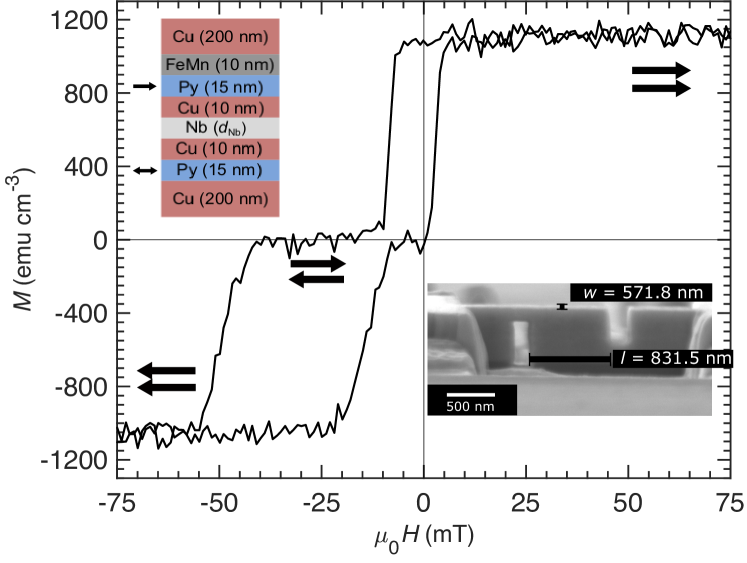
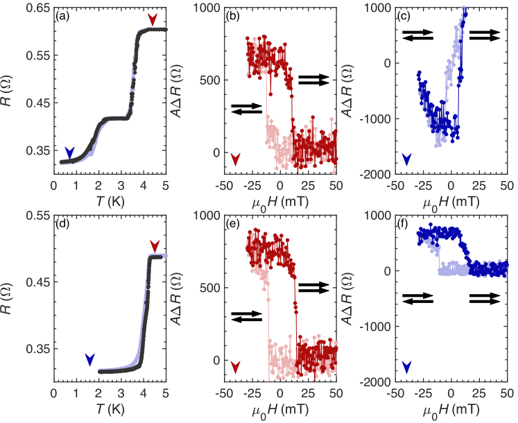
The spin-valves are prepared by dc magnetron sputtering in an ultra-high vacuum chamber with a base pressure better than mbar. Films are deposited onto single crystal silicon with a 250-nm-thick surface oxide, with an in-plane magnetic field (100 mT) applied during growth to set in-plane uniaxial anisotropy. An antiferromagnetic layer of FeMn exchange biases the top layer of Py (Ni80Fe20), ensuring a stable AP-state (Fig. 1). The Cu between the Nb and Py improves interface quality by limiting magnetic dead layers [38, 39, 40], and also increases the magnitude of magnetoresistance [37]. The spin-valves are patterned into nanopillars using optical lithography and Ga-ion focused ion-beam (FIB) etching (described elsewhere [41]). The lengths and widths of the nanopillars vary between 400-1500 nm and 300-1000 nm, respectively. Dimension and resistance values for each device are reported in Table S1 [42]. Resistance of the CPP spin-valves vs. temperature [] or in-plane magnetic field [] is measured using a ‘quasi’ four-point current-bias setup in a pulse-tube measurement system, which removes contact resistance. As Cu contact layers are used, the section under measurement is not exclusively the nanopillar device, but includes part of the patterned structure from which the nanopillar was milled, which is m wide and m long. This section of heterostructure, referred to as the ‘contact leads’, contributes to the measured resistance and so we refer to the measurement as ‘quasi’ four-point. Finally, in CPP measurements, since the cross-sectional areas () of the CPP spin-valves vary, is normalized by multiplying by (i.e. ) [5]. Measurements were made on devices in both the normal state (above the superconducting transition of the nanopillar device and contact leads, but below K) and in the superconducting state, although many devices had such a suppressed transition temperature that they could not be measured in the S state. One important impact of the contact lead resistance is that measurements can appear to contain two distinct superconducting transitions [Fig. 2(a,d)]. The higher temperature transition (‘contact transition’) corresponds to the Nb in the contact leads, whereas the lower temperature transition (‘device transition’) corresponds to the nanopillar device. We define the onset temperature of the latter as , and as the temperature at 50% of the resistance change below (Supplementary Material Section S-IIB [42]).
III Results
and measurements of two devices are shown in Fig. 2. Whilst the normal state loops [Fig. 2(b,e)] indicate GMR behaviour as expected, the superconducting state loops [Fig. 2(c,f)] reveal that two distinct behaviours appear in our devices, which is supported by the device transitions in Fig. 2(a,d); for the device with higher nm, and , consistent with the results in [37], suggesting GMR moderated by quasiparticles (QP GMR). For the device with lower nm is negative [Fig. 2(c)], and . These results are those expected for superconducting spin-valve effect behaviour observed in CIP devices. The resistance increase with increasing field visible in Fig. 2(c) occurs for all superconducting spin-valve effect devices, which all have low values (being mid-transition at measurement temperatures), and therefore exhibit visible resistance increases within an applied magnetic field.
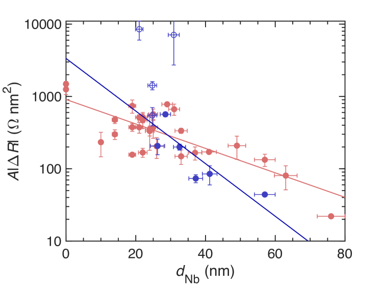
In Fig. 3 we show the absolute value versus , with data points and y-error representing the mean of multiple devices from a single substrate and their standard deviation respectively. Red data are from devices in their normal state (measured at K) and blue data are from devices in the superconducting state at . Open circle data are devices demonstrating the superconducting spin valve effect. By fitting a simple decaying exponential, [43], a reasonable approximation where the thickness of the ferromagnet (15 nm) is much greater than the spin-flip length in the ferromagnet (5.5 nm, [44]), we estimate spin-diffusion lengths from the GMR data in both the normal and superconducting states: nm, and nm. The decay length for QP GMR (in the superconducting state) is shorter than the normal state decay length, as found previously [37].
III.1 Crossover
We now detail the main results of this article. To the best of our knowledge, the superconducting spin-valve effect has not been previously observed in CPP superconducting spin valves, and so we investigate the factors that determine the appearance of this effect.
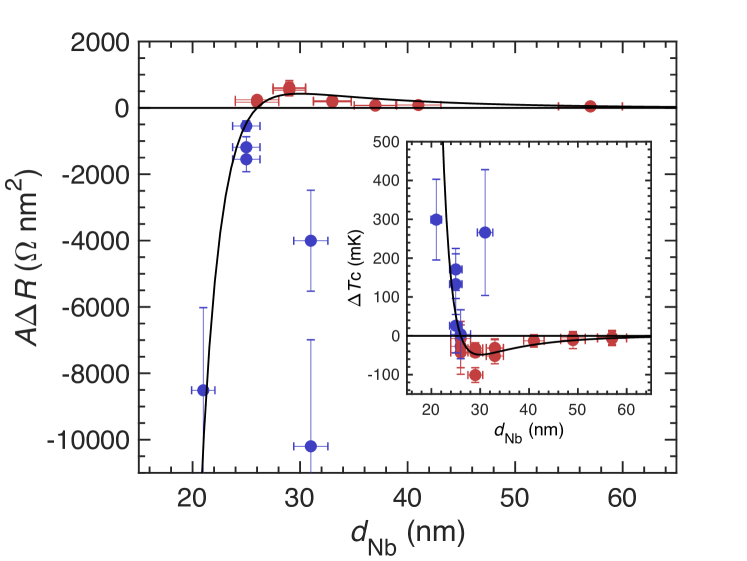
In Fig. 4 we plot at versus , which shows a systematic dependence of on , with a crossover from positive to negative occurring at nm. The inset shows the equivalent trend of versus . For nm, the superconducting spin valve effect reaches a positive up to 299 mK [Fig. S1(a) [42]], which is unprecedented in transition metal F/S/F spin-valves where values are usually of the order tens of mK [9, 10, 11, 12, 13, 14, 15, 16, 17, 18, 22, 23, 24, 25, 26, 27, 28, 29, 30]. However, we note that these large values of are linked to inflation of ; devices showing the superconducting spin-valve effect have suppressed and broadened device transitions [transition width K in Fig. 2(a)], meaning even these large values will not allow infinite magnetoresistance (complete switching between superconducting or normal states at a constant temperature). By considering the impact of superconductivity rather than just , using as the independent parameter, the outlier points at nm were shown to agree far better with the overall trend in the data [Fig. S2(a) [42]]. This led to consideration of the value , where is the dirty limit coherence length in the superconductor, calculated using
where m2s-1 is the electron diffusivity, calculated from a coherence length measurement of an isolated 30 nm Nb film, and is Boltzmann’s constant. Using this normalised , we account for both thickness and processing effects which may affect the superconductivity in the devices. Figure 5 shows at and (Inset) vs. , which shows that the crossover between the two behaviours occurs at around .
Both Fig. 4 and Fig. 5 show the same overall trend: with decreasing , QP GMR (red) increases as expected, but then peaks and decreases rapidly, devices crossing over into superconducting spin-valve effect dominated behaviour, which rapidly increases in magnitude with decreasing . The ‘peak then fall’ shape of the trend indicates that rather than being a sudden switch from QP GMR to superconducting spin-valve effect behaviour, these are two separate effects which compete within the devices.
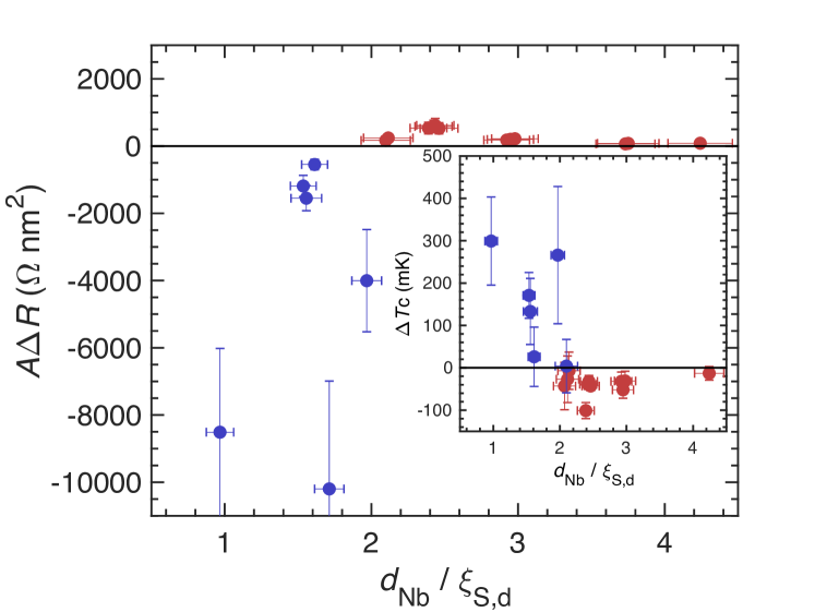
The crossover between positive and negative values of is clear and the magnitude is significant, ruling out minor background effects. Scatter of the data does not account for the crossover behaviour, as indicated by a plot of at normalised by in the normal state [Fig. S2(b) [42]].
IV Discussion
The ‘double’ transition visible within these devices highlights the contribution of the ‘contact leads’ to the measured resistance in these devices. It also highlights that the lower transition - the device transition - tends to be more suppressed in devices demonstrating the superconducting spin-valve effect compared to those demonstrating QP GMR [compare Fig. 2(a) and (d), which feature device transitions around 2 K apart, whereas the ‘contact’ transitions differ by less than 1 K]. This observation suggests not only , but also the strength of superconducting order within the devices affect the appearance of the superconducting spin-valve effect.
Below their superconducting transition, the contact leads are superconducting and do not contribute to the measured response, as shown in the inset to Fig. 6(a), which was measured on the contact leads only. The exception to this is the substrate with thinnest nm: even at the lowest temperatures, the contact leads demonstrate an response which also shows the superconducting spin valve effect [Fig. 6(a)], which may contribute to the large magnitude of the measured effect for that device.
We have considered alternative explanations for the negative in our devices [Fig 2(e)] including anisotropic magnetoresistance [45]. However, this is ruled out since anisotropic magnetoresistance is not observed in these superconducting spin-valve effect devices above [Fig. 2(b)]. Additionally, the zero field measurements show distinct differences between P- and AP-states and anisotropic magnetoresistance would not lead to such differences in the absence of an applied magnetic field [3]. Negative magnetoresistance could also result from crossed Andreev reflection (CAR) [46, 47, 48, 49, 50] of electrons across the superconducting layer, when the layer is less than one superconducting coherence length thick. CAR has previously been considered as a source of magnetoresistance in CIP spin valves [51], but is generally considered as a non-local effect. We note that there is one report of CAR measured in a local setup [52], but the origin of magnetoresistance in this case is uncertain.
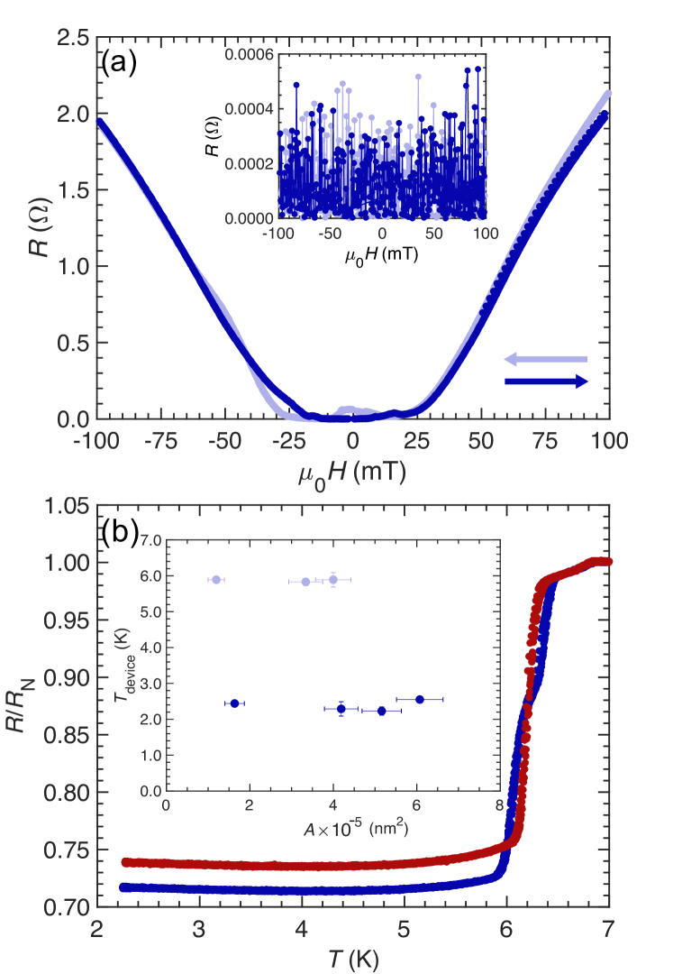
The values for spin decay length calculated in our devices ( nm, and nm) can be compared with other values from the literature. A similar CPP structure has been used previously [37] to measure values of nm and nm. Additionally, a value of nm was extracted from a fit to ferromagnetic resonance data [53]. These literature values are larger than the values measured here; we attribute this difference to increased scattering due to impurities and defects introduced during the nanopatterning process. These defects may also contribute to the separation of device and ‘contact lead’ superconducting transitions. This separation is inconsistent even between devices on the same substrate, as demonstrated in Fig. 6(b), which we cannot currently explain. If FIB milling were accountable for this transition separation, the separation would scale with nanopillar area. However, as shown in the inset to Fig. 6(b), the transition temperature of the device transition, represented by the starting temperature , does not demonstrate any dependence on device area. This uncertainty around the double transition does not affect the main observation of this paper; the appearance of the superconducting spin valve effect in both and measurements and a thickness dependent crossover between them.
The comparison of positive magnetoresistance data above and below supports the suggestion that CPP devices demonstrate QP GMR, as originally demonstrated in [37]. Like in that paper, we also observe a decrease in spin decay length in the superconducting state which is consistent with the additional impact of Andreev reflection causing decay of quasiparticles that cause this magnetoresistance. Unlike [37], we have also measured superconducting devices with smaller than the thickness at which Andreev reflection does not appear to play a role. These devices are those that demonstrate the superconducting spin-valve effect, having negative . The crossover between these two effects appears to occur at around nm, which is close to twice nm, similar to [37], and further supported by Fig. 5, which suggests the crossover occurs where .
IV.1 Phenomenological model
A model in [37] assumes QP GMR in CPP F/S/F spin-valves decays due to Andreev reflection as quasiparticles pass a potential barrier with a temperature-dependent height i.e. , and reduced thickness , where is the thickness of the region near each F/S interface where the superconducting gap and Andreev reflection are suppressed, expected to be equal to the coherence length. This approximation captures the QP GMR results in Fig. 4 beyond nm, but cannot describe our superconducting spin-valve effect data.
We extend these ideas from [37], in a toy model that simply illustrates the two competing effects within our devices, capturing the overall trend as the difference of two exponential decays
where the first term relates to QP GMR (), as in the model from [37] and the second to the superconducting spin valve effect (), with a characteristic decay . We choose an exponential for this decay to reproduce the distinct shape of the data in Fig. 4. In this thinner Nb regime, meaning that the superconducting spin-valve effect enhances [7, 8]; leading to decreased resistance as a greater proportion of the Nb is superconducting. We set nm, the crossover thickness, causing , and set to the value . We find a value for nm as an average and deviation from orthogonal distance regression on the and data, which fits both data sets. This value is very small and does not initially appear to represent a physical length; however, we note previous superconducting spin-valve investigations [11] have seen a dramatic shift from a of 41 mK to “only a few mK” for an increase in of only 1 nm, which could only be modelled by theory using parameters that did not match the estimates of the authors. These short decay lengths may reflect some experimental effects not accounted for by theory based fits. Overall, this toy model illustrates coexistence of the superconducting spin-valve effect and QP GMR, which are competing effects within these devices.
Previous studies showing both positive and negative values of are explained on the basis of stray magnetic fields or vortex flow from a multi-domain state of one or both coupled F layers [14, 29, 54]. In our spin-valves positive is expected due to QP GMR, and a multidomain state with out-of-plane stray magnetic fields would cause positive magnetoresistance within the transition region, which is far from the measurement temperature of our QP GMR data [Fig. 2(b)]. No studies that we are aware of have demonstrated a systematic change of sign of magnetoresistance with , such as the crossover we show here.
V Conclusion
In summary, we have presented evidence for a competition between QP GMR and the superconducting spin valve effect in superconducting CPP spin-valves. Below a Nb thickness of nm, is negative and determined by the superconducting spin valve effect; beyond this critical thickness, is positive with a magnitude that is determined by QP Andeev reflection. This thickness appears to correspond to twice the dirty limit coherence length of the devices. These results are relevant to development of quasiparticle spintronics devices, suggesting devices utilising QP GMR effects should be fabricated with nm, or consider using the superconducting spin valve effect.
Acknowledgements.
This work was funded by the EPSRC through a DTP Studentship (nos. EP/M508007/1 and EP/N509620/1) and Programme Grant (no. EP/N017242/1).References
- Žutic̀ et al. [2004] I. Žutic̀, J. Fabian, and S. Das Sarma, Rev. Mod. Phys. 76, 323 (2004).
- Johnson and Silsbee [1985] M. Johnson and R. H. Silsbee, Phys. Rev. Lett. 55, 1790 (1985).
- Dieny et al. [1991] B. Dieny, V. S. Speriosu, S. S. P. Parkin, B. A. Gurney, D. R. Wilhoit, and D. Mauri, Phys. Rev. B 43, 1297 (1991).
- Valet and Fert [1993] T. Valet and A. Fert, J. Magn. Magn. Mater. 121, 378 (1993).
- Bass [2016] J. Bass, J. Magn. Magn. Mater. 408, 244 (2016).
- Oh et al. [1997] S. Oh, D. Youm, and M. R. Beasley, Appl. Phys. Lett. 71, 2376 (1997).
- Tagirov [1999] L. R. Tagirov, Phys. Rev. Lett. 83, 2058 (1999).
- Buzdin and Vedyayev [1999] A. Buzdin and A. Vedyayev, Europhysics Lett. 48, 686 (1999).
- Gu et al. [2002a] J. Y. Gu, C.-Y. You, J. S. Jiang, J. Pearson, Y. B. Bazaliy, and S. D. Bader, Phys. Rev. Lett. 89, 267001 (2002a).
- Potenza and Marrows [2005] A. Potenza and C. H. Marrows, Phys. Rev. B 71, 180503(R) (2005).
- Moraru et al. [2006a] I. C. Moraru, W. P. Pratt, and N. O. Birge, Phys. Rev. Lett. 96, 037004 (2006a).
- Moraru et al. [2006b] I. C. Moraru, W. P. Pratt, and N. O. Birge, Phys. Rev. B 74, 220507(R) (2006b).
- Miao et al. [2008] G.-X. Miao, A. V. Ramos, and J. S. Moodera, Phys. Rev. Lett. 101, 137001 (2008).
- Zhu et al. [2009] J. Zhu, X. Cheng, C. Boone, and I. N. Krivorotov, Phys. Rev. Lett. 103, 027004 (2009).
- Leksin et al. [2010] P. V. Leksin, N. N. Garif’yanov, I. A. Garifullin, J. Schumann, H. Vinzelberg, V. Kataev, R. Klingeler, O. G. Schmidt, and B. Büchner, Appl. Phys. Lett. 97, 102505 (2010).
- Zhu et al. [2010] J. Zhu, I. N. Krivorotov, K. Halterman, and O. T. Valls, Phys. Rev. Lett. 105, 207002 (2010).
- Leksin et al. [2015] P. V. Leksin, N. N. Garif’yanov, A. A. Kamashev, Y. V. Fominov, J. Schumann, C. Hess, V. Kataev, B. Büchner, and I. a. Garifullin, Phys. Rev. B 91, 214508 (2015).
- Jara et al. [2019] A. A. Jara, E. Moen, O. T. Valls, and I. N. Krivorotov, Phys. Rev. B 100, 184512 (2019).
- Gu et al. [2015] Y. Gu, G. B. Halász, J. W. A. Robinson, and M. G. Blamire, Phys. Rev. Lett. 115, 067201 (2015).
- Li et al. [2013] B. Li, N. Roschewsky, B. A. Assaf, M. Eich, M. Epstein-Martin, D. Heiman, M. Münzenberg, and J. S. Moodera, Phys. Rev. Lett. 110, 097001 (2013).
- Zhu et al. [2016] Y. Zhu, A. Pal, M. G. Blamire, and Z. H. Barber, Nat. Mater. 1, 1 (2016).
- Aarts and Rusanov [2006] J. Aarts and A. Y. Rusanov, Comptes Rendus Phys. 7, 99 (2006).
- Rusanov et al. [2006] A. Y. Rusanov, S. Habraken, and J. Aarts, Phys. Rev. B 73, 060505(R) (2006).
- Steiner and Ziemann [2006] R. Steiner and P. Ziemann, Phys. Rev. B 74, 094504 (2006).
- Singh et al. [2007a] A. Singh, C. Sürgers, and H. v. Löhneysen, Phys. Rev. B 75, 024513 (2007a).
- Singh et al. [2007b] A. Singh, C. Sürgers, R. Hoffmann, H. V. Löhneysen, T. V. Ashworth, N. Pilet, and H. J. Hug, Appl. Phys. Lett. 91, 71 (2007b).
- Stamopoulos et al. [2007] D. Stamopoulos, E. Manios, and M. Pissas, Phys. Rev. B 75, 184504 (2007).
- Leksin et al. [2009] P. V. Leksin, R. I. Salikhov, I. A. Garifullin, H. Vinzelberg, V. Kataev, R. Klingeler, L. R. Tagirov, and B. Büchner, JETP Lett. 90, 59 (2009).
- Hwang et al. [2010] T. J. Hwang, D. H. Kim, and S. Oh, IEEE Trans. Magn. 46, 235 (2010).
- Flokstra et al. [2010] M. Flokstra, J. M. van der Knaap, and J. Aarts, Phys. Rev. B 82, 184523 (2010).
- Takahashi et al. [1999] S. Takahashi, H. Imamura, and S. Maekawa, Phys. Rev. Lett. 82, 3911 (1999).
- Takahashi and Maekawa [2003] S. Takahashi and S. Maekawa, Phys. Rev. B 67, 052409 (2003).
- Pratt et al. [1991] W. P. Pratt, S. F. Lee, J. M. Slaughter, R. Loloee, P. A. Schroeder, and J. Bass, Phys. Rev. Lett. 66, 3060 (1991).
- Lee et al. [1995] S. F. Lee, Q. Yang, P. Holody, R. Loloee, J. H. Hetherington, S. Mahmood, B. Ikegami, K. Vigen, L. L. Henry, P. A. Schroeder, W. P. Pratt, and J. Bass, Phys. Rev. B 52, 15426 (1995).
- Gijs et al. [1995] M. A. Gijs, S. K. Lenczowski, J. B. Giesbers, R. J. van de Veerdonk, M. T. Johnson, and J. B. aan de Stegge, Mater. Sci. Eng. B 31, 85 (1995).
- Eid et al. [2002] K. Eid, D. Portner, J. A. Borchers, R. Loloee, M. Al-Haj Darwish, M. Tsoi, R. D. Slater, K. V. O’Donovan, H. Kurt, W. P. Pratt, and J. Bass, Phys. Rev. B 65, 544241 (2002).
- Gu et al. [2002b] J. Y. Gu, J. A. Caballero, R. D. Slater, R. Loloee, and W. P. Pratt, Phys. Rev. B 66, 140507(R) (2002b).
- Bell et al. [2005] C. Bell, R. Loloee, G. Burnell, and M. G. Blamire, Phys. Rev. B 71, 180501(R) (2005).
- Robinson et al. [2007] J. W. A. Robinson, S. Piano, G. Burnell, C. Bell, and M. G. Blamire, Phys. Rev. B 76, 094522 (2007).
- Tateishi and Bergmann [2010] G. Tateishi and G. Bergmann, Eur. Phys. J. B 73, 155 (2010).
- Bell et al. [2003] C. Bell, G. Burnell, D.-J. Kang, R. H. Hadfield, M. J. Kappers, and M. G. Blamire, Nanotechnology 14, 630 (2003).
- [42] See Supplemental Material at [URL will be inserted by publisher] for (I) data and additional figures, (II) the wires leading to the device and (III) fitting details for above and below fits.
- Park et al. [2000] W. Park, D. V. Baxter, S. Steenwyk, I. Moraru, W. P. Pratt, and J. Bass, Phys. Rev. B 62, 1178 (2000).
- Vila et al. [2000] L. Vila, W. Park, J. A. Caballero, D. Bozec, R. Loloee, W. P. Pratt, and J. Bass, J. Appl. Phys. 87, 8610 (2000).
- Mcguire and Potter [1975] T. R. Mcguire and R. I. Potter, IEEE Trans. Magn. 11, 1018 (1975).
- Deutscher and Feinberg [2000] G. Deutscher and D. Feinberg, Appl. Phys. Lett. 76, 487 (2000).
- Beckmann et al. [2004] D. Beckmann, E. B. Weber, and H. V. Löhneysen, Phys. Rev. Lett. 93, 197003 (2004).
- Beckmann and Löhneysen [2007] D. Beckmann and H. V. Löhneysen, Appl. Phys. A Mater. Sci. Process. 89, 603 (2007).
- Kleine et al. [2009] A. Kleine, A. Baumgartner, J. Trbovic, and C. Schönenberger, Europhys. Lett. 87, 10.1209/0295-5075/87/27011 (2009).
- Webb et al. [2012] J. L. Webb, B. J. Hickey, and G. Burnell, Phys. Rev. B 86, 054525 (2012).
- Giazotto et al. [2006] F. Giazotto, F. Taddei, F. Beltram, and R. Fazio, Phys. Rev. Lett. 97, 087001 (2006).
- Cadden-Zimansky et al. [2007] P. Cadden-Zimansky, Z. Jiang, and V. Chandrasekhar, New J. Phys. 9, 10.1088/1367-2630/9/5/116 (2007).
- Jeon et al. [2018] K.-R. Jeon, C. Ciccarelli, A. J. Ferguson, H. Kurebayashi, L. F. Cohen, X. Montiel, M. Eschrig, J. W. A. Robinson, and M. G. Blamire, Nat. Mater. 17, 499 (2018).
- Hwang and Kim [2012] T. J. Hwang and D. H. Kim, J. Korean Phys. Soc. 61, 1628 (2012).