Concepts of Static vs. Dynamic Current Transfer Length in 2G HTS coated conductors with a Current Flow Diverter Architecture
Abstract
This paper uses both experimental and numerical approaches to revisit the concept of current transfer length (CTL) in second-generation high-temperature superconductor coated conductors with a current flow diverter (CFD) architecture. The CFD architecture has been implemented on eight commercial coated conductors samples from THEVA. In order to measure the 2-D current distribution in the silver stabilizer layer of the samples, we first used a custom-made array of 120 voltage taps to measure the surface potential distribution. Then, the so-called “static” CTL () was extracted using a semi-analytical model that fitted well the experimental data. As defined in this paper, the static CTL on a 2-D domain is a generalization of the definition commonly used in literature. In addition, we used a 3-D finite element model to simulate the normal zone propagation in our CFD samples, in order to quantify their “dynamic” CTL (), a new concept introduced in this paper and defined as the CTL observed during the propagation of a quenched region. The results show that, for a CFD architecture, is always larger than , whereas when the interfacial resistance between the stabilizer and the superconductor layers is the same everywhere. We proved that the cause of these different behaviors is related to the shape of the normal zone, which is curved for the CFD architecture, and rectangular otherwise. Finally, we showed that the NZPV is proportional to , not with , which suggests that the dynamic CTL is the most general definition of the CTL and should always be used when current crowding and non-uniform heat generation occurs around a normal zone.
I Introduction
Second-generation high-temperature superconductor coated conductors (2G HTS CCs) based on REBa2Cu3O7-x (RE = rare earth), sometimes simply called HTS tapes, are expected to be used in many applications where high current density, high field or high mechanical strength is required Trociewitz et al. (2011); Senatore et al. (2014); Maeda and Yanagisawa (2019); Uglietti (2019). However, whatever application is targeted, HTS tapes are prone to develop hot spots, and these hot spots can easily destroy the tape (and even the device that comprises the tape) if no action is taken rapidly. The most common protection action is to cut the current when a hot spot starts to propagate along the tape. A fast propagation of the hot spot, also called normal zone propagation velocity (NZPV), is generally desirable, since it allows detecting rapidly the hot spot using the a voltage rise across the terminals of the tape, often winded as a coil.
The NZPV of a given tape architecture can be measured experimentally, but it can also be deduced from another physical quantity: the current transfer length (CTL) Levin et al. (2009); Lacroix et al. (2014). In Levin et al. (2007), Levin showed that there is a linear relationship between the NZPV and the CTL for classical HTS tape architectures (also called “uniform architecture” in this work), i.e. tapes with a 2-D layered structure and sufficiently high interfacial resistance between the REBCO layer and the silver stabilizer. Provided that the CTL can be easily measured or even determined analytically for such tape architectures, it suggests that the CTL is a good indicator of tape robustness against hot spots: the longer it is, the larger is the NZPV. The CTL is thus an important characteristic of superconducting tapes and wires, and it has been intensively studied over the years for multi-filamentary low temperature superconductors Ekin (1978); Dhalle et al. (1999); Polak et al. (1997), for MgB2 wires Stenvall et al. (2006); Holúbek et al. (2007); Vinod et al. (2010) and of course for 2G HTS CCs Polak et al. (2006); Duckworth et al. (2009); Bagrets et al. (2016).
Despite the existence of many investigations related to uniform superconducting wire architectures Fang et al. (1996); Polak et al. (1997); Duckworth (2001); Usoskin et al. (2002); Levin et al. (2007), in which the definition of the CTL was based on the theory developed for low temperature superconductors Yu et al. (1982); Wilson (1983), the relationship between the NZPV and the CTL has never been established for HTS tape architectures comprising a current flow diverter (CFD) Lacroix and Sirois (2014); Lacroix et al. (2014, 2017), an architecture devised to substantially speed up the NZPV and make quench protection easier.
In this paper, we address explicitly this question using a mixed experimental and numerical simulation methodology, which led us to define two types of CTL, namely a “static CTL”, which is compatible with the classical definition, and a “dynamic CTL”, which is shown to be more general than the classical static definition.
II Experimental approach
II.1 Preparation of samples
The HTS tapes used in this work were 2G HTS CCs fabricated by THEVA THE . The fabrication process was as follows. A 100 m thick Hastelloy (C-276) tape was used as the substrate, after being mechanically grinded and electro-chemically polished to smooth its surface. Then, a 3 m thick film of MgO was deposited by evaporation (e-gun) and textured at the same time. The texturing was obtained with an inclined substrate deposition technique (ISD Bauer et al. (1999a, b); Metzger et al. (2001); Zilbauer et al. (2006)) in an oxygen atmosphere. The film was then capped with an additional 200 nm thick layer of MgO deposited at straight incidence. After that, a 3 m thick layer of GdBaCuO was grown on top of the MgO layer using thermally reactive co-evaporation Kinder et al. (1997). Finally, a 1 m thick silver layer was evaporated all around the tape. All samples used in this work were 5 cm long.
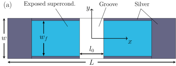
These samples had to be further modified to obtain a “current flow diverter” (or CFD) architecture Lacroix et al. (2014); Lacroix and Sirois (2014). This was done by etching the silver in the center of the tape while keeping the silver intact on its edges, as shown in figure 1(a). When etching the silver, the superconductor becomes exposed to CO2 and water vapor in the air, which creates a very thin amorphous layer (in cyan) that is electrically resistive Russek et al. (1994); Ekin (2006); Lacroix et al. (2014). The width of the etched silver part, noted , was varied for each sample. In total, eight samples with different values varying from 0.0 to 12.0 mm were produced. The silver layer was kept intact (no etching) at the current contacts.
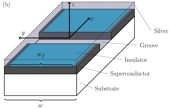
In order to be able to measure the CTL easily, we modified the samples to force the current transfer between the silver and the superconductor layer. The first step was to etch completely the silver on the substrate side and on the edges of the tape. The second step was to create a groove of width in the silver and the superconductor layers across the whole width of the tape, as illustrated in figure 1(a). The silver was etched with a solution of ammonium hydroxide and peroxide diluted in water in a volume ratio of 1:1:4 respectively, then the groove was deepened by etching the superconductor layer with phosphoric acid. The targeted groove width was 10 mm for all samples. Finally, a new silver layer between 1 and 2 m of thickness was sputtered on top of each sample. The final architecture of the samples prior to the electrical characterization is shown in figure 1(b).
After all these fabrication steps, we obtained a set of eight HTS tapes with a CFD architecture and a groove at their middle length. The property of a CFD tape is to exhibit a high electrical resistance at the interface between the superconductor and the silver layers (cyan surface in figure 1), noted cm, and a low electrical resistance at the interface between the superconductor and the silver layers at the edges of the tape, called cm. The values of the interfacial resistances and were measured on two special samples. To measure , a sample with the whole superconductor layer exposed to air was used, whereas to measure , we simply used a virgin THEVA sample. The values found were respectively cm2 and cm2. These measurements were done with the technique described in Fournier-Lupien et al. (2020); Lacroix et al. (2013); Polak et al. (2006).
II.2 CTL measurement setup
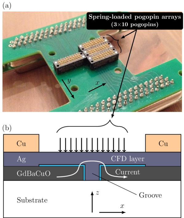
The CTL can be deduced from surface potential measurements performed on a tape, just above the region where current transfers from superconductor to silver or vice-versa. We thus designed and built a homemade sample holder able to map the surface potential in two directions: along the length of the tape and across its width. This 2-D in-plane mapping was required because of the 3-D path followed by the current in the transfer region when considering a CFD architecture (explanations provided later). In this work, four arrays of spring-loaded gold-plated pogo pins 111Hypertac MLPI-30-4-L-SMT with a one millimeter spacing were used, for a total of 120 pogo pins. The four arrays of pogo pins were soldered on a 6-layer PCB, as shown in figure 2(a). For performing a measurement, the pogo pins must be placed above the groove and pressed against the sample.
During the experiments, the sample holder was immersed in liquid nitrogen. The current was injected in the sample using a Keithley 6221 current source via two copper blocks pressed against the sample at both extremities (where the silver has not been etched), see figure 2(b). The injected current was kept low (100 mA) in order to limit the generation of heat.
Using a Keithley 2182A nanovoltmeter, the voltage was measured between a selected pogo pin and a reference pogo pin, located far away from the groove. The voltage of the reference pogo pin was considered to be . The voltage was measured using the delta method Keithley Instruments (2004) in order to cancel any thermoelectric voltage that could be present.
III Experimental results
III.1 Measurement of surface electric potential
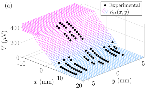
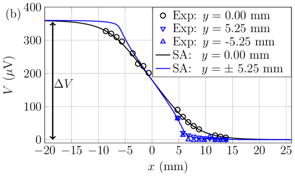
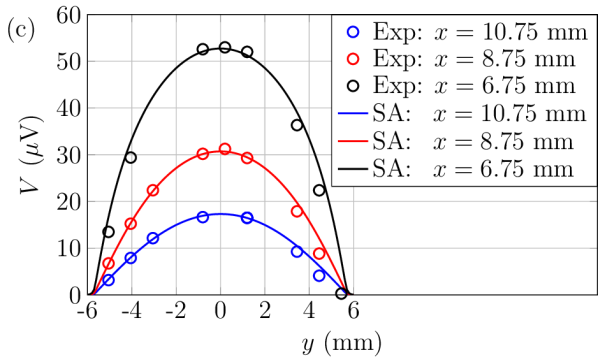
The experimental surface potential distribution was measured on the silver layer for all eight samples with a groove. A typical surface potential measurement with the 120 pogo pins is presented in figure 3(a) (solid black circles). We observe that some data points are missing: this is due to some faulty connections between the pogo pins and the cables connected to the PCB. Figure 3(b) and figure 3(c) show the same data displayed along and (open symbols). In these figures, the groove is centered at .
III.2 Semi-analytical model of the electrical potential
The experimental data were fitted with a semi-analytical model (SA) in order to get a clearer view of the surface potential profile at all (,) points. Knowing the electrical resistivity of silver, one can deduce the local current density everywhere in the silver layer, as well as the total net current flowing in silver, and if necessary, the total net current in the superconductor as well, knowing that no current flows in the Hastelloy substrate due to the electrical insulation properties of the MgO buffer layer. The current in silver is required to obtain the CTL, as described in the next sections.
The detailed development of the SA model can be found in Fournier-Lupien et al. (2020). Only the main points are summarized below. The model assumes that both the silver and the superconductor layers are thin enough to neglect variations of the potential along their thickness , which leads to a description of the problem in terms of the planar Helmholtz equation Levin et al. (2007), i.e.
| (1) |
where is the surface potential of the silver layer, is the potential in the superconducting layer, , where is the conductivity of silver and is the local interfacial resistance, equal to either or . According to figure 1, we can write
| (2) |
The developments in Levin et al. (2007) leads to an exact solution for , which we shall note , expressed as a double infinite summation, i.e.
| (3) |
where are analytical functions (eigenfunctions of a modified Laplace operator) and the coefficient are determined numerically, which explains why the model is qualified as “semi-analytical”.
Once is known, it is possible to find the net current flowing in the silver layer as follows:
| (4) |
where is the thickness of the silver layer, and is the local current density flowing along the length of the tape, given by
| (5) |
Therefore, if the fitting procedure of the SA model with the experimental data is done properly, we have all we need to determine the experimental CTL in our samples.
III.3 Fitting procedure
Seven constant input parameters are required for evaluating Fournier-Lupien et al. (2020). These are , , , , , , . All of them were defined above, except , which corresponds to the total voltage drop resulting from the presence of the groove, see figure 3(b). The first four parameters were measured experimentally. The values used in the SA model were cm2, cm2 and mm. The value of was m for samples 2, 4 and 5, and m for samples 1, 3, 6, 7 and 8.
The last three parameters, i.e. , and , were taken as degrees of freedom for minimizing the least-mean-square error between the SA model and the experimental data points for each sample. The results of this optimization is summarized in table 1. In fact, (width of CFD layer) was also measured experimentally, but since it was hard to be accurate in the fabrication and in the measurement, it was still left free to vary during the optimization, even if the optimizer did not change its value significantly. We thus concluded that the main degrees of freedom for this optimization were and .
Regarding (width of the groove), the different values obtained account for the inaccuracies induced by the two-step etching process of the silver and superconductor layer. As for , it represents a real fitting parameter, since we had no direct measurement of it. An example of the best fit of for sample 5 is presented in figure 3. The fit of the SA model with the experimental data worked well on all samples.
| Measured | Optimized values | |||
| Sample | ||||
| # | (mm) | (mm) | (mm) | (V) |
| 1 | 0.00 | 0.00 | 10.7 | 525 |
| 2 | 9.48 | 9.10 | 11.5 | 360 |
| 3 | 9.50 | 9.50 | 10.5 | 390 |
| 4 | 10.80 | 10.93 | 10.0 | 380 |
| 5 | 11.30 | 11.28 | 12.0 | 360 |
| 6 | 11.50 | 11.40 | 8.6 | 350 |
| 7 | 11.64 | 11.64 | 11.1 | 320 |
| 8 | 12.00 | 12.00 | 10.5 | 1525 |
III.4 Determination of the experimental CTL
Once the electric potential is known everywhere in the silver layer, one can use (4) and (5) to determine , i.e. the total current carried by the silver layer at any point along the length of the tape. Note that corresponds to the current in the middle of the groove, where there is no superconductor. Since silver is the only conducting path at this location, also corresponds to the total current injected in the sample.
Figure 4 shows the current obtained from equation (4), considering the solution shown in figure 3 (data measured on sample 5). From its classical definition, the CTL corresponds to the distance from the edge of the groove where the current in the metallic shunt (here the silver layer) drops by a factor of , i.e. . In other words, is the characteristic length required for the current to transfer from the stabilizer to the superconductor layer. A more detailed discussion about this definition can be found in Fournier-Lupien et al. (2020).
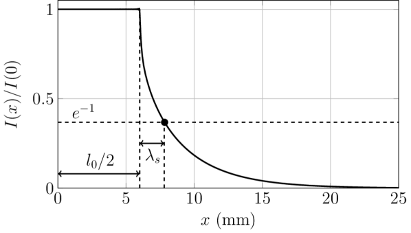
The CTL values determined with this definition for each of the eight samples produced in this work are given in table 2. Since the CTL depends on the thickness of the silver layer, and since the latter was not the same for all samples, we used the fitted values , and for each sample and recalculated their CTL, assuming a fixed thickness of m for the silver layer, which gave a “corrected” value noted in table 2. We use this value later in the paper for comparing our experiments with numerical simulations performed on tapes with 1-m of silver stabilizer. After the correction, we observe that systematically increases as increases, where is the relative width of the CFD layer. This was the expected behavior.
Note that the “” subscript in (or ) stands for “static CTL”, meaning that the current transfer happens at a fixed location over time, here at the edges of the groove. We show later that this CTL can be different from that observed at the extremities of an expanding normal zone (NZ), which we shall call a “dynamic CTL”, noted . Indeed, when a NZ (i.e. hot spot) appears in a HTS tape carrying a current, the latter is forced to transfer in the silver layer to bypass the NZ. If the current generates a sufficient amount of heat, the NZ starts to expand at a specific velocity, called normal zone propagation velocity (NZPV), and the region over which the current transfer occurs follows the front of the NZ.
| Experimental | FE1 model | |||||
|---|---|---|---|---|---|---|
| Sample | NZPV | |||||
| # | no unit | (m) | (mm) | (mm) | (mm) | (cm/s) |
| 1 | 0.00 | 1.1 | 0.07 | 0.06 | 0.08 | 4.8 |
| 2 | 0.76 | 2.0 | 0.76 | 0.71 | 1.70 | 23.8 |
| 3 | 0.79 | 1.1 | 0.87 | 0.87 | 2.00 | 27.1 |
| 4 | 0.91 | 2.0 | 1.62 | 1.52 | 3.30 | 42.8 |
| 5 | 0.94 | 2.0 | 1.83 | 1.72 | 3.69 | 47.8 |
| 6 | 0.95 | 1.1 | 1.80 | 1.78 | 3.81 | 49.1 |
| 7 | 0.97 | 1.1 | 1.97 | 1.95 | 4.11 | 52.7 |
| 8 | 1.00 | 1.1 | 6.36 | 6.09 | 5.45 | 81.2 |
IV CTL during normal zone propagation
We now investigate in details the behavior of the CTL when a quench occurs in HTS tapes. As in the static case, the CTL corresponds to the characteristic length required for the current to transfer from the superconductor to the silver stabilizer surrounding the NZ or vice-versa. However, the dynamic CTL cannot be determined analytically: the highly nonlinear coupling between the electric and the thermal problems makes it too difficult. Therefore, we need to perform numerical simulations for this part of the analysis.
IV.1 Numerical simulations: finite element models
Two finite element (FE) models developed in COMSOL Multiphysics 4.3b were used in this paper. The first one (FE1) simulates the complete dynamic of quench propagation in HTS tapes, whereas the second one (FE2) simulates only the static surface potential on top of the silver layer (no heat equation). The two models are described below.
IV.1.1 FE1 model: simulation of quench in HTS tapes
The FE1 model consists of a 3-D finite element electro-thermal model that simulates the dynamics of quench propagation in HTS tapes, as described in details in Lacroix et al. (2017); Fournier-Lupien et al. (2018a). The model uses the Joule heating module in COMSOL 4.3b, which solves simultaneously the heat equation and the current continuity equation, which are strongly coupled. A NZ is initiated by a local heat pulse at one extremity of the tape. The geometry of the simulated tape is that of a classic CFD architecture Lacroix et al. (2014), exactly as in figure 1, but without the groove. Post-processing on the results allowed extracting , i.e the dynamic CTL.
The characteristic of REBaCuO was modeled using an empirical temperature dependent power law in the flux creep and flux flow regimes Brandt (1996), where V/cm (electric field criterion at 77 K). The transition from the superconducting state to the normal state was modeled by putting the conductivity of the superconducting and the normal state in parallel, such as two resistance in parallel in an electrical circuit. Once again, this is presented in details in Lacroix et al. (2017); Fournier-Lupien et al. (2018a).
In this paper, all the simulations performed with the FE1 model used the following parameters: i) a total current injected in the tape , with A at 77 K, ii) a critical temperature K, iii) an initial temperature of 77 K, iv) a tape width mm, v) interfacial resistances m2 and m2, and vi) a silver layer thickness m. The only parameter that was varied during the simulations was , i.e. the width of the CFD layer.
IV.1.2 FE2 model: simulation of surface potential
The purpose of the FE2 model is to reproduce the experimental results presented in section III and to investigate the effect of the non-superconducting region (groove or NZ) on , the static CTL. The FE2 model is a 3-D finite element model as the FE1 model, but it solves only the current continuity equation, not the heat equation. The temperature in the tape is therefore constant all along the simulation, and the output is the electric potential in the tape. The model uses the Electric currents module in COMSOL 4.3b. For the simulations, the geometry presented in figure 1(b) was implemented, including the groove. The same geometric parameters as in the FE1 model were used with the FE2 model, except for the value of the transport current, which was mA.
IV.2 Simulation of the normal zone propagation
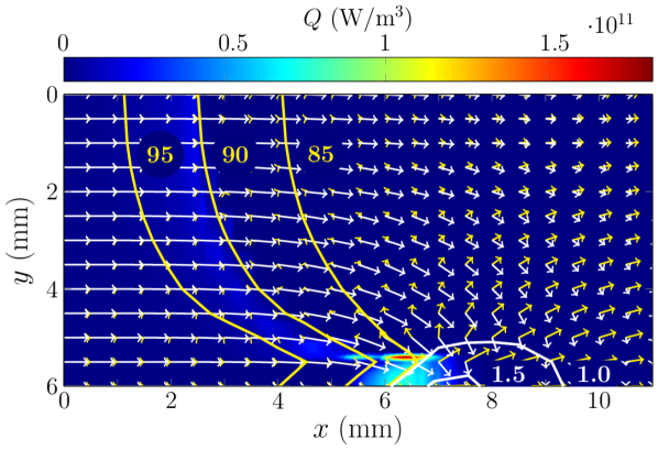
Figure 5 shows a typical simulation output in the plane obtained with the FE1 model. In the simulation, the NZ was generated at and propagated in the direction. The colormap represents the heat generation (W/m3) in the superconductor layer. The arrows represent the local current density in the superconductor (yellow) and in the silver stabilizer (white). The net current flows in the direction. The isolines represent the superconductor temperature in K (yellow) and the magnitude of the current density normalized by the superconductor critical current density at 77 K (white), i.e. .
Since the critical temperature K in the superconductor model, the entire region on the left side of the K isoline corresponds to the NZ. We also observe that the temperature isolines are curved, not straight. These temperature profiles are typical for the CFD architectures and have already been observed experimentally Fournier-Lupien et al. (2018a). The curvature results from a current concentration on the edges of the tape, itself increasing the power density in the superconductor and the local heat generation. Indeed, we clearly see that the current density reaches values larger that in the superconductor, approximately 1 to 2 mm in front of the rightmost point of the NZ. This peculiar concentration, sometimes called “current crowding”, plays a key role in the determination of the CTL.
IV.3 Determination of the CTL from simulations
We used the same definition as in section III.4 to extract the CTL from the finite element simulations, i.e. . Note that we used the notation in this case (dynamic CTL), since the current transfert region moves dynamically over time as the NZ expands. The boundary of the NZ is defined as the K isoline in the middle of the tape, i.e. on the axis in figure 5. Figure 6(a) illustrates how we used this definition to deduce at three different times of the simulation, namely 3 ms, 15 ms and 30 ms. We clearly see that the K point moves to the right as time increases, showing that the NZ expands. The value of is thus simply obtained by calculating the distance between the NZ boundary and the point where the normalized current has decreased to .
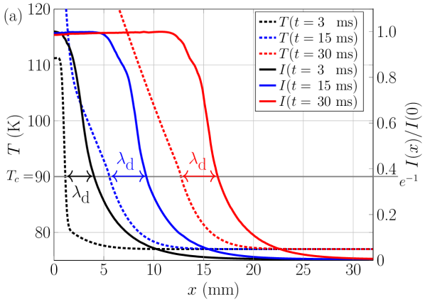
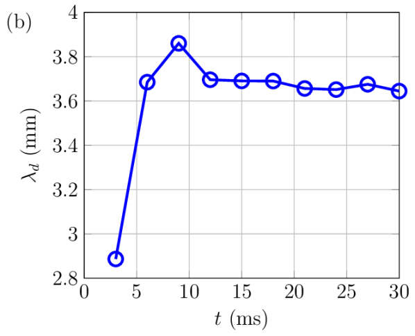
By repeating this process at many time steps, we obtained the evolution of as a function of time, illustrated in 6(b). We observe that it takes about 12 ms before reaches a steady state value. For the purpose of our analysis, we disregard the transient part and consider only the steady-state (constant) value of .
Many such simulations were performed to determine with the FE1 model for the CFD architecture, for values of ranging between 0 and 1, with and having constant values of and .cm2, respectively. The results are presented in figure 7 (solid blue triangles). Numerical values of corresponding to the specific values of our measured samples are also reported in table 2, together with the simulated NZPV values. We clearly see in the figure how increases rapidly with up to , and then remains quite constant. This explains why we usually chose a coverage fraction between 0.8 and 0.9 for the CFD layer.
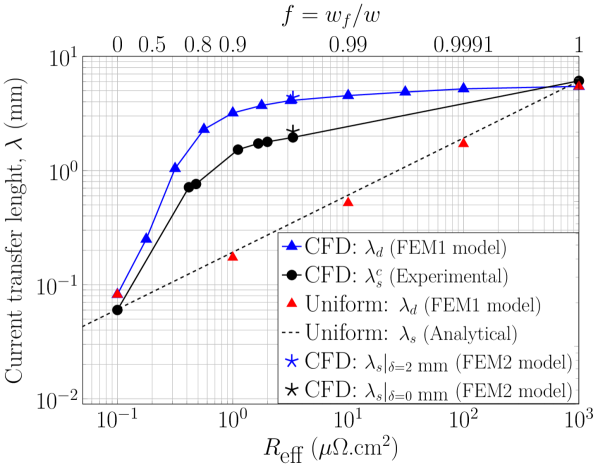
We also used the FE1 model to calculate the values of the uniform architecture (red triangles), which can be seen as a CFD architecture with but with a variable value, here between to cm2. The simplest way to plot the two architectures on the same axis is to define the effective interfacial resistance of the tape as
| (6) |
For the uniform architecture, the decrease of the current in the stabilizer is exponential, i.e. , with . This analytical value of was added in figure 7 (black dotted line) for the sake of validation of the numerical simulations (red triangles). We see that obtained with the analytical solution and obtained numerically with the FE2 model are essentially equivalent, as expected.
Finally, we also added in figure 7 the measured CTL values (the corrected values) reported in table 2 (black circles) to support the discussion presented in next section. Note that these experimental values match perfectly the analytical values of for and , which gives us confidence in our experimental procedure.
IV.4 Discussion about static and dynamic CTL
We observe in figure 7 that the CTL always increases monotonically as increases, or alternatively, as increases for the CFD architecture. We also observe that the CFD architecture leads to larger values of both and with respect to the uniform architecture, except for or , in which the two architectures are equivalent. However, the fundamental difference between these architectures is that for the uniform architecture, whereas for the CFD architecture. We develop the reasons below, after recalling the difference between the two types of CTL.
The static CTL corresponds to the CTL value when no heat generation is present. This is what we measured, for instance, in section II of this paper when we used a very small current in samples where a groove had been voluntarily added to break the continuity of the superconducting path. We can also obtain by numerical simulation if we solve solely the electrical problem and ignore the heat generation, as the FE2 model described above does. Note that the notion of static CTL does not exclude the existence of current crowding around the non-superconducting region.
The dynamic CTL corresponds to the CTL value when we consider thermal effects, and especially the NZ propagation. For observing , it is necessary to apply currents higher than the local , or at least higher than the weakest superconducting region of the tape, to ensure sufficient heating occurs. So far, we have not found a straightforward way to determine experimentally, so we always had to compute it by numerical simulation (FE1 model in this paper).
Based on the above definitions, since and are essentially equal for the uniform architecture, it means that the CTL of the uniform architecture is not affected by the thermal dynamics of the NZ propagation. Conversely, for the CFD architecture, is systematically larger than , thus the CTL is affected by the thermal dynamics of the NZ. We shall see in next section that the condition required for and to be different is to introduce curvature in the shape of the NZ.
IV.5 Shape of the normal zone vs. CTL
It was shown in figure 5 (yellow isolines) that the boundary of the NZ is curved for the CFD architecture. This was in fact known since the original paper on the CFD concept (see figure 4 in Lacroix and Sirois (2014)), but the impact on the CTL had never been properly explained so far. In the same paper, it was also shown that the boundary of the NZ for the uniform architecture is a straight line rather than a curve Lacroix and Sirois (2014).
To analyze the effect of the NZ shape on the CTL, we used the FE2 model (3-D electric potential, no thermal equation) to compute the static CTL on the sample geometry presented in figure 1, for different shapes of the NZ. Note that this model solves the same equations as the SA model does, but with arbitrary shapes of NZ, which the SA model cannot do. The following function was used to model the curved boundary of the NZ:
| (7) |
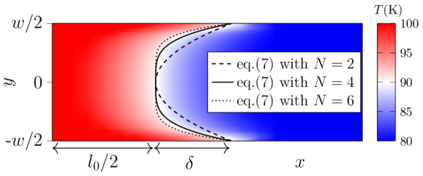
where and are tuning parameters used to produced the curved boundary. If , then , i.e. we have a rectangular NZ (or a groove) whose width is . If , we have a rectangular NZ augmented by an additional curved region, as illustrated in figure 8. Note that this trick allows emulating in a purely geometric manner the curvature of the normal zone that normally arises from the thermal problem.
To find the values of and that best fit our simulation results, we superimposed equation (7) to the temperature map obtained with the FE1 model for a CFD tape with (see figure 8) and found that mm and were good choices. We then ran multiple simulations with the FE2 model for and various values of between 0 mm (rectangular NZ) and 3 mm (NZ with curved boundary). The simulations were run for three different CFD tapes ( values of 0.79, 0.9 and 0.97, respectively).
The static CTL values obtained, which we shall note to emphasize the fact that we voluntarily modified the shape of the NZ boundary, were plotted in figure 9 and show an approximately linear increase with the width of the curved region of the NZ. Remember that in reality, the curvature results from the existence of a non-uniform interfacial resistance between the superconductor and silver layers (because of the CFD layer), which induces 3-D current flow paths and current crowding (geometric effect), which in turn induces heat generation if the current is high enough (thermal effect). All these effects must be present to observe the NZ curvature.
We also added in figure 9 the experimental value (black circle) for sample 7 (), which was expected to fall on the black curve when (the groove then acts as the NZ). The point actually falls below the curve, but this is considered within the experimental error and thus confirms the validity of the simulations.
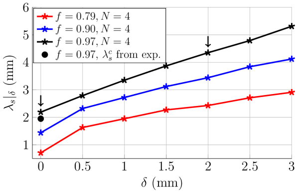
To complete the demonstration of the influence of the shape of the NZ on the CTL, we reported in figure 7 two specific values of the calculated in figure 9 (star markers), namely and , both corresponding to the case and . We clearly see in figure 7 that the point (black star) falls very close to the experimental static CTL curve (solid black circles), and that the point (blue star) falls very close to the dynamic CTL value (solid blue triangles). Since both points were calculated with the FE2 model, providing by definition a static CTL value, it is now clear that the primary factor affecting the CTL is the geometric shape of the NZ.
This raises an interesting point about the definition of the CTL. The classic definition of the CTL is that of , the static CTL, which does not consider thermal effects Ekin (1978); Stenvall et al. (2006). However, we have proved that we can retrieve the dynamic CTL from the definition of by considering the shape of the NZ when calculating the static CTL (noted above). By doing this, we have decoupled the geometric and thermal effects in the determination of the CTL. When considering the uniform tape architecture, this decoupling is pointless since the NZ is rectangular (or nearly rectangular) during a quench propagation, and , which means that the heat propagation is essentially 1-D and has no impact on the CTL. However, with the CFD architecture, the strong current crowding on the edges of the tape (3-D behavior) provides the geometric effect required to trigger inhomogeneous heating (thermal effect), which in turn produces the curved iso-temperature lines of figure 5, thus the curved normal zone boundary. In this case, we have , where is the CTL resulting from the sole geometric effect (rectangular NZ), and is the CTL resulting from the combination of the geometric and thermal effects (NZ with curved boundaries).
Finally, this also explains why in CFD tapes is systematically larger than in uniform tapes for the same values of (see black circles vs red triangles in figure 7). Since no thermal contribution enters in the definition, the difference come exclusively from the geometric effect (current crowding) present in CFD tapes, and not present in uniform tapes. Note that this conclusion applies without the need to invoke any curvature in the shape of the NZ, as shown in figure 7 for tapes with rectangular grooves acting as the NZ.
At this point, if we focus only on the CFD architecture, there remains three important questions to answer, namely: 1) How are and related to each other? 2) How is the NZPV related to and ? 3) Is it worth the extra work of determining ? The next section provides answers to these questions.
V Further considerations about and in CFD tapes
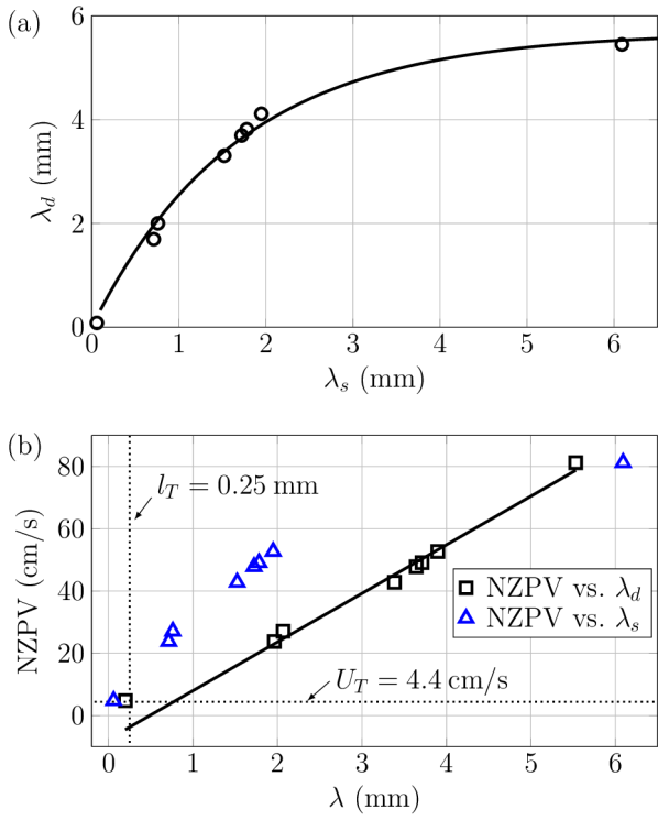
Figure 10(a) shows a plot of (simulated) versus (measured) for the eight CFD samples considered in this paper. The points can be well fitted by an exponential relationship such as , with mm and mm-1. Although this is a simple relationship, it is not clear from this single experiment how the and parameters would vary with the numerous geometric parameters defining a CFD tape architecture, but it would be an interesting avenue to explore.
In figure 10(b), we plotted the calculated NZPV values as a function of the calculated values (all values were taken directly from table 2), for the eight CFD samples investigated. Both quantities were calculated with the FE1 model, but the NZPV could have been measured experimentally. It is striking from this figure that the NZPV is directly proportional to , the dynamic CTL. There is no such nice relationship between the NZPV and the measured values (blue triangles).
When looking more closely at the NZPV vs. plot, we see that only the first point of the curve does not fit well with the linear relationship. This point corresponds to , i.e. a tape without CFD. This does not come as a surprise, since Levin showed in Levin et al. (2009) that the NZPV is proportional to the CTL only when the CTL is larger than the thermal diffusion length . Using Levin’s equations in Levin et al. (2009), we find mm (a constant) for the HTS tapes considered in this work. This implies that the NZPV varies linearly only for , which is consistent with what we see in figure 10(b). For , the NZPV converges towards a constant value noted , equal to 4.4 cm/s in the current case Levin et al. (2009). Therefore, the apparent outlier data point perfectly fit with the theory.
As a final comment, the clear proportionality observed between the NZPV and suggests that the dynamic CTL is more adequate than the static CTL for studying HTS tapes with CFD-like architectures. The dynamic CTL should thus probably be considered as the true general definition of the CTL. Therefore, to answer our last question, it seems that calculating of CFD tapes is worth the effort. In addition, the perfect linear relationship found between the NZPV and might provide an experimental way to relate the measurable static CTL to the “more-difficult-to-measure” dynamic CTL in future work.
VI Conclusion
In this work, we used a mixed experimental and numerical simulation methodology to show for the first time that the current transfer length (CTL) in 2G HTS tapes result from two distinct effects, namely i) a geometric effect, and ii) a thermal effect. The geometric effect is caused by a non-uniform interfacial resistance between the superconductor and the stabilizer layers, and results in non-uniform current transfer pattern (2-D effect) and current crowding. The thermal effect consists in inhomogeneous heat generation during the current transfer, with higher heat generation in the higher current density regions. The thermal effect, if strong enough, generates curvature in the normal zone (NZ) boundaries, which in turn affects the current flow paths. Two conditions are required to observe thermal effects: i) the transport current must be high enough, and ii) the geometric effect (current crowding) must be present.
Based on these observations, we could defined two types of CTL, namely i) the static CTL , which corresponds to a CTL that considers solely the geometric effect (no heat propagation), and ii) the dynamic CTL , which takes into account both the geometric and thermal effects. Note that corresponds to the classical definition of the CTL. For uniform HTS tape architectures, which correspond essentially to nowadays commercial tapes, and are equal, since no significant geometric effect is present. However, for the CFD tape architecture, there is a clear distinction between and , with being systematically larger than . Furthermore, because of the geometric effect present in the CFD architecture, in CFD tapes is systematically larger than in uniform tapes.
As a final observation, we confirmed that the normal zone propagation velocity (NZPV) in HTS tapes is proportional to , not to , which strongly suggests that is a more general definition of the CTL than . Therefore, in order to perform a fair comparison between any type of HTS tape architecture, in particular CFD-like architectures Lacroix and Sirois (2014); Fournier-Lupien et al. (2018b), the dynamic CTL should always be used.
VII Acknowledgement
The authors would like to thank Marc-Antoine Huet for the design and realization of the multiplexer system used with the pogo pin arrays. They also thank Mohammed Amine Drai for the design of the 6-layer PCB on which the arrays were soldered. Finally, J.-H. Fournier-Lupien and F. Sirois gratefully thank Prof. Mathias Noe for hosting them at KIT in 2015-2016, where this work was initiated.
References
- Trociewitz et al. (2011) U. P. Trociewitz, M. Dalban-Canassy, M. Hannion, D. K. Hilton, J. Jaroszynski, P. Noyes, Y. Viouchkov, H. W. Weijers, and D. C. Larbalestier, Applied Physics Letters 99, 202506 (2011).
- Senatore et al. (2014) C. Senatore, M. Alessandrini, A. Lucarelli, R. Tediosi, D. Uglietti, and Y. Iwasa, Superconductor Science and Technology 27, 103001 (2014).
- Maeda and Yanagisawa (2019) H. Maeda and Y. Yanagisawa, Journal of Magnetic Resonance 306, 80 (2019).
- Uglietti (2019) D. Uglietti, Superconductor Science and Technology 32, 053001 (2019).
- Levin et al. (2009) G. Levin, K. Novak, and P. Barnes, Superconductor Science and Technology 23, 014021 (2009).
- Lacroix et al. (2014) C. Lacroix, Y. Lapierre, J. Coulombe, and F. Sirois, Superconductor Science and technology 27, 055013 (2014).
- Levin et al. (2007) G. A. Levin, P. N. Barnes, and J. S. Bulmer, Superconductor Science and Technology 20, 757 (2007).
- Ekin (1978) J. Ekin, Journal of Applied Physics 49, 3406 (1978).
- Dhalle et al. (1999) M. Dhalle, L. Porcar, M. Ivancevic, A. Polcari, Y. Huang, G. Witz, and R. Flukiger, IEEE transactions on applied superconductivity 9, 1093 (1999).
- Polak et al. (1997) M. Polak, W. Zhang, J. Parrell, X. Cai, A. Polyanskii, E. Hellstrom, D. Larbalestier, and M. Majoros, Superconductor Science and Technology 10, 769 (1997).
- Stenvall et al. (2006) A. Stenvall, A. Korpela, J. Lehtonen, and R. Mikkonen, Superconductor Science and Technology 20, 92 (2006).
- Holúbek et al. (2007) T. Holúbek, M. Dhallé, and P. Kováč, Superconductor Science and Technology 20, 123 (2007).
- Vinod et al. (2010) K. Vinod, N. Varghese, S. Rahul, K. Devadas, S. Thomas, P. Gurusamy, S. Kedia, S. Pradhan, and U. Syamaprasad, Superconductor Science and Technology 23, 105002 (2010).
- Polak et al. (2006) M. Polak, P. Barnes, and G. Levin, Superconductor Science and Technology 19, 817 (2006).
- Duckworth et al. (2009) R. C. Duckworth, F. A. List, and Y. Zhang, IEEE transactions on applied superconductivity 19, 3327 (2009).
- Bagrets et al. (2016) N. Bagrets, G. Celentano, A. Augieri, R. Nast, and K.-P. Weiss, IEEE Transactions on Applied Superconductivity 26, 1 (2016).
- Fang et al. (1996) Y. Fang, S. Danyluk, Y. Cha, and M. T. Lanagan, Journal of applied physics 79, 947 (1996).
- Duckworth (2001) R. C. Duckworth, “Contact resistance and normal zone formation in coated yttrium barium copper oxide superconductors,” (2001).
- Usoskin et al. (2002) A. Usoskin, A. Issaev, H. Freyhardt, M. Leghissa, M. Oomen, and H.-W. Neumueller, Physica C: Superconductivity 372, 857 (2002).
- Yu et al. (1982) D. Yu, Y. Eyssa, and P. Zolliker, in Advances in Cryogenic Engineering Materials (Springer, 1982) pp. 701–709.
- Wilson (1983) M. Wilson, Superconducting Magnets (Oxford, 1983).
- Lacroix and Sirois (2014) C. Lacroix and F. Sirois, Superconductor Science and Technology 27, 035003 (2014).
- Lacroix et al. (2017) C. Lacroix, F. Sirois, and J. F. Lupien, Superconductor Science and Technology 30, 064004 (2017).
- (24) “THEVA GmbH website,” https://www.theva.com/, accessed: 2020-09-06.
- Bauer et al. (1999a) M. Bauer, R. Semerad, and H. Kinder, IEEE transactions on applied superconductivity 9, 1502 (1999a).
- Bauer et al. (1999b) M. Bauer, R. Metzger, R. Semerad, P. Berberich, and H. Kinder, MRS Online Proceedings Library Archive 585 (1999b).
- Metzger et al. (2001) R. Metzger, M. Bauer, K. Numssen, R. Semerad, P. Berberich, and H. Kinder, IEEE transactions on applied superconductivity 11, 2826 (2001).
- Zilbauer et al. (2006) T. Zilbauer, P. Berberich, A. Lümkemann, K. Numssen, T. Wassner, and G. Sigl, Superconductor Science and Technology 19, 1118 (2006).
- Kinder et al. (1997) H. Kinder, P. Berberich, W. Prusseit, S. Rieder-Zecha, R. Semerad, and B. Utz, Physica C: Superconductivity 282, 107 (1997).
- Russek et al. (1994) S. E. Russek, S. C. Sanders, A. Roshko, and J. Ekin, Applied physics letters 64, 3649 (1994).
-
Ekin (2006)
J. Ekin, Experimental techniques
for low-temperature
measurements: cryostat design, material properties and superconductor critical-current testing (Oxford university press, 2006). - Fournier-Lupien et al. (2020) J.-H. Fournier-Lupien, P. Del Vecchio, C. Lacroix, and F. Sirois, Superconductor Science and Technology 33, 115014 (2020).
- Lacroix et al. (2013) C. Lacroix, J.-H. Fournier-Lupien, K. McMeekin, and F. Sirois, IEEE transactions on applied superconductivity 23, 4701605 (2013).
- Note (1) Hypertac MLPI-30-4-L-SMT.
- Keithley Instruments (2004) I. Keithley Instruments, Low Level Measurements Handbook, 6th Edition, Precision DC Current, Voltage and Resistance Measurements, Tech. Rep. (2004).
- Fournier-Lupien et al. (2018a) J. Fournier-Lupien, C. Lacroix, S. Hellmann, J. Huh, K. Pfeiffer, and F. Sirois, Superconductor Science and Technology 31, 125019 (2018a).
- Brandt (1996) E. H. Brandt, Physical review B 54, 4246 (1996).
- Fournier-Lupien et al. (2018b) J. Fournier-Lupien, C. Lacroix, S. Hellmann, J. Huh, K. Pfeiffer, and F. Sirois, Superconductor Science and Technology 31, 125019 (2018b).