Strong light-matter coupling in MoS2
Abstract
Polariton-based devices require materials where light-matter coupling under ambient conditions exceeds losses, but our current selection of such materials is limited. Here we measured the dispersion of polaritons formed by the and excitons in thin MoS2 slabs by imaging their optical near fields. We combined fully tunable laser excitation in the visible with a scattering near-field optical microscope to excite polaritons and image their optical near fields. We obtained the properties of bulk MoS2 from fits to the slab dispersion. The in-plane excitons are in the strong regime of light-matter coupling with a coupling strength (meV) that exceeds their losses by at least a factor of two. The coupling becomes comparable to the exciton binding energy, which is known as very strong coupling. MoS2 and other transition metal dichalcogenides are excellent materials for future polariton devices.
I Introduction
Exciton polaritons are mixed states of light and matter that form if the interaction strength between the exciton as a material excitation and photons exceeds the losses in the material.1 These quasi-particles are promising to transmit and convert information as they have long propagation length and mix the light and matter degrees of freedom. Polaritons have been studied profoundly in matter-filled photonic cavities and artificial nanoscale systems.1; 2 Observing them in three-dimensional (3D) materials, however, proved challenging, because the oscillator strengths of 3D excitons are often weak and their binding energies are smaller than the thermal energy at room temperature.3; 4 For example, the polariton coupling energy of the exciton in GaAs is meV.4 Measuring GaAs polaritons requires high quality crystals and cryogenic temperatures. Similar values are found in many other bulk semiconductors.5 A notable exception are wide band-gap semiconductors like ZnO and GaN, which makes them promising materials for polariton devices like ultra-low threshold lasers.6; 7; 5 The polariton coupling strength in, e.g., ZnO reaches 60 meV for the and 140 meV for the exciton that both have energies eV (Ref. 6). The high exciton energies in ZnO and similar semiconductors, however, restrict such devices to the ultraviolett energy range. In addition, wide band-gap semiconductors have low dielectric constants limiting their ability to confine and guide light.
Transition metal dichalcogenides (TMDCs) are layered semiconductors with band gaps in the visible and near-infrared energy range. TMDCs have high exciton binding energies (50-200 meV), a high oscillator strength and large dielectric constants.8; 9; 10; 11; 12 They are covalently bound within the layers with a chemical composition MX2, where M=Mo, W and X=S, Se.8 The layers are held together by van-der-Waals forces, which allows to exfoliate TMDCs down to the limit of a single monolayer. TMDCs have two in-plane polarized excitons, the and exciton that both arise from transitions at the point of the Brillouin zone.13; 14; 11; 8; 15 When the TMDCs are inserted into photonic cavities, these excitons form polaritons with cavity photons.15; 10; 9 First studies of light-matter coupling in TMDCs focused on monolayers in metallic or dielectric cavities.16; 10; 17 The polariton dispersion of an MoS2 monolayer was measured by scanning the incident angle of the light in a cavity setup.16 The system had two distinct polariton branches that were separated by a gap with the minimum energy meV (Rabi splitting). Attempts to similarly measure the dispersion in free-standing flakes (nm thickness) by reflectance were hindered by the broad spectral features and the large index of refraction that restricts the accessible propagation direction to be within of the plane normal.9 Estimates of the coupling strength from the dispersion around gave values of meV for the and exciton alike. Hu et al.18 introduced scattering scanning near field optical microscopy (s-SNOM) to access the polariton dispersion of TMDCs in the near infrared. They imaged the dispersion of MoSe2 around the energy of the exciton (eV) and found meV. The light-matter coupling strength in monolayers and thin slabs of TMDCs (meV) appears much higher than in classical semiconductors. The coupling strength in bulk TMDCs may be argued to be even larger, because only a fraction of the electromagnetic field overlaps with the material in thin samples.19
The second parameter that controls the regime of strong light-matter coupling is the decay rate of the coupling states.1 Specifically, strong light-matter coupling is reached if is larger than the homogeneous broadening. Polariton formation and strong coupling appear robust against inhomogeneous broadening as long as the inhomogeneous broadening remains smaller than the Rabi splitting.20 The typical exciton linewidths of TMDC monolayers (meV, Refs. 8; 13; 21; 22) are caused by inhomogeneous broadening as shown exemplary for a WSe2 monolayer where the homogeneous width (2 meV) was an order of magnitude smaller than the peak width (50 meV) of the exciton at low temperatures.23; 24 The total decay times of the and excitons in bulk MoS2 were measured and calculated as ns (eV).25; 26; 24; 27; 28 Reaching the regime of strong coupling in TMDCs appears within easy reach when considering the narrow intrinsic width of the exciton lines. On the other hand, the inhomogeneous broadening is strong and may prevent the observation of the effect. Given the uncertainties in coupling and damping rates, it remains open whether bulk TMDCs are materials with strong light-matter coupling under ambient conditions, i.e., if the coupling strength exceeds their intrinsic damping rate .
Here we determine light-matter coupling in bulk MoS2 from the polariton dispersion measured in thin slabs. We measured the polariton wavelength with a scattering-type SNOM for various excitation wavelengths in the visible (700-540 nm). From the fits of the dispersion we obtained a coupling strength of 40 meV for the exciton and meV for the exciton at room temperature. Both excitons in MoS2 are in the strong coupling regime with similar coupling strength expected in other TMDCs. TMDCs are excellent materials to exploit polaritons under ambient conditions from three-dimensional crystals down to two-dimensional monolayers.
II Theory
Exciton polaritons are observed in bulk materials by their reflection, absorption, and luminescence spectra, but such experiments require highly pure samples.29; 4 Alternatively, propagating exciton-polariton modes may be imaged in thin slabs by scanning near-field spectroscopy (SNOM) as suggested by Hu et al.18 They used TMDC slabs that were thick enough to prevent quantum confinement of the exciton states, but thin enough to support waveguided photons.30; 31 Such measurements can be used to determine the polariton properties of the bulk material as we will show now.
To describe polariton formation in a thin TMDC slab, we first introduce the dielectric properties of a bulk exciton polariton and then consider the solutions for the waveguided modes. An exciton polariton forms through the interaction of an exciton with a photon . Inside the material the two independent (quasi)particles, photon and exciton, are replaced by the exciton-polariton as a new quasiparticle. The formation of the coupled state has some interesting consequences; for example, radiative decay is no longer a loss channel for the material excitation, because the polariton continuously converts from a matter into a photonic excitation and vice versa.4 We consider a layered material where the in-plane dielectric function is given by a background dielectric constant plus resonances by two excitons. Such an ansatz describes the contribution of the and exciton of MoS2 to the optical properties of the material.11; 4
| (1) |
Here () are the energies of the and exciton and their damping constants. is the complex exciton-polariton wavevector. The out-of-plane dielectric function of the material is assumed to be constant.
Equation (1) connects two complex quantities, namely, frequency and wavevector , and requires a four-dimensional plot for representation.32 The standard way of visualizing the polariton dispersion is to impose real values for and plot the real part of the frequency versus . In this plot the polariton dispersion contains two branches with a minimum separation . These so-called upper and lower polariton branch are indeed observed in experiments, if the experimental setup imposes real values on the polariton wavevector, e.g., luminescence, light scattering and reflection.33; 34; 35; 9 SNOM, in contrast, imposes real frequencies, because the system is driven by a laser and exciton propagation and decay are observed in real space.18; 36; 32 The over dispersion then shows a backbending close to the resonance frequency. The Rabi splitting is found by the energetic difference between the lowest and highest polariton energies at the crossing point between the dispersion of light and the exciton resonance energy.32; 33
We now consider electromagnetic waves in a thin slab of a material. In a slab with thickness photons propagate as quantized waveguide eigenmodes (, vacuum photon wavelength). A free standing slab in air supports a transverse electric (TE) and transverse magnetic (TM) waveguide mode down to vanishing slab thickness,31; 30 but a minimum slab thickness is required to guide photons in an asymmetric dielectric environment like a flake on a substrate.31 We are particularly interested in the thickness range around nm where only the lowest-order TE0 and TM0 modes are allowed.30 The dispersion of the TE0 and TM0 modes are described by effective dielectric functions that depend on the slab thickness and the dielectric properties of the slab and its surrounding.30; 12 The effective dielectric function for the TM0 mode is found from the condition30
| (2) |
is the wavelength of light in vacuum and the thickness of the slab. We assumed a flake in air on a substrate with ( for SiO2). is the dielectric function of the material for light polarized along the planes, see Eq. (1) and the dielectric function for out-of-plane polarization A similar condition yields the effective dielectric function for the TE0 mode 30
| (3) |

The characteristic dispersion of the TE0 and TM0 mode in slabs of layered material are shown in Fig. 1. Since the dispersion of both modes contains features originating from the in-plane dielectric function, Eqs.(2) and (3), the TE or TM dispersion may be used to determine of the bulk material. The TE0 mode exists already for very thin layers (10 nm), purple line in Fig. 1(a). The polariton-induced backbending is only weakly pronounced for thin slabs, because of the limited overlap between the TE0 mode and the slab material. The dispersion of this in-plane polarized mode rapidly converges to with increasing , red and dotted lines in Fig. 1. The TE0 mode is independent of the out-of-plane dielectric function , see Eq. 3. The situation is quite different for the TM0 mode, where the electric field is predominantly oriented perpendicular to the layers, but also contains in-plane contributions. This mode requires a minimum thickness of nm, light blue line in Fig. 1(b); for large it converges to , dotted line. Similar to the TE0 mode, the backbending of the TM0 mode is small for small . The backbending increases with , but exists only due to the in-plane component of the electric field, which vanishes for large . The result is a maximum in the backbending for a thickness of 90 nm in Fig. 1(b) and a smaller Rabi splitting than for the TE0 mode at any given thickness. In any case, fitting the TE or TM modes in thin slabs with Eqs. (2) and (3) yields the polariton dispersion or dielectric function of the underlying bulk material.
III Experiments
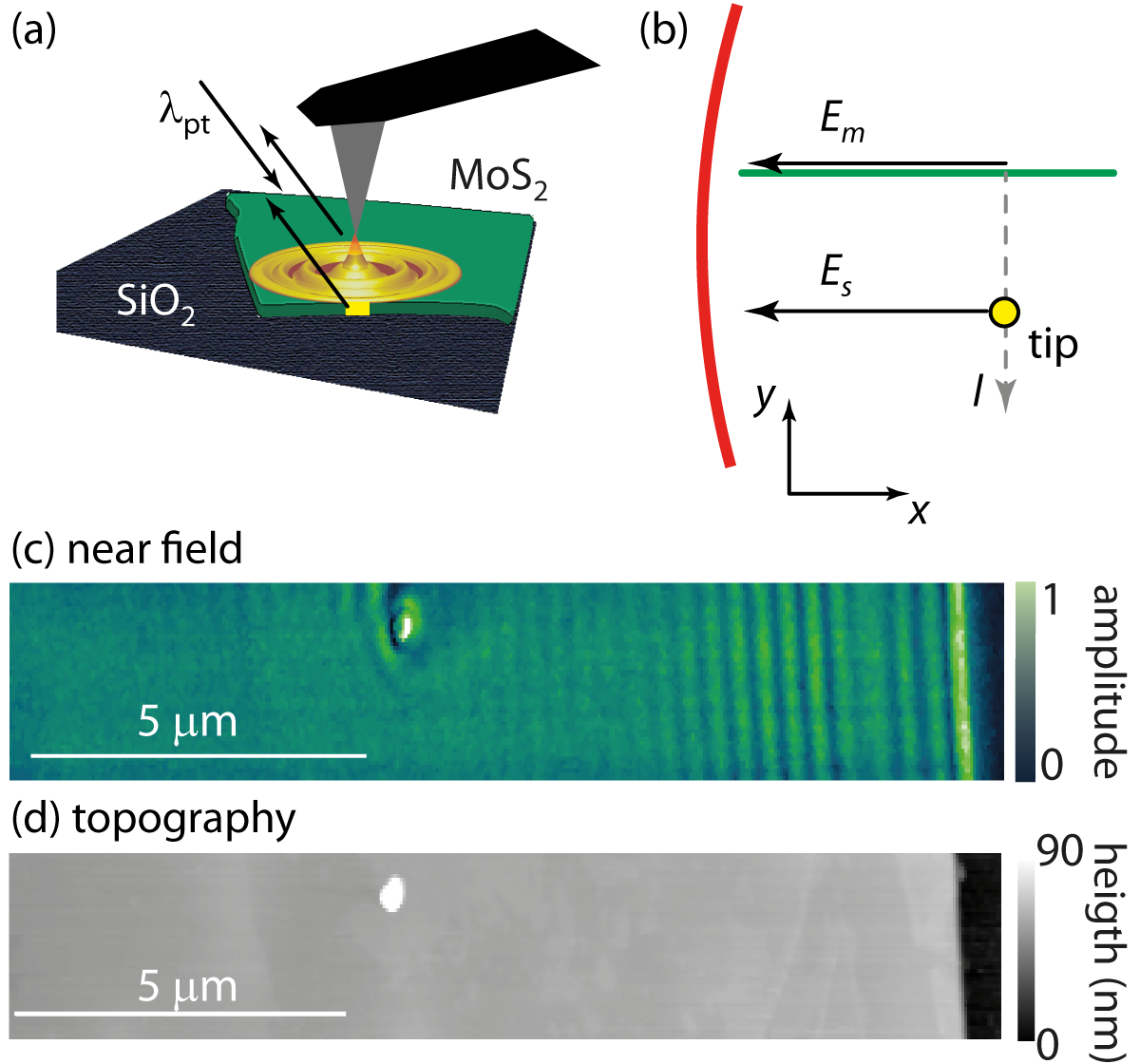
To measure the dispersion of the waveguided modes, we imaged their near-fields on MoS2 flakes using a scattering-type SNOM (s-SNOM, Ref. 37) operating at excitation energies in the visible, Fig 2. Polaritons manifest in near-field images through interference between various scattering pathways in the SNOM. To obtain the dispersion, we repeated the experiment for various excitation wavelengths and determined the polariton wavevector as a function of energy. Such experiments have been reported only for infrared wavenlengths or single-line laser excitation.18; 30; 12 Here, we implement it for visible excitation (up to 540 nm) using a fully tunable, narrow-line, and noise-suppressed laser.
Thin flakes of MoS2 on a Si substrate with 300 nm SiO2 were prepared by mechanical exfoliation. The substrate was sonicated (20-30 min), washed (isopropanol, acetone), and dried under nitrogen gas. We cleaved a piece of MoS2 several times with a scotch tape and then transferred it to the freshly prepared substrate. We examined the size and thickness of the flakes by atomic force microscopy (AFM). The SNOM measurements were conducted on flakes of sub-wavelength thickness that are suitable as waveguides. In this paper we report the results obtained on a flakes with and nm.
In the s-SNOM (neasnom by neaspec) the laser illuminates a metallic AFM tip, Fig. 2a. The tip produces an optical near field that excites slab polaritons in the flake. A mirror collects the light that gets scattered by the tip or emitted by the sample, Fig. 2b. The light is demodulated in a pseudo-heterodyne detection setup (3rd harmonic),38 which produces a near-field image of the sample, Fig. 2c, with characteristic fringes and patterns that we will further analyse below. The AFM topography of the same area, Fig. 2d, is completely flat and featureless. The microscopy images were produced simultaneously using enhanced platinum tips (neaspec) working in tapping mode at the tip eigenfrequency kHz with an amplitude of 50 nm. A unique feature of our s-SNOM system is the wide range of laser wavelengths in the visible 700-450 nm (1.77-2.75 eV) that are provided by the fully tunable C-Wave laser (Hübner Photonics). Similar near-field images as in Fig. 2 were obtained for the energy range 1.79-2.3 eV, which covers the and exciton resonance of MoS2.
There are several mechanisms that can give rise to the interference patterns in Fig. 2c. The dominant interference mechanism when exciting TMDCs in the visible is that edge emitted light with electric field amplitude interferes with light that was scattered directly by the metallic tip , Fig. 2b.18; 36 We worked in a configuration where the emmissive edge is parallel to the optical axis of the collecting mirror as sketched in top view in Fig. 2b (, see Supplementary Information). We chose this configuration, because it is free of systematic errors that arise from the limited knowledge of the exact alignment configuration.18 A near-field image as in Fig. 3c shows the field amplitude of the tip and edge emitted waves . In the configuration and for a tip position at a point along a line perpendicular to the edge, at the detector is given by, see Supplementary Information,
| (4) |
with
| (5) |
and
| (6) |
is the amplitude of the light scattered by the tip and the amplitude of the light emitted at the edge towards the collecting mirror. is the complex wavevector of the exciton polariton propagating along the direction, see Fig. 2b for the coordinate system. Its real part yields the polariton wavelength ; its imaginary part is the damping of the polariton. is the component of the photon in free space.
We extracted line scans perpendicular to the sample edge from the near-field images as in Fig. 2c. The fit with Eq. (4) yields the wavelength and damping of the polariton. Equation (4) is valid only for as in Fig. 2b. The fringe period – i.e., the distance between two interference maxima – deviates rapidly from for any misalignment. We carefully verified the dependence and corrected the measured for the misalignment, see Supplementary Information for details.
IV Results
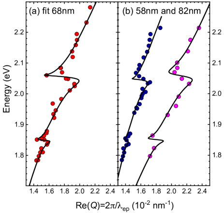
The experimental dispersion of MoS2 flakes with thicknesses below 100 nm shows two backbending slopes around 1.85 and 2.05 eV, see Fig. 3. The backbending is weakest for the thinnest flake with nm. It increases for 68 nm and then again gets weaker for the thickest 82 nm flake. The increase and decrease of the backbending is characteristic of the TM0 mode, Fig 1. We detected no signatures of the TE0 mode in our near-field images. This is reasonable, because the predominantly polarized near field of the metallic tip cannot couple to TE eigenmodes that are polarized in plane. The line in Fig. 3a is a fit to the experimental data obtained at the nm flake with Eq. (2). We used the same parameters, Table 1, to calculate the dispersion for and nm. The fit describes the data obtained in the other two flakes very well, Fig. 3b. In particular, it reproduces the decreasing Rabi splitting for smaller and larger thicknesses.
| (eV) | (meV) | (meV) | (meV) | (meV) | |
|---|---|---|---|---|---|
| A exciton | 1.850 | 11 | 84 | 42 | 1.6 |
| B exciton | 2.053 | 35 | 194 | 97 | 9.4 |
The pronounced backbending of the TM0 dielectric function implies that the and excitons of the MoS2 slabs are in the regime of strong light-matter coupling.1; 32 More importantly, the coupling remains strong between excitons in bulk MoS2 and free-space photons, Table 1. We find a coupling strength meV for the exciton in bulk MoS2 that is four times larger than its damping meV. The coupling strength of the exciton meV exceeds its decay rate meV almost by a factor of three. The Rabi splitting in MoS2 is an order of magnitude larger than in classical semiconductors like GaAs. It rivals the coupling in found in wide band-gap semiconductors with low dielectric constants,5 but the dielectric constants of MoS2 are large. We find an out-of-plane constant and an in-plane background dielectric constant , in good agreement with previous measurements.30; 12 At the same time, the exciton energies eV and eV make MoS2 an attractive material for polariton-based devices at visible and near-infrared wavelengths.5
Interestingly, the exciton polaritons of MoS2 also fulfill the condition for very strong light-matter coupling. Very strong coupling means that the coupling strength is comparable to the exciton binding energy , i.e., .39 To calculate we need the exciton binding energies of bulk MoS2 that, surprisingly, remain debated.21; 11; 14 Depending on the interpretation of the optical spectra meV and meV placing and . For approaching one, light-matter coupling contributes to the interaction between the electron and the hole forming the exciton.39 They start to interact by emitting and absorbing virtual photons, which reduces the exciton radius in the lower and increases the radius in the upper polariton state. The condition for very strong coupling is only met by bulk MoS2 and lost for thin slabs and monolayers, because the coupling decreases to meV (Ref. 16) and the binding energy increases to meV (Ref. 40; 8) so that drops to or less.
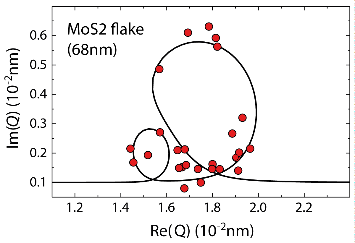
The damping rates and extracted from the fits to the TM0 dispersion are smaller than the inhomogeneous linewidth of MoS2 flakes at room temperature.13; 8 Nevertheless, they most likely underestimate the lifetime of the MoS2 excitons, because we neglected the damping of the photonic mode via edge emission. is three times larger than , which agrees with the range of rates ovwerved for the two excitonic states.28; 27 We can also determine the spatial damping of the MoS2 polaritons from the near-field images, because the interference patterns exist over several micrometers, Fig. 2c. The damping depends strongly on the exciting laser frequency: While the pattern extends for some micrometers for frequencies away from the and exciton, Supplementary Fig. S1, it drops to hundreds of nanometers for resonant excitation. We extract the spatial damping from the fits with Eq. (4). A plot of the imaginary versus the real part of the wavevector in Fig. 4 shows two loops at the wavevector of the excitons in the uncoupled system. The looping shape is another signature of strong coupling in photonic systems confirming the result of the versus plot in Fig. 3.32 We calculated the full line in Fig. 4 using Eq. (2) with the fitting parameters obtained from the polariton dispersion and adding a constant damping of nm-1. The latter represents scattering by crystal imperfections and errors introduced by the experimental setup. With increasing distance between tip and edge the edge emitted photons propagate off the optical axis, which eventually reduces the interference amplitude. The maximum propagation length of 5 m in Fig. 4, therefore, poses a lower bound to the polariton propagation. In resonance with the exciton the propagation length drops to 100 nm, but even this value is longer than for the bulk polariton. Using the parameters of Table 1 we predict a minimum propagation length nm for polaritons at the exciton energies in the bulk. This high damping is a consequence of the strong coupling, because these polariton frequencies correspond to the forbidden gap that opens between lower and upper polariton in the dispersion for real vectors.4; 32 The propagation length far away from resonances in bulk MoS2 is overestimated in our experiments; it should be evaluated in crystals of high quality at low temperatures.
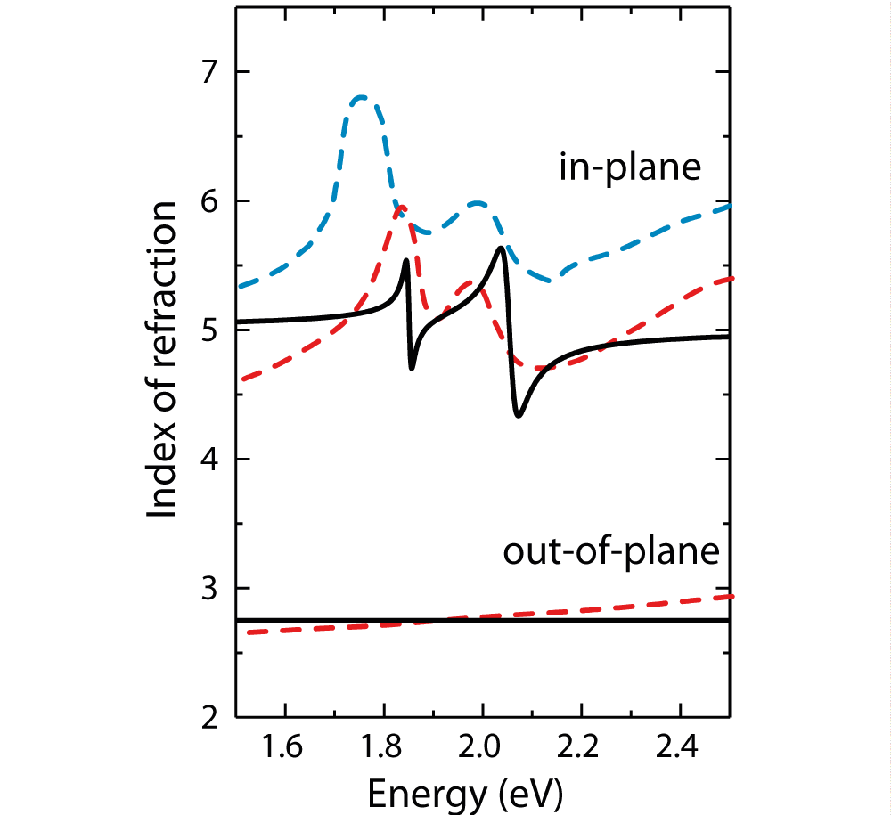
It is instructive to deduce the polariton contribution to the bulk dielectric function in MoS2 from our slab measurements. Figure 5 shows the polaritonic part of the index of refraction compared to reflectance (blue) and ellipsometric (red) measurements on bulk MoS2.11; 12 The overall agreement is quite remarkable confirming that the optical response of MoS2 in the visible is dominated by exciton-related effects. The bulk measurements are much broader in line width than the polaritonic part of the index of refraction. This is due to band to band transitions and defect-related excitations. It would be interesting to obtain more experimental data at low temperatures to better distinguish between intrinsic and extrinsic sources of damping. The similarity between the polaritonic contribution to the index of refraction obtained from the slabs and the experiments on bulk MoS2 show that polaritons need to be considered in the description of this material. We note that the refractive indices in Fig. 5 are strongly anisotropic with a difference between the in-plane and out-of-plane refractive index.11; 12 Polaritons can be guided and confined efficiently along the MoS2 layers even in the bulk material.
V Conclusion
In conclusion, we measured the dispersion of the transverse magnetic modes in slabs of MoS2 using near-field optical microscopy with fully tunable visible excitation. We determined the strength of light-matter coupling in bulk MoS2 from the dispersion of the slab mode. The and exciton are in the regime of strong light-matter coupling with a coupling strength of 40 meV for the and 100 meV for the exciton, which exceeds their losses by more than a factor of two. Because their coupling strength is also comparable to the exciton binding energy, the formation of the exciton and its properties depend also on the coupling to light. MoS2 combines strong light-matter coupling with a large index of refraction and a strong anisotropy in its dielectric response. It is a very promising material for polariton-based devices operating under ambient conditions.
VI Acknowledgements
We acknowledge financial support by the European Research Council (ERC) under grant DarkSERS (772108) and by the German Science Foundation (DFG) within the Priority Program SPP 2244 “2DMP”.
References
- Baranov et al. (2018) Denis G. Baranov, Martin Wersäll, Jorge Cuadra, Tomasz J. Antosiewicz, and Timur Shegai, “Novel nanostructures and materials for strong light-matter interactions,” ACS Photonics 5, 24–42 (2018).
- Frisk Kockum et al. (2019) Anton Frisk Kockum, Adam Miranowicz, Simone De Liberato, Salvatore Savasta, and Franco Nori, “Ultrastrong coupling between light and matter,” Nat. Rev. Phys. 1, 19–40 (2019).
- Yu and Cardona (1996) P. Yu and M. Cardona, Fundamentals of Semiconductor Physics (Springer, Heidelberg, 1996).
- Adreani (1995) L. C. Adreani, “Optical transitions, excitons, and polaritons in bulk and low-dimensional semiconductor structures,” in Confined Electrons and Photons, edited by E. Burstein and C. Weisbuch (Plenum Press, New York, 1995) p. 57.
- Sanvitto and Kéna-Cohen (2016) D. Sanvitto and S. Kéna-Cohen, “The road towards polaritonic devices,” Nat. Mat. 15, 1061 (2016).
- Sun et al. (2008) Liaoxin Sun, Zhanghai Chen, Qijun Ren, Ke Yu, Lihui Bai, Weihang Zhou, Hui Xiong, Z. Q. Zhu, and Xuechu Shen, “Direct observation of whispering gallery mode polaritons and their dispersion in a ZnO tapered microcavity,” Phys. Rev. Lett. 100, 156403 (2008).
- Kang et al. (2019) Jang-Won Kang, Bokyung Song, Wenjing Liu, Seong-Ju Park, Ritesh Agarwal, and Chang-Hee Cho, “Room temperature polariton lasing in quantumheterostructure nanocavities,” Sci. Adv. 5, eaau9338 (2019).
- Wang et al. (2018a) Gang Wang, Alexey Chernikov, Mikhail M. Glazov, Tony F. Heinz, Xavier Marie, Thierry Amand, and Bernhard Urbaszek, “Excitons in atomically thin transition metal dichalcogenides,” Rev. Mod. Phys. 90, 021001 (2018a).
- Munkhbat et al. (2019) B. Munkhbat, D. G. Baranov, M. Stuuhrenber, M. Wersall, A. Bisht, and T. Shegai, “Self hybrized exciton polaritons in multilayers of transition metal dichalcogenides for efficient light absorption,” ACS Photon. 6, 139–147 (2019).
- Hu and Fei (2019) Fengrui Hu and Zhe Fei, “Recent progress on exciton polaritons in layered transition-metal dichalcogenides,” Adv. Opt. Mat. 8, 1901003 (2019).
- Neville and Evans (1976) R. A. Neville and B. L. Evans, “The band edge excitons in 2H-MoS2,” phys. stat. sol. b 73, 597–606 (1976).
- Ermolaev et al. (2020) G. A. Ermolaev, D. V. Grudinin, Y. V. Stebunov, K. V. Voronin, V. G. Kravets, J. Duan, A. B. Mazitov, G. I. Tselikov, A. Bylinkin, D. I. Yakubovsky, S. M. Novikov, D. G. Baranov, A. Y. Nikitin, I. A. Kruglov, T. Shegai, P. Alonso-Gonzalez, A. N. Grigorenko, A. V. Arsenin, K. S. Novoselov, and V. S. Volkov, “Giant optical anisotropy in transition metal dichalcogenides for next-generation photonics,” (2020), arXiv:arXiv:2006.00884 [physics.app-ph] .
- Mak et al. (2010) Kin Fai Mak, Changgu Lee, James Hone, Jie Shan, and Tony F. Heinz, “Atomically thin MoS2: A new direct-gap semiconductor,” Phys. Rev. Lett. 105, 136805 (2010).
- Fortin and Raga (1975) E. Fortin and F. Raga, “Excitons in molybdenum disulphide,” Phys. Rev. B 11, 905 (1975).
- Schneider et al. (2018) Christian Schneider, Mikhail M. Glazov, Tobias Korn, Sven Höfling, and Bernhard Urbaszek, “Two-dimensional semiconductors in the regime of strong light-matter coupling,” Nat. Commun. 9, 2695 (2018).
- Liu et al. (2014) Xiaoze Liu, Tal Galfsky, Zheng Sun, Fengnian Xia, Erh chen Lin, Yi-Hsien Lee, Stephane Kena-Cohen, and Vinod M. Menon, “Strong light–matter coupling in two-dimensionalatomic crystals,” Nat. Photon. 9, 30 (2014).
- Flatten et al. (2016) L. C. Flatten, Z. He, D. M. Coles, A. A. P. Trichet, A. W. Powell, R. A. Taylor, J. H. Warner, and J. M. Smith, “Room-temperature exciton-polaritons with two-dimensional WS2,” Sci. Rep. 6, 33134 (2016).
- Hu et al. (2017a) F. Hu, Y. Luan, M. E. Scott, J. Yan, D. G. Mandrus, X. Xu, and Z. Fei, “Imaging exciton–polariton transport in MoSe2 waveguides,” Nat. Photon. 11, 356 (2017a).
- Savona et al. (1995) V. Savona, L. C. Andreani, P. Schwendimann, and A. Quattropani, “Quantum well excitons in semiconductor microcavities: Unified treatment of weak and strong coupling regimes,” Sol. Stat. Commun. 93, 733–739 (1995).
- Manceau et al. (2017) J-M. Manceau, G. Biasiol, N. L. Tran, I. Carusotto, and R. Colombelli, “Immunity of intersubband polaritons to inhomogeneous broadening,” Phys. Rev. B 96, 235301 (2017).
- Saigal et al. (2016) N. Saigal, V. Sugunakar, and S. Ghosh, “Exciton binding energy in bulk MoS2: A reassessment,” Appl. Phys. Lett. 108, 132105 (2016).
- Carvalho et al. (2015) Bruno R. Carvalho, Leandro M. Malard, Juliana M. Alves, Cristiano Fantini, and Marcos A. Pimenta, “Symmetry-dependent exciton-phonon coupling in 2D and bulk MoS2 observed by resonance Raman scattering,” Phys. Rev. Lett. 114, 136403 (2015).
- Moody et al. (2015) Galan Moody, Chandriker Kavir Dass, Kai Hao, Chang-Hsiao Chen, Lain-Jong Li, Akshay Singh, Kha Tran, Genevieve Clark, Xiaodong Xu, Gunnar Berghauser, Ermin Malic, Andreas Knorr, and Xiaoqin Li, “Intrinsic homogeneous linewidth and broadening mechanisms of excitons in monolayer transitionmetal dichalcogenides,” Nat. Commun. 6, 8315 (2015).
- Cadiz et al. (2017) F. Cadiz, E. Courtade, C. Robert, G. Wang, Y. Shen, H. Cai, T. Taniguchi, K. Watanabe, H. Carrere, D. Lagarde, M. Manca, T. Amand, P. Renucci, S. Tongay, X. Marie, and B. Urbaszek, “Excitonic linewidth approaching the homogeneous limit in MoS2-based van der Waals heterostructures,” Phys. Rev. X 7, 021026 (2017).
- Shi et al. (2013) Hongyan Shi, Rusen Yan, Simone Bertolazzi, Jacopo Brivio, Bo Gao, Andras Kis, Debdeep Jena, Huili Grace Xing, and Libai Huang, “Exciton dynamics in suspended monolayer and few-layer MoS2 2D crystals,” ACS Nano 7, 1072–1080 (2013).
- Palummo et al. (2015) Maurizia Palummo, Marco Bernardi, and Jeffrey C. Grossman, “Exciton radiative lifetimes in two-dimensional transition metal dichalcogenides,” Nano Lett. 15, 2794–2800 (2015).
- Cha et al. (2016) Soonyoung Cha, Ji Ho Sung, Sangwan Sim, Jun Park, Hoseok Heo, Moon-Ho Jo, and Hyunyong Choi, “-intraexcitonic dynamics in monolayer MoS2 probed by ultrafast mid-infrared spectroscopy,” Nat. Comm. 7, 10768 (2016).
- Wang et al. (2018b) Ting Wang, Yirui Zhang, Yuanshuang Liu, Junyi Li, Dameng Liu, Jianbin Luo, and Kai Ge, “Layer-number-dependent exciton recombination behaviors of MoS2 determined by fluorescence-lifetime imaging microscopy,” J. Phys. Chem. C 122, 18651–18658 (2018b).
- Sell et al. (1973) D. D. Sell, S. E. Stokowski, R. Dingle, and J. V. DiLorenzo, “Polariton reflectance and photoluminescence in high-purity GaAs,” Phys. Rev. B 7, 4568 (1973).
- Hu et al. (2017b) D. Hu, X. Yang, C. Li, R. Liu, Z. Yao, H. Hu, S. N. Gilbert Coder, J. Chen, Z. Sun, M. Liu, and Q. Dai, “Probing optical anisotropy of nanometer-thin van der Waals microcrystals by near-field imaging,” Nat. Commun. 8, 1471 (2017b).
- Khurgin (2015) J. B. Khurgin, “Two-dimensional exciton–polariton—light guiding by transition metal dichalcogenide monolayers,” Optica 2, 740 (2015).
- Wolff et al. (2018) Christian Wolff, Kurt Busch, and N. Asger Mortensen, “Modal expansions in periodic photonic systems with material loss and dispersion,” Phys. Rev. B 97, 104203 (2018).
- Arakawa et al. (1973) E. T. Arakawa, M. W. Williams, R. N. Hamm, and R. H. Ritchie, “Effect of damping on surface plasmon dispersion,” Phys. Rev. Lett. 31, 1127 (1973).
- Henry and Hopfield (1965) C. H. Henry and J. J. Hopfield, “Raman scattering by polaritons,” Phys. Rev. Lett. 15, 964 (1965).
- Mueller et al. (2020) N. S. Mueller, Yu Okamura, Bruno G. M. Vieira, Sabrina Juergensen, Holger Lange, Eduardo B. Barros, Florian Schulz, and Stephanie Reich, “Deep strong light-matter coupling in plasmonic nanoparticle crystals,” Nature 580, 780 (2020).
- Fei et al. (2016) Z. Fei, M. E. Scott, D. J. Gosztola, IV J. J. Foley, J. Yan, D. G. Mandrus, H. Wen, P. Zhou, D. W. Zhang, Y. Sun, J. R. Guest, S. K. Gray, W. Bao, G. P. Wiederrecht, and X. Xu, “Nano-optical imaging of WSe2 waveguide modes revealing light-exciton interactions,” Phys. Rev. B 94, 081402 (2016).
- Taubner et al. (2003) T. Taubner, R. Hillenbrand, and F. Keilmann, “Performance of visible and mid‐infrared scattering‐type near‐field optical microscopes,” J. Microscopy 210, 311–314 (2003).
- Hillenbrand et al. (2001) R. Hillenbrand, B. Knoll, and F. Keilmann, “Pure optical contrast in scattering‐type scanning near‐field microscopy,” J. Microscopy 202, 77–83 (2001).
- Khurgin (2001) J. B. Khurgin, “Excitonic radius in the cavity polariton in the regime of very strong coupling,” Sol. Stat. Commun. 117, 307 (2001).
- Zhang et al. (2014) Chendong Zhang, Amber Johnson, Chang-Lung Hsu, Lain-Jong Li, and Chih-Kang Shih, “Direct imaging of band profile in single layer MoS2 on graphite: Quasiparticle energy gap, metallic edge states, and edge band bending,” Nano Lett. 14, 2443 (2014).