Circuit quantum electrodynamics (cQED) with modular quasi-lumped models
Abstract
Extracting the Hamiltonian of interacting quantum-information processing systems is a keystone problem in the realization of complex phenomena and large-scale quantum computers. The remarkable growth of the field increasingly requires precise, widely-applicable, and modular methods that can model the quantum electrodynamics of the physical circuits, including their more-subtle renormalization effects. Here, we present a computationally-efficient method satisfying these criteria. The method partitions a quantum device into compact lumped or quasi-distributed cells. Each is first simulated individually. The composite system is then reduced and mapped to a set of simple subsystem building blocks and their pairwise interactions. The method operates within the quasi-lumped approximation and, with no further approximation, systematically accounts for constraints, couplings, parameter renormalizations, and non-perturbative loading effects. We experimentally validate the method on large-scale, state-of-the-art superconducting quantum processors. We find that the full method improves the experimental agreement by a factor of two over taking standard coupling approximations when tested on the most sensitive and dressed Hamiltonian parameters of the measured devices.
Quantum phenomena offer a distinct advantage for information processing, assuming we can faithfully design and realize the physical systems underlying them. A leading platform to accomplish this goal has emerged in the form of superconducting quantum technology (Devoret and Schoelkopf, 2013; Gambetta et al., 2017; Krantz et al., 2019; Kjaergaard et al., 2020; Blais et al., 2020), which employs macroscopic, lithographically-defined, and configurable devices. Their design versatility, however, comes with inherent challenges—parameter variability, a complicated design space, and the difficulty of engineering their non-linear interactions. These challenges pose a concern of central importance for the growth of the field and have received a strong and growing interest in the form of new design and quantization methods (Nigg et al., 2012; Bourassa et al., 2012; Solgun et al., 2014; Solgun and DiVincenzo, 2015; Smith et al., 2016; Malekakhlagh and Türeci, 2016; Gely et al., 2017; Malekakhlagh et al., 2017; Pechal and Safavi-Naeini, 2017; Minev et al., 2018; Parra-Rodriguez et al., 2019, 2018; Ansari, 2019; Krupko et al., 2018; Malekakhlagh et al., 2020a; Solgun et al., 2019; Petrescu et al., 2019; You et al., 2019; Di Paolo et al., 2019; Gely and Steele, 2020; Ding et al., 2020; Kerman, 2020; Minev et al., 2020; Kyaw et al., 2020; Malekakhlagh et al., 2020b; Menke et al., 2021). The rapidly growing pace of diversity, complexity, and scale of quantum hardware (Wallraff et al., 2004; Paik et al., 2011; Barends et al., 2013; Minev et al., 2013; Yan et al., 2016; Brecht et al., 2016; Rosenberg et al., 2017; Versluis et al., 2017; Naik et al., 2017; Charles James Neill, 2017; Yan et al., 2018; Minev et al., 2019; Antonio D. et al., 2021) urges for methods that are increasingly modular, widely-applicable, yet ever-more precise. As such, these methods must closely incorporate details of the layout, materials, and electromagnetic environment of the physical device, while keeping approximations to a minimum without sacrificing computational efficiency.
Here, we develop such a precise, modular method that operates at the physical-device level and that is suitable for a wide array of quantum devices. The method builds on the quantization of lumped models (Yurke and Denker, 1984; Devoret, 1995; Burkard et al., 2004), which is more computationally efficient than full-wave methods (Nigg et al., 2012; Solgun and DiVincenzo, 2015; Minev et al., 2020). The method also handles distributed resonant structures, such as co-planar waveguide (CPW) resonators. Modularity is achieved in two ways. First, the physical layout of the quantum device is systematically partitioned into disjoint cells—physical blocks of the device. Each cell can be independently simulated to extract its electromagnetic parameters. Second, the effective circuit of the device is partitioned into non-dynamical coupler elements and nodes and into subsystem building blocks. A subsystem is selected based on two requirements: i) it should constitute a well-understood, basic system in isolation and ii) it should have sufficient parameter flexibility. The latter enables the faithful reduction and mapping of the larger device into subsystems, without loss of information. The larger device model is stitched together from the results of the cell simulations. It is then reduced according to the subsystem partitions. In the process, constraints and non-dynamical degrees of freedom associated with the coupling structures are systematically eliminated; dressing of the systems and their interactions because of this are accounted for. The reduction is precise in that no approximations are made. All dressing and effective parameter renormalizations of the subsystems are tracked, which are mediated by the coupling structures.
We experimentally tested the method on two large-scale, superconducting quantum processors (Antonio D. et al., 2021), which employed transmon qubits (Koch et al., 2007) and CPW structures. Each qubit was connected to four or five neighboring structures, spanning a wide range of coupling strengths. We observed renormalizations on the order of 25% for subsystem Hamiltonian parameters due to coupling dressing and a series of smaller renormalizations due to unwanted, indirect couplings and higher-order effects. We provide a detailed budget to account for the extent to which each model parameter influenced the results. We compare the full method presented here to one that resorts to standard approximations, weak coupling and no dressing of spatial eigenfields. The full method presented here yields a factor of two improvement on the experimental agreement. The method is applicable to the analysis of a broad class of quantum processors. We have automated it in the open-source project Qiskit Metal | for quantum device design 111For an early version of the open-source code (Minev et al., 2021) developed by the authors of this manuscript, see qiskit.org/metal. The Qiskit Metal project builds on github.com/zlatko-minev/pyEPR..
I Partitioning a quantum device into interconnected component cells
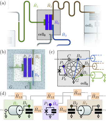
The physical layout of a quantum information processor, such as the one depicted in Fig. 1(a), can be thought of as the interconnected collection of quasi-independent subsystems and inter-system couplers. Each subsystem is identified with a domain of the physical layout and supports a set of quantized, potentially-anharmonic modes. When considered in isolation, a subsystem could be one that is well understood and whose parameters could be readily obtainable, using analytical or numerical techniques. However, due to its embedding in the larger device network and loading by system-system coupling structures, its properties can be dressed and can significantly depend on parts of the larger network. Generally, this dressing of the Hamiltonian parameters is necessarily unavoidable and non-local. Even for relatively moderate non-linear coupling strengths, the renormalizations of the effective subsystem Hamiltonian and its spectrum can be significant; for an experimental example of a large, 1 GHz mode dressing, see Sec. IV. Similarly, the interaction between two subsystems is dressed in a potentially non-local manner that can depend on more than the immediate coupling structure and can be influenced by the physical layout more broadly. Faithfully and systematically accounting for such effects in the increasingly complex physical device layouts is important for improved experimental agreement, see Fig. 4.
To capture these effects, we aim to systematically and modularly study the physical device layout by partitioning it into disjoint cells, see Fig. 1(b). Each cell is first analyzed quasi-analytically or using numerical quasi-static electromagnetic methods to extract device parameters used to construct the full system Hamiltonian. Importantly, cells do not correspond to subsystems, see Sec. II. A semi-classical model of the connected system is constructed and reduced to a simpler, dressed model of the device, see Fig. 1(b) and 1(c).
For a subsystem coupled to neighbors, we explicitly construct the composite-system Hamiltonian , within the quasi-lumped approximation but with no further approximations, in the pair-wise interaction form,
| (1) |
where and are the dressed Hamiltonians of the subsystem and its -th neighbor, respectively, and is the dressed, bi-linear interaction Hamiltonian between the -th and -th systems.
In the construction, the -th and -th system Hilbert spaces are disjoint; hence, . Nonetheless, their dressed Hamiltonians and are interdependent in terms of their parameters and physical layouts—due to the coupling structures and dressing by the larger network.
The dressed interaction Hamiltonian of the -th and -th systems is
| (2) |
where the effective coupling capacitance and inductance are and , respectively, and the generalized charge and magnetic flux operators of the -th and -th systems involved in the coupling are , , , and . For systems coupled by multiple physical degrees of freedom, see the more general form of Eq. (2) obtained in Eqs. (12) and (13).
In the case of purely capacitive inter-system coupling (i.e., ), we conveniently reexpress the interaction in terms of the dimensionless operators and , scaled by the choice scaling factors and ,
| (3) |
where the linear coupling energy . When operating with continuous quadrature variables, such as , and employing a harmonic basis, one typically employs the zero-point quantum fluctuations of the quadrature with respect to the linearized system; i.e., . Sometimes in the case of a transmon qubit (Koch et al., 2007), especially when interested in charge effects, one operates with wrapped or discrete-variable quadratures. In the case of the discrete-variable Cooper pair number operator , the scaling is , where is the elementary electron charge.
Before proceeding to the general treatment and explicit construction of Eqs. (1)–(5), for definitiveness of example, consider the device and associated reduction steps depicted in Fig. 1. The dressed Hamiltonian of the system, a co-planar-waveguide (CPW) resonator, is , see Sec. III. Due to the coupling and network dressings, the normal mode frequencies , annihilation operators , and associated zero-point-quantum fluctuations of the physical degrees of freedom are not dependent solely on the geometry and materials of the CPW structure. They additionally include contributions arising from the coupler structure and transmon qubit self-capacitance. Similarly, the qubit system frequency of is weakly interdependent with due to the semi-classical hybridization; i.e., when one tunes , one has to be careful to also retune for maximum accuracy. The coupling parameters and are dressed not only by the -th and -th systems, but also by couplers coupling the -th system to its other neighbors; e.g., the qubit-bus coupling can weakly influence the qubit-readout coupling.
In the following section, we capture these potentially non-perturbative effects, see Sec. III. Such a detailed construction is required to treat larger and higher-order coupling effects and to obtain improved experimental agreement, see Sec. IV. Additionally, effects such as impurity scattering on the distributed CPW structures are accounted for—this is the cavity-QED equivalent of a gauge-dependent diamagnetic contribution (Malekakhlagh and Türeci, 2016).
II Theory of the composite model
In this section, we present the theory of the general construction of Eqs. (1) and (2) starting from the analysis of disjoint partitions of the physical device layout. The model is constructed to allow the mapping of the larger interconnected network to a set of small, independent, subsystem building blocks—each potentially well understood in isolation. Each such cell partition can be independently simulated, thus decoupling the complexity of the network and providing modular simulations for improved computational efficiency. From the results of these independent simulations, we construct the composite-system Lagrangian and then the quantum Hamiltonian of the systems and interactions. In the process, we eliminate holonomic constraints and non-dynamical, coupling degrees of freedom, and account for their dressing of the systems and couplings. The treatment in this section, for generality, is more formal and abstract. However, in practice, significant simplifications occur due to the typically diagonal, block, or sparse structure of the circuit matrices.
We simultaneously employ two different types of partitions of the device. The first partitions the physical layout of the device into strictly disjoint cell modules—each of which can be independently simulated or analyzed to extract effective circuit parameters. The second partition operates at the level of the effective quasi-lumped schematic of the device. It partitions the device network nodes and elements into subsets of each. One of the subsets is for all non-system couplers. The remaining are for the subsystems. The cell and system partitions of the composite circuit are distinct from each other. This is illustrated by the qubit cell of Fig. 1(b). It incorporates the transmon qubit elements (metal pads and in a cutout of the ground plane ) but also elements from three neighboring non-qubit systems (structures and ).
Let and denote the sets of all nodes and elements in the device network, respectively. To partition into cells, the elements of are disjointly distributed among sets. The nodes in are however distributed among sets with potential overlap. If we denote the set of all non-datum nodes assigned to the -th cell as , then , where is the single-element set comprising just the circuit datum (ground node). The intersection can be non-empty. Each cell can incorporate the datum. To partition into subsystems, and are broken up into strictly disjoint sub-sets. If denotes the set of all non-datum nodes assigned to the -th system and denotes the set of all non-system, non-datum nodes, then , where for . In the case of a continuous subsystem, comprises a continuum of nodes.
The assignment of nodes and elements to a subsystem is determined by the design intention to realize quasi-independent subsystems, incorporating dynamical degrees of freedom that support quantized modes. A subsystem can also incorporate non-dynamical nodes and zero-frequency modes; e.g., a transmission line open at both ends. The system’s non-dynamical degrees will be preserved in the following reduction. This feature provides helpful flexibility that allows the mapping of the larger network to a set of known building blocks.
A second, necessary condition for a subsystem is that it admits sufficient parameter flexibility in its definition. It must be able to admit the renormalization of the larger network. For example, the simple, ideal transmission line is not a suitable subsystem candidate. It cannot admit in its homogenous construction the inhomogeneity introduced by the impurity scattering effect of a coupler structure. The line must be allowed to incorporate the inhomogeneity in line parameters due to the coupler structure in its definition; see Fig. 2 for an example.
Nodes and elements not part of any subsystem are assigned to the coupler sets. The coupler nodes should all be non-dynamical—they do not support quantized modes on their own. A sufficient condition to identify a non-dynamical node is that it is touched by only inductive or capacitive elements, but not by elements of both classes.
Inductive elements can be linear or non-linear. A non-linear inductive dipole is a two-terminal purely-inductive sub-circuit, such as a Josephson tunnel junction, flux-biased SQUID (Zimmerman and Silver, 1966; Clarke and Braginski, 2004), SNAIL (Frattini et al., 2018), or a more complicated composite sub-circuit. We describe such dipoles using the formulation of Ref. Minev et al., 2020. The -th non-linear dipole is fully characterized by a known energy function of the generalized magnetic flux across it and any external bias parameters , such as the magnetic flux of a d.c. voltage bias. The dipole can also have an intrinsic capacitance that spans its two terminals. The energy function of the dipole intrinsic capacitance is .
With respect to the circuit operating point (Minev, 2019; Minev et al., 2020), one can partition the inductive energy into strictly linear and non-linear contributions
| (4a) | ||||
| (4b) | ||||
respectively, where is the linear-response inductance of the dipole at the bias point. For example, for a SQUID dipole, , where is the effective Josephson energy as a function of the bias and . For a Josephson tunnel junction, is simply the Josephson inductance, which can be computed from the Ambegaokar-Baratoff expression and room-temperature resistance measurements of the junction (Gloos et al., 2000). Henceforth, we make the bias argument implicit.
The energy functions of the non-linear dipoles and the structure and topology of the cells are known. The circuit parameters of the linear elements contained in can be extracted using analytical results (Wolff, 2006) or numerical techniques, see Sec. II.2. Information about the linear part of the circuit of the -th cell can be organized in the cell’s geometric capacitance and inverse inductance matrices and , respectively. We define these matrices with respect to the node-to-datum generalized magnetic fluxes of the circuit (Devoret, 1995; Minev et al., 2020). In the case of a cell that can be considered in the lumped regime, is the reduced Maxwell capacitance matrix, see Eq. (15). In this case, represents a fully connected graph, see Fig. 1(c).
We incorporate and of the non-linear dipoles into and to define the total cell linear capacitance and inverse inductance matrices. In terms of these, the capacitance and inverse inductance matrices of the composite-system are
| (5) |
respectively. They are real, symmetric, and nearly block diagonal. The matrix is guaranteed to be positive semi-definite, but due to the inclusion of , does not have this guarantee. Typically, is sparse and rank deficient. In terms of system, not cell, partitions, and have a simple block structure. All subsystems are described by blocks in the diagonals of and . The only off-diagonal blocks in the two matrices are due to coupling elements spanning subsystems. Coupler nodes also introduce diagonal blocks in the two matrices.
To describe the physical model, we introduce the column vector of all node-to-datum fluxes , each entry of which is associated with one unique node of . The Lagrangian of the composite system is
| (6) |
where denotes the total number of non-linear dipoles in the network. The Lagrangian is potentially singular due to the rank deficiency of and that of . The singularity leads to dynamics on a constrained submanifold of phase space. In quantization, it is this reduced, constrained phase space that provides the required physical Poisson structure required for canonical quantization (Dirac, 1982).
Before eliminating the coupler constraints on the phase space associated with , we first rotate the Lagrangian basis to place all non-linear dipole fluxes explicitly in the basis. The flux of the -th dipole , where and are the node-to-datum fluxes of its two nodes. We construct the simple, linear transformation with elements in to rotate the basis according to such that explicitly contains all junction fluxes . In the basis , the transformed capacitance and inverse inductance matrices are and , respectively.
To eliminate constraints due to the singularity of , we select all coupler fluxes or linear combinations of fluxes in the kernel space of . For example, these include the fluxes associated with all nodes in that have only capacitive elements touching them. We construct the matrix formed by joining the flux vectors defined in the basis as . The flux-vector image space of is a non-dynamical subspace of the inductors; i.e., , where is the matrix of all zeros. The image space of is not necessarily the full kernel space of ; i.e., .
We purposefully do not fully reduce the dynamics to only the image space of at this stage. This allows the composite network model to be reduced to known subsystems. These subsystems, treated as building blocks of the device, can themselves incorporate a singular Lagrangian. A simple example is that of the open-ended transmission line, which effectively has one less inductor than capacitor and hence a kernel space of with dimension one, which leads to one zero-frequency solution. To map to this known problem, which itself handles its own singularity, we retain the singularity in its definition by not including the associated subspace in the span of .
We denote the complement of as , an matrix whose image is the image space of together with subspace of the kernel of that is not spanned by ; i.e., . Its columns can be selected mostly if not entirely from those of the identity matrix.
We partition the degrees of freedom of the composite system into the non-dynamical degrees of freedom and the remaining ones . For the non-dynamical coordinates, we impose the standard zero initial condition , where denotes the initial time of the circuit and is the length- column vector of all zeros. Using this, we solve for the degrees comprising in terms of the reduced dynamical degrees , and find . In the reduced basis, the reduced capacitance and inverse inductance matrices are
| (7a) | ||||
| (7b) | ||||
respectively. The matrix can be seen as a Schur complement.
In Eq. (7), we have eliminated the holonomic constraints presented by inductive coupler nodes and contracted the problem from to degrees of freedom . The reduction of the coupler nodes renormalizes system parameters subject to the transformation and Eq. (7). In particular, the effective capacitance matrix can be strongly dressed, due to the term containing . This is only a first dressing. The capacitance matrix can be dressed two more times in the following.
The second renormalization step parallels the first, but this time with the roles of the capacitance and inductance matrices flipped. Namely, if there are coupler flux combinations in the kernel space , we repeat the above basis partition protocol to eliminate these with respect to (rather than , as above). An example of a coupler flux in is the flux of a coupler node that is only touched by inductors and no capacitors. Since the steps repeat, for brevity, we do not explicitly detail the process again. Instead, we proceed by assuming the step has been carried out, all coupler nodes in and in have been eliminated. To avoid new notation, we redefine , and to denote in the following the doubly reduced flux basis vector and circuit matrices and to denote the length of .
The generalized, reduced charge vector is . We employ canonical Dirac quantization (Dirac, 1982), explicated in App. C of Ref. Minev et al., 2020, with the canonical commutator , where is the identity matrix of dimension and is the identity operator on the composite-system Hilbert space. The Hamiltonian of the composite system is
| (8) |
where is the reduced effective capacitance matrix with all non-linear dipole inductance contributions subtracted out. Since we included the non-linear dipole fluxes in the basis , this amounts to a simple subtraction of the inductances from the diagonal of . The inversion of the composite-system capacitance matrix leads to the third capacitive dressing of the subsystem parameters by the couplers and coupled systems.
Equation (8) brings us to the desired composite-system Hamiltonian defined by Eqs. (1) and (2). The -th subsystem Hamiltonian is a partition of the matrix equation given in Eq. (8),
| (9) |
where is the set of non-linear dipoles belonging to the -th subsystem. The total number of junctions is . The vectors of subsystem charge and flux operators are
| (10) |
where the function yields the matrix partition of its first argument with respect to the set of nodes indicated in its second argument. Similarly, the -th subsystem matrices are the matrix partitions with respect to the set of nodes of the -th system,
| (11a) | ||||
| (11b) | ||||
where the second and third argument indicates the set of nodes associated with the matrix rows and columns, respectively. The pair-wise interaction terms among the subsystems take the form
| (12) |
where the indices and label the subsystems, for . The effective coupling capacitance and inductance associated with the -th and -th node of the -th and -th subsystems, respectively, are obtained from the off-diagonal blocks of the dressed system matrices,
| (13a) | ||||
| (13b) | ||||
where and denote the single-element subsets of and that comprise just the -th and -th node of the sets, respectively.
By construction, we have assumed that the subsystem Hamiltonians are of familiar, known structure and can be diagonalized by known analytical or numerical methods. For instance, each Hamiltonian can be expressed in a harmonic-oscillator basis and fully diagonalized, as detailed in the methodology of the energy-participation-ratio method (Minev et al., 2020). A diagonalization in this second quantized basis can provide the -th system Hamiltonian in the diagonal form
| (14) |
where is the -th Hamiltonian energy level of the -th resonant eigenmode of the -th subsystem, which supports a total of number of quantized resonant modes. Since we have partitioned the composite into small, manageable subsystems, for an effectively lumped subsystem of interest one can diagonalize independently from the circuit using analytical or numerical techniques. In the case of numerics, one can use a large, truncated basis for the diagonalization, but subsequently can retain only a handful of the low-energy levels. The flux and charge operators can be constructed in this truncated eigenbasis; i.e., in terms of the and eigenstates. Thus, the interaction and composite Hamiltonian can be expressed more efficiently 222This is the form employed in a recent package entitled scqubits; see also Ref. Kerman, 2020..
In this section, we explicitly constructed the subsystem Hamiltonians and their interactions and eliminated all coupler degrees of freedom and associated constraints, and incorporated all circuit effects, such as the diamagnetic contribution, in Eqs. (8)–(13). The parameters of each subsystem Hamiltonian were obtained by three sequential dressings. Thus, the spectrum of and are not circuit parameter independent in general. They can be dressed by their couplers and by each other’s circuit parameters. The dressing can in principle be rather non-local. This depends on the particulars of the circuits. In typical situations, nodes in the network graph separated by a minimal path of several edges can be coupled but potentially negligibly so. For example, in the inversion step of , these distance direct couplings are allowed but severely dampened by the weight of the inversion. However, dressing of node parameters by proximal coupler edges can be large. For example, for the direct capacitance between the pads of a transmon qubit can be renormalized by a factor of two subject to a large pad coupler, such as featured in our experiment, see Sec. IV. The coupling terms are also similarly dressed by the system parameters. Proper elimination at the composite level, rather than at the individual-system level, is essential for more general circuits and accurate results, as observed from data for the theory versus experiment comparison presented in Sec. IV.
II.1 Example of the experimentally measured devices
Let us briefly illustrate the method by returning to the example of Fig. 1. The composite system is comprised of the qubit (), CPW readout resonator (), two CPW bus resonators ( and ), and coupler nodes (); the ellipses in the sets indicate the continuum of nodes associated with the distributed lines. Here, ; however, we only need one lumped simulation cell. This cell contains the set of nodes ; the ground node is considered accessible by every cell. The remaining three cells associated with the bodies of the CPW transmission lines need not be simulated explicitly since they can be handled quasi-analytically, see Sec. III. Following the procedure outlined in Sec. II.2, the cell capacitance matrix is extracted; its fully-connected graph is depicted with green lines in Fig. 1(c). For our experiment, we employed the Ansys Q3D Extractor quasi-field solver. The creation of the qubit cell and extraction of its Maxwell matrix was automated using Qiskit Metal (Minev et al., 2021).
The inductance matrix of the qubit cell contains a single inductor due to the one junction in the cell; i.e., , and for , where the junction flux is . The CPW cells all have diagonal capacitance matrices , where ; their inductance matrices each have a one-dimensional kernel space. The qubit cell inductance matrix in isolation has columns but has unity rank. Since the three bus nodes are touched by inductors in other systems, these three nodes will not be eliminated; i.e., one should consider the kernel space of the composite inductance matrix and not just that of a given cell , see Eq. (5).
Since there are no coupling inductors, we can obtain the reduced Hamiltonian matrices and directly from Eq. (7), without having to perform a second elimination of inductive coupling nodes. Since the transmission line systems have diagonal node-to-datum cell matrices, it suffices to only invert and reduce to obtain all needed information comprised in . The reduced effective circuit is depicted in Fig. 1(d); the third bus is omitted from the illustration for the sake of visual simplicity. The dressed transmon qubit Hamiltonian, associated circuit shaded in green in Fig. 1(d), is
where we have included a potential charge offset , which could be due to a charge fluctuation on any of the nodes in , where , and . Importantly, comprises the dressed and renormalization effect of all capacitances in the qubit cell model; i.e., while we may refer to it as the dressed qubit capacitance, its value depends on the coupling and transmission-line end-loading capacitances. That is, the qubit and the neighboring system Hamiltonians are dressed by each others’ elements and their parameters are not strictly independent. This first dressing is purely classical and due to linear effects. The dressed loading capacitance of the -th line, see Eq. (16), is
The interaction Hamiltonian between the -th and -th subsystems is
where and is the appropriately scaled off-diagonal term of the reduced and inverted , see Eq. (13). In Sec. IV, we compare the parameters of interest found from this method to those experimentally measured on a large-scale quantum processor (Antonio D. et al., 2021).
II.2 Lumped cell model
In the physical model of a lumped cell, see for example Fig. 1(b), each galvanically-isolated conducting island is represented by a node in the circuit. The effect of the geometry and all other physical aspects of the cell, such as dielectric permittivities and material properties, on the electrostatics of the cell are succinctly expressed in the Maxwell capacitance matrix(Zangwill, 2012) , which is reviewed in App. A. The -th off-diagonal element of the Maxwell matrix is the mutual capacitance between the -th and -th node in the cell times negative unity. It is efficiently extracted from the cell model using a quasi-field solver, such as Ansys Q3D Extractor; this process is automated in our open-source project Qiskit Metal (Note, 1). The cell capacitance matrix with respect to the cell node-to-datum generalized magnetic fluxes, see Eqs. (5) and (A1), is
| (15) |
where , is the zero column vector of length , and is the identity matrix of dimension , where .
III Quantum physics of the loaded transmission-line cell
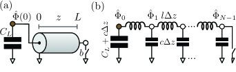
Because of its practical and central importance, we revisit the diagonalization of an end-loaded transmission line, depicted in Fig. 2(a). Quantizing its discrete model and taking the continuous limit, one finds its quantum Hamiltonian
| (16) |
where is the effective end-loading capacitance to ground at , the total charge operator at is , and and are the line total length, capacitance and inductance per unit length, and the charge-density and magnetic-flux-field operators at length along the line, respectively. Due to the end-singularity in the capacitance per unit length of the line, strictly speaking, there is no operator ; hence, the integration from in the lower integral bound, which excludes zero. The scalar, one-dimensional quantum fields obey and , where is the identity operator.
Boundary conditions.
For an open (short) right-end termination, the right boundary condition is of the standard Dirichlet (respectively, Neumann) type, (resp., ). However, the left-end boundary condition is non-standard. It is not of the type covered by standard Sturm–Liouville theory, . This condition makes the boundary condition eigenvalue-dependent leading to transcendental eigensolutions. The equation of motion in the interior of the line is the standard wave equation, valid on , where the phase velocity is .
Characteristic eigenvalue equation.
The Hamiltonian is diagonalized using harmonic solutions and the superposition principle for linear systems. It is easier to show by demoting the problem to classical fields, then recovering the quantum field operators and their quantum zero-point fluctuations using the energy-participation-ratio method (Minev et al., 2020); this establishes the classical-quantum correspondence of the problem and avoids technical detail regarding the proper orthonormalization of the field eigensolution in the presence of the loading irregularity. Using the harmonic ansatz and eliminating and , we find the characteristic eigenvalue equation for ,
| (17) |
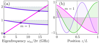
where (resp., for an open (resp., short) right-end boundary condition and . The non-negative integer labels the discrete, uncountable number of modes. The associated spatial phase shift and wavenumber are and , respectively.
The equation is transcendental. For a loading knee frequency (resp., ) the loading capacitor acts as an open (resp., short), while for of the same order of magnitude as , the loading exerts a significant renormalization on the eigenfrequency and eigenfields away from those obtainable from the unloaded transmission line solutions; see Fig. 3. In other words, in this regime, the naive eigenfunctions of an unloaded transmission line are not a good starting-point basis choice, since the phase shift and renormalization of the mode frequencies can be large. It is this latter regime that is experimentally relevant for the devices and measurements presented in Sec. IV. For our devices, the renormalization of the loading was on the order of 20–25%.
Quantum Hamiltonian.
Exploiting the eigensolutions of Eq. (17), in second quantization, Eq. (16) becomes
where is the annihilation operator for the -th mode. For the case of an open termination , a trivial zero-frequency (d.c.) mode solution of Eq. (17) exists, and the lower bound of the sum is ; otherwise, for , . By linearity, the fields are linear superpositions of the modal operators,
| (18a) | ||||
where we will use the EPR to find the values of the quantum zero-point fluctuations , , and of the magnetic flux, charge density, and charge, respectively.
Quantizing the fields using the energy-participation ratio (EPR).
The EPR of the loading capacitor in mode is the fraction of energy stored in the loading capacitor relative to the total capacitive energy of the mode . As a fraction, the participation is independent of the normalization of ; in the classical setting,
| (19) |
which is evaluated using the solutions of Eq. (17).
In the quantum setting, , where we take the expectation value over a single photon state in mode and disregarding zero-point energy contributions; substituting Eq. (18a), . The total capacitive energy is ; hence, the quantum ZPF of the field charge operator at can be found in terms of the EPR, which we can calculate from the classical solutions, using Eq. (19),
| (20) |
Using the same line of EPR reasoning, one finds
| (21) | ||||
| (22) |
where the EPR density is the density of the fraction of capacitive energy stored in the infinitesimal capacitance at . Equations (20) and (21) fully specify the quantum fields, Eq. (18), and thus complete the solution of the loaded line.
IV Measurements and comparison between theory and experiment
| Model feature / Parameter | Magnitude of effect on experimental agreement |
|---|---|
| Including all coupling Hamiltonians | |
| Including qubit coupling to all bus resonators | |
| Transmission-line impedance | for variation on |
| Chip separation | for variation on separation |
| Substrate permittivity | for variation on |
| Including readout first harmonic in analysis | |
| Cell partition bounding box length | Less than and increasingly negligible over 100 |
| Bus resonator frequency | Negligible for variation on |
| Cell bounding box padding distance | Negligible over 100 |
| Transmission-line phase velocity | Negligible |
| Including charge line node in reduced model | Negligible |
| Sample holder enclosure distance | Negligible |
We applied the lumped-oscillator-model (LOM) method, presented in this work, on two 14-qubit superconducting quantum processors, measured over multiple cooldowns(Antonio D. et al., 2021). Ten of the most well measured subsystems were chosen for analysis with the LOM method. The processor architecture was based on floating transmon qubits (Koch et al., 2007) interconnected by CPW bus resonators (Blais et al., 2004), controlled by charge lines, and readout by CPW resonators. Qubit, bus, and resonator frequencies were allocated in the 5.1–5.5 GHz, 6.5–6.7 GHz, and 7–7.1 GHz bands, respectively. Qubit anharmonicities were measured in the 300–350 MHz range. Readout coupling was strong so as to provide fast qubit readout (Antonio D. et al., 2021); qubit-cavity dispersive shifts were in the 3–7 MHz range. Each qubit had either 3 or 4 couplers—one coupler for the readout CPW resonator and the remainder for bus CPW resonators; see Fig. 1(b). The qubit connectivity implemented the topology of 3 lattice placates. FPGAs controlled the experiment. Single-qubit gates were Gaussian-shaped pulses of length 30 ns. The measurement readout time was 320 ns, performed in reflection, through a Traveling Wave Parametric Amplifier (TWPA). The experimental is further described in Antonio D. et al., 2021.
We measured the qubit and cavity system parameters—the qubit frequency and anharmonicity and the readout frequency —using standard spectroscopic and time-resolved protocols. Of note, we used a more-sensitive Ramsey dressed-dephasing-based method (Gambetta et al., 2006, 2008; Antonio D. et al., 2021) to measure their interaction . This much smaller parameter was extracted from dephasing experiment measurements simultaneously fitting the dephasing in both the and quadratures of the qubit Bloch vector as a function of the readout probe frequency and the effective readout-strength photon number . This collection of curves, which are very sensitive to the Hamiltonian parameters, was simultaneously fit to extract the readout photon number and dispersive shift . We also accounted for the rise and fall times of the readout pulse in the extraction by accounting for the time-domain evolution of the reduced stochastic master equation of the qubit (Gambetta et al., 2008).
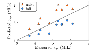
In the following, we compare the measured Hamiltonian parameters to those obtained using the LOM method applied to the physical layout of the devices. We focus on the most challenging parameter to obtain quantitative agreement for, .
We model the qubit cell as depicted in Fig. 1(b) by including; a short segment of charge control line, neighboring CPW structures, and all of the coupler structures attached to the qubit in the cell model. We extract the qubit cell Maxwell capacitance matrix using Ansys Q3D Extractor by using the layout geometry and a nominal substrate relative permittivity (Krupka et al., 2006) . We estimate the nominal Josephson junction intrinsic capacitance . The matrix is treated and reduced as described in Sec. I, after which we find a notably large capacitance to ground , in excess of , loading the readout coupling node . The effective CPW lengths are extracted from Eq. (17), where impedance and phase velocity , where is the speed of light, of the lines were found analytically from the line geometry (Simons, 2001). Finally, the qubit Josephson tunnel junction inductance is varied from its nominal values, inferred from room-temperature resistance measurements (Gloos et al., 2000), due to its unavoidable and inherent aging and cool-down variability, to obtain a qubit frequency agreement at the 1% level.
While some parameters of the model are known with exceedingly high precision, such as the geometry of the qubit device, we allow for small, reasonable variation in several parameters that are less well known. The variation in caused by the roughly 5% uncertainty inherent in these parameters, including and , is detailed in Table 1. Furthermore, for achieving the highest level of agreement, we detail in Table 1 the relative importance of including finer-order effects in the Hamiltonian model, such as the coupling of the qubit to the readout CPW first-harmonic mode. While this particular contribution has only a single-percent level effect on , including all direct CPW-CPW couplings originating from the direct capacitive links in the qubit cell, described in the Hamiltonian as terms of the form , significantly decreases the cross-Kerr by approximately 5%. In practice, since the qubit cell is only strongly coupled to a small handful of modes, we numerically diagonalize each individual system Hamiltonian first, constructing the composite Hamiltonian , using Eqs. (1) and (2) and diagonalizing the full system, from which we extract all final model parameters.
Accounting for these finer effects, we present the comparison between experimentally measured and LOM-predicted values of in Fig. 4. Across the 10 devices, we find that the agreement between theory and experiment is -10.5%. We compare this to a naive model, which disregards these finer effects and, chiefly, does not account for the large renormalization of the transmission line eigenmodes as detailed in Sec. III, illustrated in Fig. 3. Under these more conventional approximations, the average theory-experiment agreement is +19%. A chief component in the difference is the large magnitude of , which dresses down the CPW readout mode frequency from approximately 8.8 GHz to 7.0 GHz, a 25% renormalization effect.
In Table 1, we summarize the fluctuation in the agreement between simulated and measured from the modification of model features and parameters . For example, the table reports the effect of varying the location of the qubit cell partition and the length of neighboring CPWs included in the qubit cell model. This is found to have a nearly negligible effect. Determination of the consistently correct amount to include was not reached, though for the transmon layouts this paper considered, m proved to be sound. The separation of the device chips has a small effect when the gap is larger than the feature dimensions (Minev et al., 2016), though becomes significant when said gap is equivalent to or less than feature dimensions. Including the sample holder packaging in the model has a negligible effect for the dimensions of our device. It is not possible to achieve perfect experimental agreement by varying the model parameters within experimental tolerances. In fact, the model is fairly well constrained. We believe that better agreement requires a more complete model description of distributed effects. These can be captured by more computationally-expensive, but also more informationally-complete treatments, such as impedance (Nigg et al., 2012) or energy-participation ratio (EPR) quantization (Minev et al., 2020).
Conclusion.
We introduced the lumped-oscillator method (LOM) and studied its experimental performance on state-of-the-art superconducting quantum processors (Antonio D. et al., 2021). We found the LOM method to be practical, due to its systematic and modular analysis flow. It operates by partitioning the device in a two-fold manner—subsystems and simulation cells. Cells are small domains of the physical device layout, which can be independently analyzed using analytical results or numerical simulations. Breaking up the device layout into independent cells increases the computational modeling efficiency. Subsystems serve as small, familiar building blocks. Within the lumped approximation, the full Hamiltonian of the composite system is extracted with no approximations on the strength or nature of the inductive non-linear dipoles. Subsystem-subsystem couplings can be arbitrarily large. This was experimentally important to account for the data. We observed subsystem renormalizations on the order of 25% in the experiment due to dressings induced by the coupler structures and the subsystem embedding in the larger network. Overall, we found a two-times improvement in experimental agreement using the LOM method over one that makes weak coupling approximations and does not fully account for the non-perturbative dressing of the distributed modes.
With the increased complexity and demands driven by the rapid development of quantum hardware, we believe fast, accurate, and systematic techniques such as the LOM method presented here will be an essential ingredient in the development of current and future quantum technology. For this reason, we contribute the automation and implementation of this method to the community, as part of our open-source project Qiskit Metal | for quantum device design (Note, 1).
Acknowledgements.
We thank M. Malekakhlagh, F. Solgun, D.C. McKay, D. Wang, and R. Gutiérrez-Jáuregui for valuable discussions. We are grateful to all the early-access participants of Qiskit Metal and the Metal team for discussions and stress testing the open-source code. We thank G. Calusine and W. Oliver for providing the traveling-wave parametric amplifier used in this work. We acknowledge partial support for work on the simulations, and experimental bring-up and characterization of the devices from the Intelligence Advanced Research Projects Activity (IARPA) under Contract No. W911NF-16-1-0114.
Author contributions.
Z.K.M developed the theory and software, and wrote the manuscript. Z.K.M. conceived of the project based on work by J.M.G., who oversaw the work. Z.K.M. and T.G.M. simulated and analyzed the devices. M.T. and A.C. performed the experimental bring-up and characterization of the devices and worked with Z.K.M on the analysis of the experimental data. All authors discussed the results and contributed to the manuscript.
Code availability.
The source code for Qiskit Metal | for quantum device design and for the LOM method implementation is open-sourced and can be found at github.com/qiskit/qiskit-metal.
Appendix A Maxwell capacitance matrix
The effective capacitances of a cell can be extracted from its physical layout. A simulation incorporating the cell geometry, materials, and electromagnetic boundary conditions can yield its Maxwell capacitance matrix . For a cell with nodes (nets), is an square, full-rank matrix. Its off-diagonal entries are the negative of the capacitance between nodes and , where . Its -th diagonal is the self-capacitance of the -th node to infinity plus the value of all coupled capacitances; i.e., the -th row and -th column element of is
| (A1) |
For example, the Maxwell matrix for the set of nodes has the form
where we introduce the shorthand and, for simplicity, we omit the lower-triangular block of the symmetric matrix. The sum of the -th row and identically the -th column of is the self-capacitance (to infinity) of the -th node. An abstract conductor at infinity serves as the effective datum of the schematic corresponding to the Maxwell matrix. The matrix is expressed in the basis of node fluxes referenced to that infinity conductor, assumed at zero potential; note, .
By selecting as the physical ground node and datum of the circuit, we set its respective flux to zero. We need to thus eliminate as a degree of freedom and reduce the flux basis to an -length column vector of node-to-datum fluxes ; note, . We perform the basis reduction with the nearly-trivial linear transformation , where is the column vector of all zeros with length and is the identity matrix of dimension . In the reduced basis , the reduced capacitance matrix of the cell is
Due to the simple form of , this is equivalent to simply dropping the first row and column of ; i.e.,
where the set of non-datum nodes of the cell is .
References
- Devoret and Schoelkopf (2013) M. H. Devoret and R. J. Schoelkopf, Science 339, 1169 (2013).
- Gambetta et al. (2017) J. M. Gambetta, J. M. Chow, and M. Steffen, npj Quantum Information 3, 2 (2017).
- Krantz et al. (2019) P. Krantz, M. Kjaergaard, F. Yan, T. P. Orlando, S. Gustavsson, and W. D. Oliver, Applied Physics Reviews 6, 021318 (2019).
- Kjaergaard et al. (2020) M. Kjaergaard, M. E. Schwartz, J. Braumüller, P. Krantz, J. I. Wang, S. Gustavsson, and W. D. Oliver, “Superconducting Qubits: Current State of Play,” (2020), arXiv:1905.13641 .
- Blais et al. (2020) A. Blais, A. L. Grimsmo, S. M. Girvin, and A. Wallraff, (2020), arXiv:2005.12667 .
- Nigg et al. (2012) S. E. Nigg, H. Paik, B. Vlastakis, G. Kirchmair, S. Shankar, L. Frunzio, M. H. Devoret, R. J. Schoelkopf, and S. M. Girvin, Physical Review Letters 108, 240502 (2012).
- Bourassa et al. (2012) J. Bourassa, F. Beaudoin, J. M. Gambetta, and A. Blais, Physical Review A 86, 013814 (2012), arXiv:arXiv:1204.2237v2 .
- Solgun et al. (2014) F. Solgun, D. W. Abraham, and D. P. DiVincenzo, Physical Review B 90, 134504 (2014).
- Solgun and DiVincenzo (2015) F. Solgun and D. P. DiVincenzo, Annals of Physics 361, 605 (2015), arXiv:1505.04116 .
- Smith et al. (2016) W. C. Smith, A. Kou, U. Vool, I. M. Pop, L. Frunzio, R. J. Schoelkopf, and M. H. Devoret, Physical Review B 94, 144507 (2016), arXiv:1602.01793 .
- Malekakhlagh and Türeci (2016) M. Malekakhlagh and H. E. Türeci, Physical Review A 93, 012120 (2016), arXiv:1506.02773 .
- Gely et al. (2017) M. F. Gely, A. Parra-Rodriguez, D. Bothner, Y. M. Blanter, S. J. Bosman, E. Solano, and G. A. Steele, Physical Review B 95, 245115 (2017).
- Malekakhlagh et al. (2017) M. Malekakhlagh, A. Petrescu, and H. E. Türeci, Physical Review Letters 119, 073601 (2017).
- Pechal and Safavi-Naeini (2017) M. Pechal and A. H. Safavi-Naeini, Physical Review A 96, 042305 (2017), arXiv:1706.05368 .
- Minev et al. (2018) Z. K. Minev, Z. Leghtas, S. O. Mudhada, P. Reinhold, A. Diringer, and M. H. Devoret, “pyEPR: The energy-participation-ratio (EPR) open-source framework for quantum device design,” (2018).
- Parra-Rodriguez et al. (2019) A. Parra-Rodriguez, I. L. Egusquiza, D. P. DiVincenzo, and E. Solano, Physical Review B 99, 014514 (2019), arXiv:1810.08471 .
- Parra-Rodriguez et al. (2018) A. Parra-Rodriguez, E. Rico, E. Solano, and I. L. Egusquiza, Quantum Science and Technology 3, 024012 (2018), arXiv:1711.08817 .
- Ansari (2019) M. H. Ansari, Physical Review B 100, 024509 (2019), arXiv:1807.00792 .
- Krupko et al. (2018) Y. Krupko, V. D. Nguyen, T. Weißl, É. Dumur, J. Puertas, R. Dassonneville, C. Naud, F. W. J. Hekking, D. M. Basko, O. Buisson, N. Roch, and W. Hasch-Guichard, Physical Review B 98, 094516 (2018).
- Malekakhlagh et al. (2020a) M. Malekakhlagh, A. Petrescu, and H. E. Türeci, Physical Review B 101, 134509 (2020a), arXiv:1809.04667 .
- Solgun et al. (2019) F. Solgun, D. P. DiVincenzo, and J. M. Gambetta, IEEE Transactions on Microwave Theory and Techniques 67, 928 (2019), arXiv:1712.08154 .
- Petrescu et al. (2019) A. Petrescu, M. Malekakhlagh, and H. E. Türeci, (2019), arXiv:1908.01240 .
- You et al. (2019) X. You, J. A. Sauls, and J. Koch, Physical Review B 99, 174512 (2019), arXiv:1902.04734 .
- Di Paolo et al. (2019) A. Di Paolo, T. E. Baker, A. Foley, D. Sénéchal, and A. Blais, (2019), arXiv:1912.01018 .
- Gely and Steele (2020) M. F. Gely and G. A. Steele, New Journal of Physics 22, 013025 (2020).
- Ding et al. (2020) D. Ding, H. S. Ku, Y. Shi, and H. H. Zhao, “Free mode removal and mode decoupling for simulating general superconducting quantum circuits,” (2020), arXiv:2011.10564 .
- Kerman (2020) A. J. Kerman, (2020), arXiv:2010.14929 .
- Minev et al. (2020) Z. K. Minev, Z. Leghtas, S. O. Mundhada, L. Christakis, I. M. Pop, and M. H. Devoret, arXiv (2020), arXiv:2010.00620 .
- Kyaw et al. (2020) T. H. Kyaw, T. Menke, S. Sim, N. P. D. Sawaya, W. D. Oliver, G. G. Guerreschi, and A. Aspuru-Guzik, (2020), arXiv:2006.03070 .
- Malekakhlagh et al. (2020b) M. Malekakhlagh, E. Magesan, and D. C. McKay, (2020b), arXiv:2005.00133 .
- Menke et al. (2021) T. Menke, F. Häse, S. Gustavsson, A. J. Kerman, W. D. Oliver, and A. Aspuru-Guzik, npj Quantum Information 7, 49 (2021), arXiv:1912.03322 .
- Wallraff et al. (2004) A. Wallraff, D. I. Schuster, A. Blais, L. Frunzio, R.-S. Huang, J. Majer, S. Kumar, S. M. Girvin, and R. J. Schoelkopf, Nature 431, 162 (2004), arXiv:0407325 [cond-mat] .
- Paik et al. (2011) H. Paik, D. I. Schuster, L. S. Bishop, G. Kirchmair, G. Catelani, A. P. Sears, B. R. Johnson, M. J. Reagor, L. Frunzio, L. I. Glazman, S. M. Girvin, M. H. Devoret, and R. J. Schoelkopf, Physical Review Letters 107, 240501 (2011), arXiv:1105.4652 .
- Barends et al. (2013) R. Barends, J. Kelly, A. Megrant, D. Sank, E. Jeffrey, Y. Chen, Y. Yin, B. Chiaro, J. Mutus, C. Neill, P. O’Malley, P. Roushan, J. Wenner, T. C. White, A. N. Cleland, and J. M. Martinis, Physical Review Letters 111, 080502 (2013), arXiv:1304.2322 .
- Minev et al. (2013) Z. Minev, I. M. Pop, and M. H. Devoret, Applied Physics Letters 103, 142604 (2013), arXiv:arXiv:1308.1743v1 .
- Yan et al. (2016) F. Yan, S. Gustavsson, A. Kamal, J. Birenbaum, A. P. Sears, D. Hover, T. J. Gudmundsen, D. Rosenberg, G. Samach, S. Weber, J. L. Yoder, T. P. Orlando, J. Clarke, A. J. Kerman, and W. D. Oliver, Nature Communications 7, 12964 (2016).
- Brecht et al. (2016) T. Brecht, W. Pfaff, C. Wang, Y. Chu, L. Frunzio, M. H. Devoret, and R. J. Schoelkopf, npj Quantum Information 2, 16002 (2016), arXiv:1509.01127 .
- Rosenberg et al. (2017) D. Rosenberg, D. Kim, R. Das, D. Yost, S. Gustavsson, D. Hover, P. Krantz, A. Melville, L. Racz, G. O. Samach, S. J. Weber, F. Yan, J. L. Yoder, A. J. Kerman, and W. D. Oliver, npj Quantum Information 3, 42 (2017), arXiv:1706.04116 .
- Versluis et al. (2017) R. Versluis, S. Poletto, N. Khammassi, B. Tarasinski, N. Haider, D. J. Michalak, A. Bruno, K. Bertels, and L. DiCarlo, Physical Review Applied 8, 034021 (2017).
- Naik et al. (2017) R. K. Naik, N. Leung, S. Chakram, P. Groszkowski, Y. Lu, N. Earnest, D. C. McKay, J. Koch, and D. I. Schuster, Nature Communications 8, 1904 (2017).
- Charles James Neill (2017) Charles James Neill, Thesis, Tech. Rep. (2017).
- Yan et al. (2018) F. Yan, P. Krantz, Y. Sung, M. Kjaergaard, D. L. Campbell, T. P. Orlando, S. Gustavsson, and W. D. Oliver, Physical Review Applied 10, 054062 (2018), arXiv:1803.09813 .
- Minev et al. (2019) Z. K. Minev, S. O. Mundhada, S. Shankar, P. Reinhold, R. Gutiérrez-Jáuregui, R. J. Schoelkopf, M. Mirrahimi, H. J. Carmichael, and M. H. Devoret, Nature 570, 200 (2019), arXiv:1803.00545 .
- Antonio D. et al. (2021) Antonio D., M. Takita, K. Inoue, S. Lekuch, Z. K. Minev, J. M. Chow, and J. M. Gambetta, (2021), arXiv:2102.01682 .
- Yurke and Denker (1984) B. Yurke and J. S. Denker, Physical Review A 29, 1419 (1984).
- Devoret (1995) M. H. Devoret, in Quantum Fluctuations, Les Houches, Sess. LXIII (1995).
- Burkard et al. (2004) G. Burkard, R. H. Koch, and D. P. DiVincenzo, Physical Review B 69, 064503 (2004).
- Koch et al. (2007) J. Koch, T. M. Yu, J. Gambetta, A. A. Houck, D. I. Schuster, J. Majer, A. Blais, M. H. Devoret, S. M. Girvin, and R. J. Schoelkopf, Physical Review A 76, 42319 (2007).
- Note (1) For an early version of the open-source code (Minev et al., 2021) developed by the authors of this manuscript, see qiskit.org/metal. The Qiskit Metal project builds on github.com/zlatko-minev/pyEPR.
- Zimmerman and Silver (1966) J. E. Zimmerman and A. H. Silver, Physical Review 141, 367 (1966).
- Clarke and Braginski (2004) J. Clarke and A. I. Braginski, eds., The SQUID Handbook (Wiley-VCH Verlag GmbH & Co. KGaA, Weinheim, FRG, 2004).
- Frattini et al. (2018) N. E. Frattini, V. V. Sivak, A. Lingenfelter, S. Shankar, and M. H. Devoret, Physical Review Applied (2018), 10.1103/PhysRevApplied.10.054020, arXiv:1806.06093 .
- Minev (2019) Z. K. Minev, Ph.D. thesis, Yale University (2019), arXiv:1902.10355 .
- Gloos et al. (2000) K. Gloos, R. S. Poikolainen, and J. P. Pekola, Applied Physics Letters 77, 2915 (2000).
- Wolff (2006) I. Wolff, Coplanar Microwave Integrated Circuits (John Wiley & Sons, Inc., Hoboken, NJ, USA, 2006).
- Dirac (1982) P. A. M. Dirac, Principles of Quantum Mechanics (Oxford University Press, 1982).
- Note (2) This is the form employed in a recent package entitled scqubits; see also Ref. \rev@citealpnumKerman2020.
- Minev et al. (2021) Z. K. Minev, T. G. McConkey, J. Drysdal, P. Shah, D. Wang, M. Facchini, G. Harper, J. Blair, H. Zhang, N. Lanzillo, S. Mukesh, W. Shanks, C. Warren, and J. M. Gambetta, “Qiskit Metal: An Open-Source Framework for Quantum Device Design & Analysis,” (2021).
- Zangwill (2012) A. Zangwill, Modern Electrodynamics (Cambridge University Press, 2012).
- Blais et al. (2004) A. Blais, R.-S. Huang, A. Wallraff, S. M. Girvin, and R. J. Schoelkopf, Physical Review A 69, 062320 (2004), arXiv:0402216 [cond-mat] .
- Gambetta et al. (2006) J. Gambetta, A. Blais, D. I. Schuster, A. Wallraff, L. Frunzio, J. Majer, M. H. Devoret, S. M. Girvin, and R. J. Schoelkopf, Physical Review A - Atomic, Molecular, and Optical Physics (2006), 10.1103/PhysRevA.74.042318, arXiv:0602322 [cond-mat] .
- Gambetta et al. (2008) J. Gambetta, A. Blais, M. Boissonneault, A. A. Houck, D. I. Schuster, and S. M. Girvin, Physical Review A 77, 012112 (2008).
- Krupka et al. (2006) J. Krupka, J. Breeze, A. Centeno, N. Alford, T. Claussen, and L. Jensen, IEEE Transactions on Microwave Theory and Techniques 54, 3995 (2006).
- Simons (2001) R. N. Simons, Coplanar Waveguide Circuits, Components, and Systems (2001).
- Minev et al. (2016) Z. Minev, K. Serniak, I. M. Pop, Z. Leghtas, K. Sliwa, M. Hatridge, L. Frunzio, R. J. Schoelkopf, and M. H. Devoret, Physical Review Applied 5, 044021 (2016), arXiv:1509.01619 .