Plasmonically enhanced spectrally selective narrowband MWIR and LWIR light detection based on hybrid nanopatterned graphene and phase changing vanadium oxide heterostructure operating close to room temperature
Abstract
We present the model of an ultrasensitive mid-infrared (mid-IR) photodetector operating in the mid-wavelength infrared (MWIR) and long-wavelength infrared (LWIR) domains consisting of a hybrid heterostructure made of nanopatterned graphene (NPG) and vanadium dioxide (VO2) which exhibits a large responsivity of V/W, a detectivity exceeding J, and a sensitivity in terms of noise-equivalent power fW/ close to room temperature by taking advantage of the phase change of a thin VO2 film. Our proposed photodetector can reach an absorption of nearly 100% in monolayer graphene due to localized surface plasmons (LSPs) around the patterned circular holes. The geometry of the nanopattern and an electrostatic gate potential can be used to tune the absorption peak in the mid-IR regime between 3 and 12 m. After the photon absorption by the NPG sheet and the resulting phase change of VO2 from insulating to metallic phase the applied bias voltage triggers a current through the VO2 sheet, which can be detected electronically in about 1 ms, shorter than the detection times of current VO2 bolometers. Our envisioned mid-IR photodetector reaches detectivities of cryogenically cooled HgCdTe photodetectors and sensitivities larger than VO2 microbolometers while operating close to room temperature.
KEYWORDS: Localized surface plasmons, graphene, absorbance, vanadium dioxide, photodetection, bolometer.
Due to the low photon energy of IR radiation cryogenic cooling is required for highly sensitive photodetection based on low band gap materials like mercury-cadmium-telluride (HgCdTe). Various kinds of microbolometers primarily based on vanadium oxide (VOx) offer uncooled detection of IR radiation. However, microbolometers suffer from low sensitivity, slow response and tedious multi-step complex lithographic processes Rogalski (2002). Photodetection based on the bolometric effect takes advantage of the dependence of the resistivity on the temperature to detect incident light, typically in the infrared regime. Vanadium oxide (VO2) has become one of the standard materials for building microbolometers with broadband mid-IR photodetection because it features a reversible insulator-to-metal phase transition (IMT) when heated above the phase transition temperature , which is slightly above and close to room temperature Rogalski (2011). Bulk VO2 undergoes a phase transition from an insulating state with monoclinic crystal structure below 68∘C to a metallic state with rutile crystal structure above C (=341 K) Goodenou (1971); Morin (1959); Chandra et al. (2018). This phase transition is fully reversible with a hysteresis loop, occurs on a subpicosecond timescale Appavoo and Haglund (2011); Dicken et al. (2009), and can be initiated either thermally, electrically Stefanovich et al. (2000), or optically Cavalleri et al. (2001). While for bulk VO2 optically induced IMT can only be achieved by pumping above the band gap of meV of bulk VO2, it is possible to induce IMT in thin films at energies of 200 meV and above (corresponding to wavelengths of m and below) due to electronic defects inside the band gap Rini et al. (2008), which is the reason why VO2 thin films can be used for IR detection in a wide IR range, in particular in the 3-5 m range. Interestingly, when VO2 is in the form of a thin film, its transition temperature depends strongly on the thickness d of the film, i.e. decreases from 65∘C (=338 K) for nm down to 52∘C (=325 K) for nm Xu et al. (2005). While IR radiation with wavelengths above about m cannot detect the change in thickness of around 20 nm, it certainly distinguishes between the insulating and the metallic phase of VO2. All these properties make VO2 the ideal material for developing mid-IR photodetectors based on the IMT effect.
However, photodetection of mid-IR light with wavelength above about 6 m is inefficient with VO2 bulk or thin films because of the relatively weak interaction between the incident photons and the optical phonons in VO2. This interaction is so weak that the IMT cannot be achieved. That is why in the wavelength regime of 8 to 12 m the photodetection is based purely on the bolometric effect in the semiconducting phase of VO2 Barker et al. (1966); Chen et al. (2001). Here, by adding a single layer of nanopatterned graphene (NPG) on top of a layer of VO2, we present the model of a photodetector that not only greatly enhances the absorption of mid-IR light energy in the longer wavelength regime from m and exceeding 12 m but also narrows the absorption bandwidth to 0.1 m within the mid-IR range of 3 to 12 m, thereby enabling plasmonically enhanced spectrally selective absorption of mid-IR light for the IMT effect in a heterostructure made of NPG and VO2.
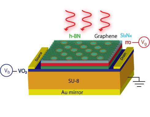
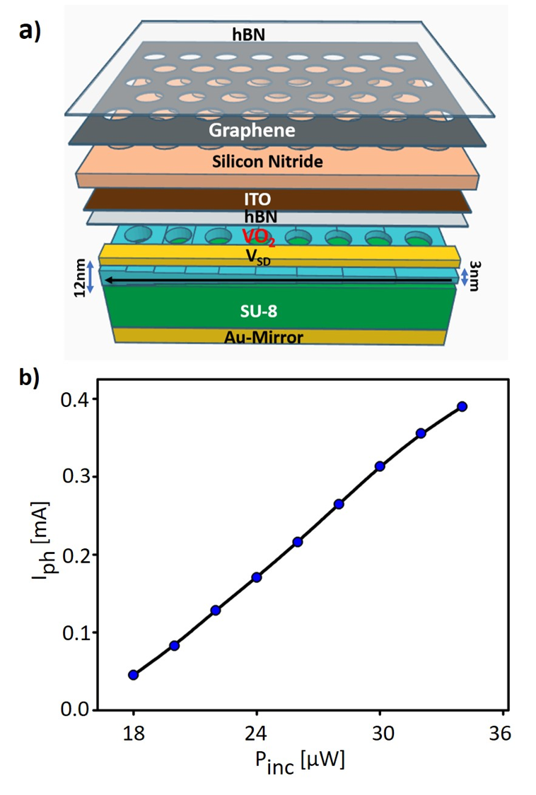
Building upon the knowledge we acquired for developing spectrally selective photodetectors made of NPG that detect mid-IR light by means of the photothermoelectric effect Safaei et al. (2017, 2019a, 2019b) and the knowledge we acquired for developing thermal emitters based on NPG Shabbir and Leuenberger (2020), we develop here the model of a mid-IR microbolometer that consists of an hexagonal boron nitride (h-BN) coated NPG, silicon nitride (Si3N4), indium tin oxide (ITO), VO2, polymer, and gold (Au) mirror, as shown in Fig. 1. The main working principle of our envisioned mid-IR photodetector can be summarized as follows. After mid-IR photons get absorbed by the NPG sheet at a wavelength that matches the localized surface plasmon (LSP) resonance, the NPG’s temperature increases and transfers the heat through the Si3N4 and ITO layers to the VO2 layer. By patterning not only the graphene sheet but also the Si3N4 and ITO layers we maximize the heat transfer to the VO2 layer. Once the VO2 layer’s temperature increases above the phase transition temperature , the VO2 layer undergoes a transition from insulating to metallic phase. The patterning of the VO2 layer decreases its volume, thereby decreasing the heat required to drive the VO2 layer over , which in turn increases the sensitivity (NEP) of our proposed NPG-VO2 photodetector. During this whole time a bias voltage is applied to the VO2 layer, which upon phase transition triggers a current through the VO2 layer, which can be detected electronically in about 1 ms, shorter than the detection time of typical VO2 bolometers Chen et al. (2001).
For the electronic response of the graphene sheet and the VO2 layer to the incident mid-IR photons, we need to consider the intraband conductivity of graphene and the dielectric function of VO2 in the insulating and metallic regimes. Using the linear dispersion relation, the intraband optical conductivity of graphene is Safaei et al. (2017); Paudel et al. (2017)
| (1) |
which in the case of is reduced to
| (2) |
where is determined by impurity scattering and electron-phonon interaction . Using the mobility of the NPG sheet, it can be presented in the form , where m/s is the Fermi velocity in graphene. is the bulk graphene plasma frequency.
The dielectric function of VO2 can be approximated by means of a constant for the insulating phase Jepsen et al. (2006),
| (3) |
and by means of the Drude formula for the metallic phase,
| (4) |
where is the plasma frequency of VO2, is the scattering rate in VO2, with cm2/Vs being the mobility in VO2, cm-3 the free-carrier concentration in VO2, and the effective mass of the charge carriers in VO2. is the free electron mass. is the fraction of the original velocity of the electron after scattering.
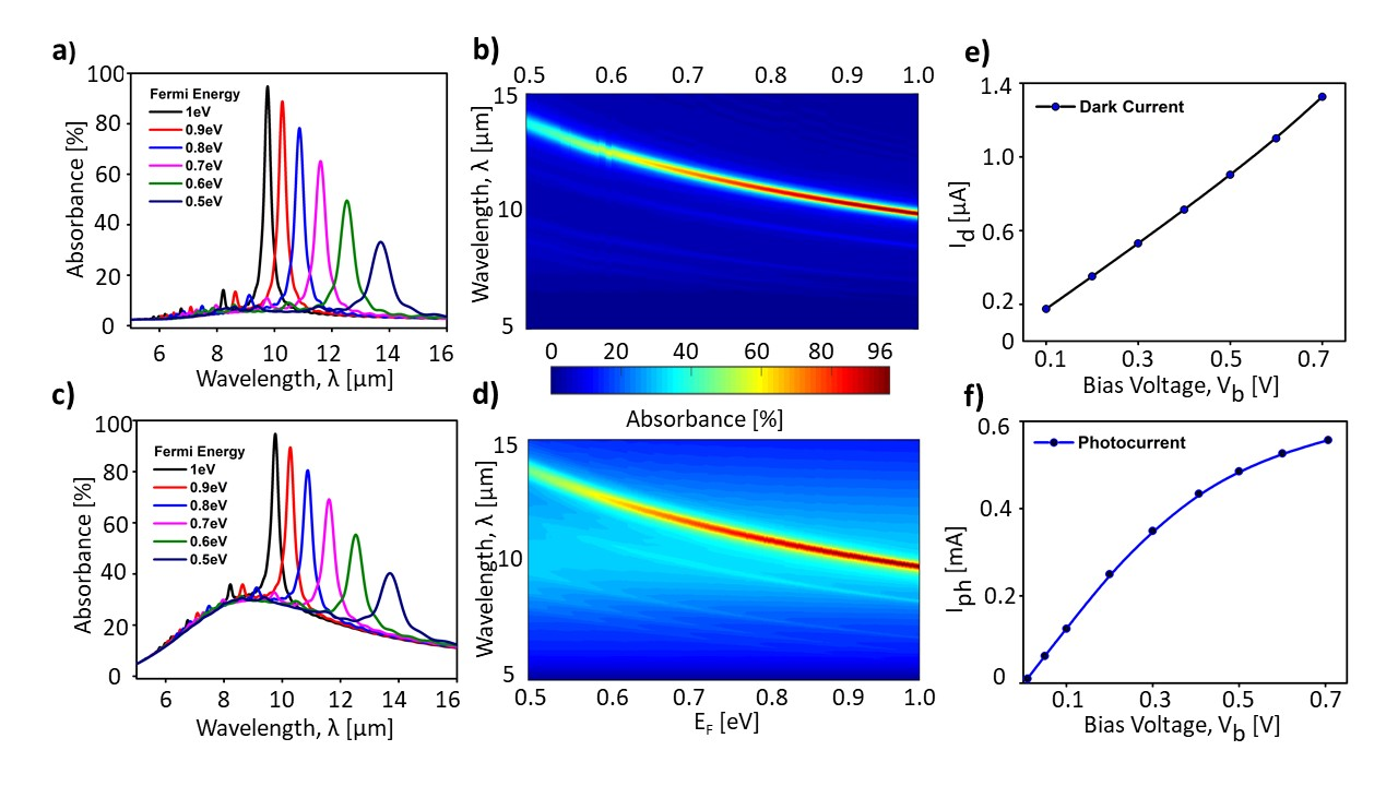
We used the finite-difference time domain method (FDTD) to calculate the absorbance of the hybrid NPG-VO2 photodetector as shown in Fig. 2 (a) when VO2 is in the insulating phase and in Fig. 2 (c) when VO2 is in the metallic phase. The resonance peaks due to the absorption of mid-IR light by localized surface plasmons (LSPs) in NPG are clearly visible and similar to the ones found in Refs. Safaei et al. (2017, 2019a, 2019b); Shabbir and Leuenberger (2020). The main difference is that the VO2 layer exhibits very low absorbance (around 6%) of mid-IR light in the insulating phase but a larger broadband absorption in the metallic phase. The thicker the metallic VO2 layer is, the stronger is the absorption of mid-IR light. We chose a VO2 layer thickness of 3 nm for two important reasons: Firstly, a thinner VO2 layer results in weaker absorption and thus makes it easier for the photodetector to cool down after the incident mid-IR radiation is turned off. Secondly, the thinner VO2 layer has a lower phase transition temperature of C (=325 K) and thus requires less external heating for keeping the photodetector at an optimum operating temperature (see below).
The absorbance resonance peak as a function of wavelength can be tuned by means of the Fermi energy of NPG, as shown in Fig. 2 (b) when VO2 is in the insulating phase and in Fig. 2 (d) when VO2 is in the metallic phase. Thus, the gate voltage allows the operating wavelength of the VO2-NPG photodetector to be tuned in addition to the size and period of the nanopattern in graphene.
For modeling the operation of the proposed NPG-VO2 mid-IR photodetector, we used COMSOL and the following theory for the thermoelectric properties of VO2 close to the phase transition temperature . The VO2 layer is operated around the IMT phase transition temperature . The performance of the bolometric detection can be analyzed by means of the heat equation and a hysteresis model de Almeida et al. (2004). The heat equation reads
| (5) |
where is the heat capacity, is the absorbance, is the power of the incident radiation, is the time-independent bias current, is the temperature-dependent resistance, is the thermal conductivity of the heat sink, and is the time-independent temperature of the heat sink. The hysteretic behavior of for VO2 layer can be calculated by
| (6) |
where the semiconductor volume fraction is given by
| (7) |
where is the width of the hysteresis, is a function of at , is an arbitrary monotonically decreasing function, and . The proximity temperature is given by
| (8) |
Eqs. (5)-(8) provide a simple method to describe the hysteretic behavior of the plasmonically driven bolometric photodetector. The incident power is then given by the energy pumped into the plasmonic nanostructure.
Using this thermoelectric theory and combining it with our FDTD results, we developed a photothermoelectric theory of the NPG-VO2 heterostructure. We present the current as a function of applied bias voltage (I-V characteristics) for insulating VO2 in Fig 2 (e). and for metallic VO2 in Fig. 2 (f). Note that the current flows only through VO2, not through NPG. NPG is used only as a photothermoelectric heating element. When the incident mid-IR light is off, a very weak dark current on the scale of A is flowing when a bias voltage is applied on the order of 0.1 to 1.0 V. In stark contrast, when the incident mid-IR light is on, a much larger light current on the scale of mA is flowing with the same applied bias voltage . This effect is due to the phase transition of VO2 between insulating and metallic phases. We take advantage of this effect to develop the model of an ultrasensitive photodetector based on the NPG-VO2 heterostructure.
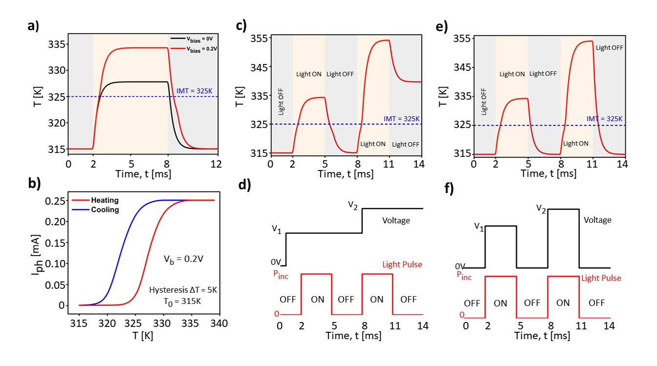
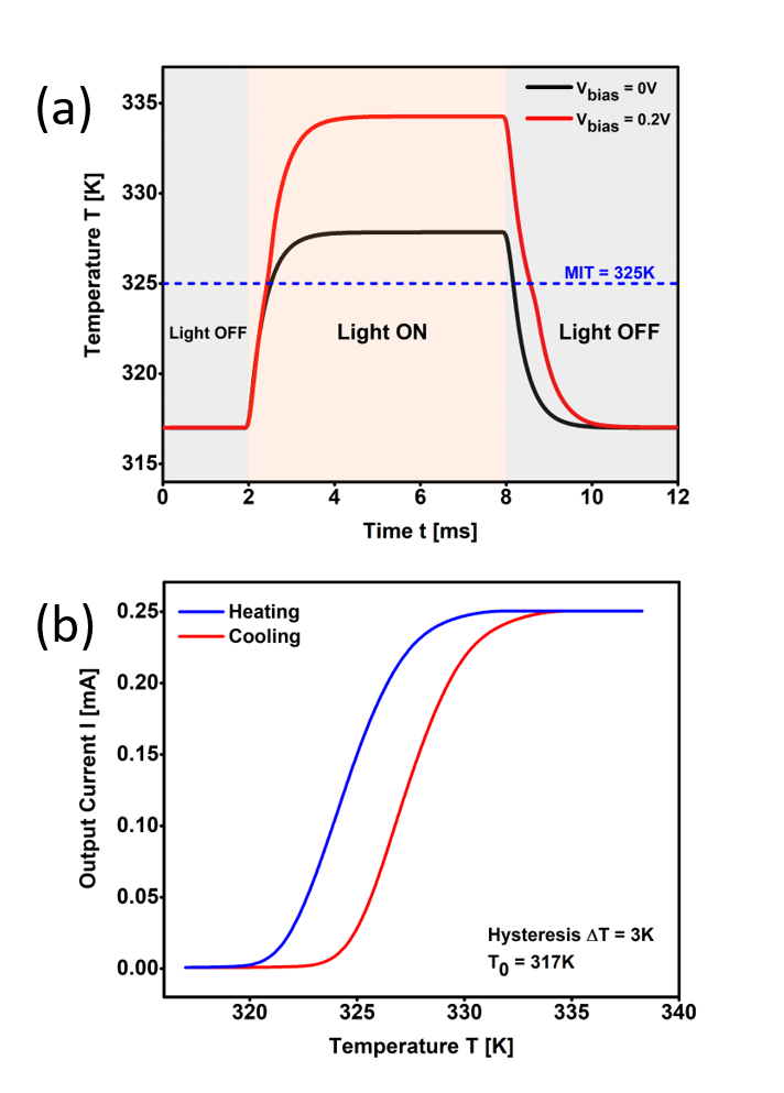
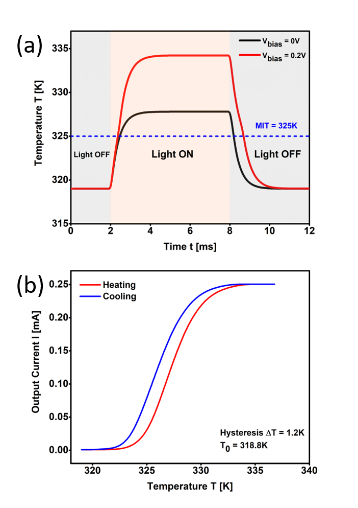
After modeling the heating and cooling of the NPG-VO2 heterostructure as a function of time, we identified the optimum photodetection process. The resulting temperature of the VO2 layer as a function of time and the photocurrent through the VO2 layer as a function of temperature for a constant applied bias voltage V are shown in Fig. 3 (a) and (b). We used the theoretical models and experimental values of conductivity, thermal conductivity, and heat capacity of VO2 given in Refs. Qazilbash et al. (2009); Zhong et al. (2011); Samanta et al. (2015); Ordonez-Miranda et al. (2018). Our results reveal that the NPG-VO2 photodetector has a response time on a time scale of the order of 1 ms, shorter than current microbolometers based on VO2 alone Chen et al. (2001).
The amount of Joule heating can be seen in Fig. 3(a) as the difference in temperature between the cases V and V. When the applied bias voltage is kept constant and is too large, the Joule heating prevents the photodetector from coolling down, as shown in Fig. 3 (c) and (d). Such a behavior is problematic. In order to overcome this problem, one can apply a pulsed bias voltage , which ensures the cooling of the photodetector below the phase transition temperature , as shown in Fig. 3 (e) and (f).
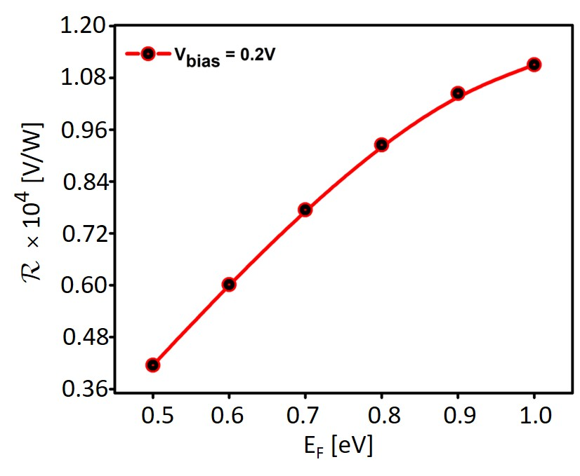
The responsivity of the NPG-VO2 photodetector can be calculated by means of the formula Safaei et al. (2019b)
| (9) |
where is the resistance of VO2 in the metallic phase, is the light current when the incident light is on, is the dark current when the incident light is off, and is the power of the incident light. The responsivity as a function of Fermi energy of NPG is shown in Fig. 4.
The sensitivity of the NPG-VO2 photodetector is determined by the noise-equivalent power NEP, being an important figure of merit for the performance of a photodetector. The NEP of a photodetector provides a measure for the minimum detectable power per 1 Hz of bandwidth. The formula for NEP reads Safaei et al. (2019b)
| (10) |
where
| (11) |
is the root-mean-square of the total noise voltage, which consists of the sum over all possible noise voltages, such as the thermal Johnson-Nyquist noise , due to thermal motion of the charge carriers and independent of the bias voltage , the shot noise , due to the discrete nature of uncorrelated charge carriers, and the noise , also called flicker noise, due to random resistance fluctuations. The Johnson noise is given by Guo et al. (2020)
| (12) |
where is the Botzmann constant, is the temperature, and is the resistance. The shot noise is given by Guo et al. (2020)
| (13) |
where is the elementary charge and is the dark current. Since the dark current is very low and the NPG-VO2 photodetector operates close to room temperature, the shot noise is much smaller than the Johnson noise. Therefore, we can safely neglect the shot noise. At a modulation frequency of of around 1 kHz we can also neglect the noise. Using the NEP, we can calculate the detectivity of the NPG-VO2 photodetector by means of the formula Safaei et al. (2019b)
| (14) |
where is the area of the photodetector. The results of these figures of merit are shown in Table 1. By increasing the substrate temperature , it is possible to decrease the hysteresis temperature difference , which in turn results in an enhanced sensitivity NEP and a larger detectivity . The details of these additional results are shown in the supplementary material.
| [K] | [W] | [K] | NEP [fW/] | [Jones] | |
|---|---|---|---|---|---|
| 5.0 | 18.0 | 315.0 | 1.1 | 347 | 0.50 |
| 3.0 | 14.0 | 317.0 | 1.4 | 273 | 0.64 |
| 1.2 | 10.6 | 318.8 | 1.9 | 203 | 0.85 |
Table 1 shows that the detectivity of the NPG-VO2 photodetector operating close to room temperature is close to of cryogenically cooled HgCdTe photodetectors. The NPG-VO2 photodetector reaches a sensitivity close to VO2 microbolometers while exhibiting a shorter detection time of around 1 ms and being able to detect photons also in the LWIR regime, which is impossible for VO2 microbolometers.
Since we want to realize a linear dependence of the photocurrent as a function of input power of the mid-IR light, we add a gradient in the thickness of the VO2 layer as shown in Fig. 5 (a), i.e. the VO2 layer thickness is varied from 3 nm to 12 nm. The resulting linear photocurrent as a function of input power is shown in Fig. 5 (b). Indeed, the photocurrent is now linear as a function of the input power , which provides an optimized mapping of onto for maximum dynamic range.
In conclusion, we present the model of an ultrasensitive mid-infrared (mid-IR) photodetector based on a heterostucture made of NPG and VO2, thereby extending the responsivity of a VO2 microbolometer to the LWIR domain. Moreover, this hybrid NPG-VO2 photodetector has a narrowband absorption in the MWIR and LWIR that can be tuned by means of a gate voltage. Our results show that the NPG-VO2 photodetector can reach a large responsivity V/W, a detectivity Jones, and a sensitivity in terms of NEP fW/ close to room temperature by taking advantage of the phase change of a thin VO2 layer. The NPG sheet achieves an absorption of nearly 100% due to localized surface plasmons (LSPs) around the patterned circular holes in a hexagonal lattice symmetry. The electrostatic gate potential can be used to tune the wavelength peak in the MWIR and LWIR regimes between 3 and 12 microns, thereby overcoming the intrinsic upper limit of 6 microns for microbolometers based on VO2. Our COMSOL simulations show that the NPG-VO2 photodetector is able to operate on a time scale of 1 ms, much shorter than the response times of current microbolometers based on VO2 alone. Our proposed mid-IR photodetector reaches detectivities of cryogenically cooled HgCdTe photodetectors and sensitivities close to and field of view similar to VO2 microbolometers while operating close to room temperature.
Acknowledgements.
We acknowledge support from NSF CISE-1514089.I Supplementary Information
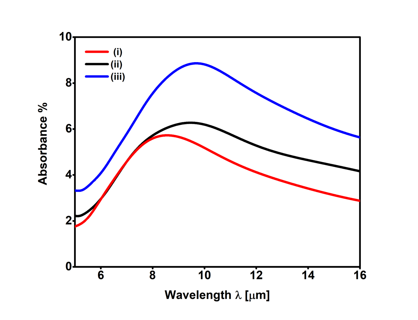
In order to show that NPG is absolutely required to achieve mid-IR photodetection in the wavelength range of m to 12 m as presented in this paper, we also calculated the absorbance and photocurrent for the cases (i) when graphene, Si3N4, and ITO are absent, (ii) when graphene is absent, and (iii) when graphene is not patterned. These results are compared with (iv) results for the NPG-VO2 photodetector shown in Fig. 1. All these results are shown in Table 2 in the case of V, base temperature K, incident radiation power W, wavelength m, and VO2 thickness of 3 nm.
| Geometry | [K] | [mA] | [mA] | [mA] |
|---|---|---|---|---|
| (i) | 316.8 | 0.35 | 0.369 | 0.019 |
| (ii) | 317.4 | 0.35 | 0.376 | 0.026 |
| (iii) | 317.7 | 0.35 | 0.381 | 0.031 |
| (iv) | 334.3 | 0.35 | 0.25 | 0.25 |
It can be seen from Table 2 that the cases (i) to (iii) achieve only a small photocurrent, in stark contrast to case (iv) that takes advantage of NPG. The reason for this large difference is the low absorbance of the structures (i) to (iii), as shown in Fig. 7.
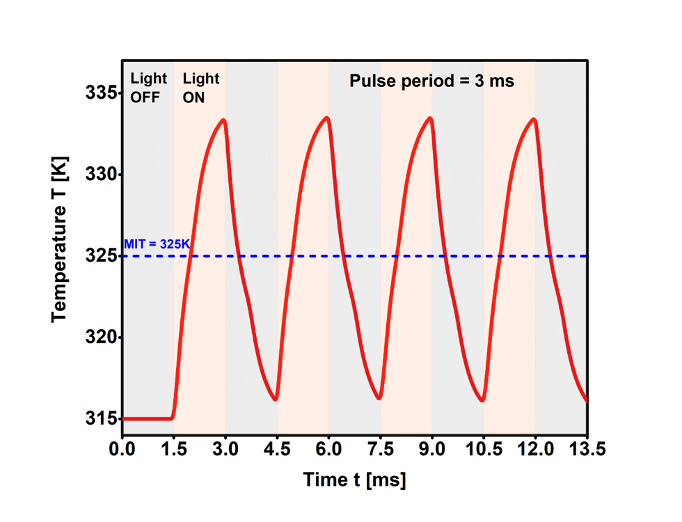
In order to study the response of the NPG-VO2 photodetector on a train of incident light pulses, we calculate the temperature as a function of time with pulse period ms. The result is shown in Fig. 6. Thus, the response time of the NPG-VO2 photodetector is of the order of 1 ms.
If the hysteresis curve of the photocurrent as a function of temperature can be made narrower with respect to the temperature Xu et al. (2012), then it is possible to increase the base temperature of the substrate . In that case, it is possible to reduce the required temperature difference for triggering the phase transition, which in turn allows us to also decrease the bias voltage , thereby reducing the generated Joule heating power inside metallic VO2. The temperature of VO2 as a function of time and the resulting photocurrent as a function of temperature for K and K is shown in Fig. 8, and for K and K is shown in Fig. 9.
References
- Rogalski (2002) A. Rogalski, Infrared Physics & Technology 43, 187 (2002).
- Rogalski (2011) A. Rogalski, Infrared Physics & Technology 54, 136 (2011).
- Goodenou (1971) J. Goodenou, Journal of Solid State Chemistry 3, 490 (1971).
- Morin (1959) F. J. Morin, Physical Review Letters 3, 34 (1959).
- Chandra et al. (2018) S. Chandra, D. Franklin, J. Cozart, A. Safaei, and D. Chanda, ACS Photonics 5, 4513 (2018).
- Appavoo and Haglund (2011) K. Appavoo and J. Haglund, Richard F., Nano Letters 11, 1025 (2011).
- Dicken et al. (2009) M. J. Dicken, K. Aydin, I. M. Pryce, L. A. Sweatlock, E. M. Boyd, S. Walavalkar, J. Ma, and H. A. Atwater, Optics Express 17, 18330 (2009).
- Stefanovich et al. (2000) G. Stefanovich, A. Pergament, and D. Stefanovich, Journal of Physics-Condensed Matter 12, 8837 (2000).
- Cavalleri et al. (2001) A. Cavalleri, C. Toth, C. W. Siders, J. A. Squier, F. Raksi, P. Forget, and J. C. Kieffer, Physical Review Letters 87, 237401 (2001).
- Rini et al. (2008) M. Rini, Z. Hao, R. W. Schoenlein, C. Giannetti, F. Parmigiani, S. Fourmaux, J. C. Kieffer, A. Fujimori, M. Onoda, S. Wall, and A. Cavalleri, Applied Physics Letters 92, 181904 (2008).
- Xu et al. (2005) G. Xu, P. Jin, M. Tazawa, and K. Yoshimura, Applied Surface Science 244, 449 (2005).
- Safaei et al. (2017) A. Safaei, S. Chandra, A. Vázquez-Guardado, J. Calderon, D. Franklin, L. Tetard, L. Zhai, M. N. Leuenberger, and D. Chanda, Physical Review B 96, 165431 (2017).
- Barker et al. (1966) A. S. Barker, H. W. Verleur, and H. J. Guggenheim, Phys. Rev. Lett. 17, 1286 (1966).
- Chen et al. (2001) C. Chen, X. Yi, J. Zhang, and B. Xiong, International Journal of Infrared and Millimeter Waves 22, 53 (2001).
- Safaei et al. (2019a) A. Safaei, S. Chandra, M. N. Leuenberger, and D. Chanda, Acs Nano 13, 421 (2019a).
- Safaei et al. (2019b) A. Safaei, S. Chandra, M. W. Shabbir, M. N. Leuenberger, and D. Chanda, Nature Communications 10, 3498 (2019b).
- Shabbir and Leuenberger (2020) M. W. Shabbir and M. N. Leuenberger, Scientific Reports 10, 17540 (2020).
- Paudel et al. (2017) H. P. Paudel, A. Safaei, and M. N. Leuenberger, in Nanoplasmonics - Fundamentals and Applications, edited by G. Barbillon (Intech, London, 2017) Chap. 3, p. 1142.
- Jepsen et al. (2006) P. U. Jepsen, B. M. Fischer, A. Thoman, H. Helm, J. Y. Suh, R. Lopez, and R. F. Haglund, Phys. Rev. B 74, 205103 (2006).
- de Almeida et al. (2004) L. A. L. de Almeida, G. S. Deep, A. M. N. Lima, I. A. Khrebtov, V. G. Malyarov, and H. Neff, Applied Physics Letters 85, 3605 (2004).
- Qazilbash et al. (2009) M. M. Qazilbash, M. Brehm, G. O. Andreev, A. Frenzel, P. C. Ho, B.-G. Chae, B.-J. Kim, S. J. Yun, H.-T. Kim, A. V. Balatsky, O. G. Shpyrko, M. B. Maple, F. Keilmann, and D. N. Basov, Physical Review B 79, 075107 (2009).
- Zhong et al. (2011) X. Zhong, X. Zhang, A. Gupta, and P. LeClair, Journal of Applied Physics 110, 084516 (2011).
- Samanta et al. (2015) S. Samanta, A. K. Raychaudhuri, X. Zhong, and A. Gupta, Physical Review B 92, 195125 (2015).
- Ordonez-Miranda et al. (2018) J. Ordonez-Miranda, Y. Ezzahri, K. Joulain, J. Drevillon, and J. J. Alvarado-Gil, Physical Review B 98, 075144 (2018).
- Guo et al. (2020) W. Guo, Z. Dong, Y. Xu, C. Liu, D. Wei, L. Zhang, X. Shi, C. Guo, H. Xu, G. Chen, L. Wang, K. Zhang, X. Chen, and W. Lu, Advanced Science 7, 1902699 (2020).
- Xu et al. (2012) X. Xu, X. He, H. Wang, Q. Gu, S. Shi, H. Xing, C. Wang, J. Zhang, X. Chen, and J. Chu, Applied Surface Science 261, 83 (2012).