Imaging non-radiative point defects buried in quantum wells using cathodoluminescence
Abstract
Crystallographic point defects (PDs) can dramatically decrease the efficiency of optoelectronic semiconductor devices, many of which are based on quantum well (QW) heterostructures. However, spatially resolving individual non-radiative PDs buried in such QWs has so far not been demonstrated. Here, using high-resolution cathodoluminescence (CL) and a specific sample design, we spatially resolve, image, and analyse non-radiative PDs in InGaN/GaN QWs. We identify two different types of PD by their contrasting behaviour with temperature, and measure their densities from to as high as . Our CL images clearly illustrate the interplay between PDs and carrier dynamics in the well: increasing PD concentration severely limits carrier diffusion lengths, while a higher carrier density suppresses the non-radiative behaviour of PDs. The results in this study are readily interpreted directly from CL images, and represent a significant advancement in nanoscale PD analysis.
Crystallographic point defects (PDs) have a profound effect on the optical properties of semiconductors.[1] Of particular interest are PDs with energy levels deep in the bandgap, which can act as efficient electron-hole recombination centres.[2] Recombination at PDs can be useful: nitrogen impurities increase the efficiency of gallium-phosphide based light-emitting diodes (LEDs),[3, 4] while silicon/nitrogen-vacancy centres in diamond are promising single photon emitters.[5, 6] However, it is more common for PD recombination to result in no light emission at all, and such non-radiative PDs can dramatically decrease the internal quantum efficiency (IQE) of optoelectronic devices such as LEDs, laser diodes, and solar cells.[7, 8, 9] Despite the relevance of these defects to both industry and research, spatially resolving, imaging, and analysing individual PDs remains a serious challenge, particularly at high defect densities. Previous studies have analysed surface defects or PDs in 2D materials,[10, 11, 12, 13, 14, 15] but have not imaged PDs buried in semiconductor heterostructures due to the difficulty of pinpointing atomic-scale defects in bulk. As a consequence, PDs have not been individually imaged in quantum wells (QWs), even though such wells are the active region in the majority of today’s LEDs and laser diodes. Imaging the non-radiative PDs that can plague these devices is particularly difficult since they lack any localised luminescence, ruling out the use of super-resolution techniques.[16, 13]
The critical role of non-radiative PDs in QWs is exemplified perfectly by III-nitride semiconductors: recent literature indicates that an intrinsic PD in InGaN/GaN QWs acts as a highly-effective non-radiative recombination centre, killing the IQE of green to near-ultraviolet LEDs.[17, 18, 19, 20, 21] These PDs arise during growth from an initial population of GaN surface defects which are only incorporated into layers with indium content.[21] Growing an indium-containing "underlayer" below the QW can therefore trap the surface defects before they incorporate into the well. Varying the thickness of this underlayer allows for precise PD density control in the QW, making III-nitrides the ideal platform to explore non-radiative PD imaging. III-nitrides are also the focus of ongoing research in deep-ultraviolet LEDs,[22, 23] green laser diodes,[24, 25] and micro-LEDs.[26]
Here, using cathodoluminescence (CL), we spatially resolve, image, and analyse individual non-radiative PDs in InGaN/GaN QWs up to densities as high as . We identify two different types of PDs in the QWs, and show that one type, linked to a mid-gap deep state, decreases the room temperature IQE from around 64 % to only 1 % with increasing density. Beyond just mapping non-radiative PDs, we also use CL images to explore their interaction with carrier dynamics in the well. We evidence the direct impact of PDs on carrier diffusion lengths, and demonstrate how higher carrier densities strongly reduce the influence of PDs on the CL intensity.
Results
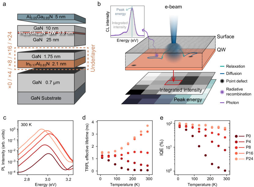
Sample preparation and macroscale characterisation. We grew our samples by metal-organic vapour phase epitaxy, using c-plane freestanding GaN substrates (dislocation density ) to minimise the influence of threading dislocations on our results. A lattice-matched In0.17Al0.83N/GaN superlattice (SL) was chosen as an underlayer to bury surface defects.[21, 27] Five samples with varying underlayer thickness were grown by changing the number of SL periods, —these samples are then labelled as P (Fig. 1a). An Al0.05Ga0.95N cap is included to avoid surface recombination.
These samples are tailored for high-resolution CL. During CL acquisition, the electron beam is raster-scanned over the sample surface, pausing regularly to gather data at evenly-spaced positions. At each position, the sample is locally excited while luminescence is globally collected—the full process is depicted in Fig. 1b. As the electron beam strikes the surface, electron-hole pairs generated within the excitation volume rapidly relax to the QW (green arrows in Fig. 1b), diffusing laterally (blue paths) until they reach a PD, or until they undergo radiative recombination. With continuous excitation, the carrier density within the QW reaches a steady-state spatial distribution, and photons (purple arrow) are emitted from radiative recombinations within this distribution. These photons are collected and dispersed in a spectrometer to obtain a CL spectrum for each excitation position in the scan—so called "hyperspectral" imaging (an example spectrum is shown in Fig. 1b). By fitting the QW emission at every position in this full spectral dataset (see supplementary Sec. I), we generate both a QW integrated intensity image and a peak emission energy image of the scanned area.
Since photons are globally collected, the CL spectrum recorded for one position is spatially averaged over a QW area related to (i) the carrier diffusion length and (ii) the excitation volume. These parameters are often not controlled in QW CL studies, which can limit the spatial resolution to hundreds of nanometres or more. Here, we discuss how we minimise both parameters in our samples to obtain high-resolution images.
Carrier diffusion lengths can be reduced by lower diffusion coefficients and shorter carrier lifetimes. The diffusion coefficient in InGaN/GaN QWs is mainly controlled by temperature, starting from near-zero at 10 K and increasing until it saturates at around 200 K.[28] Consequently, we reach the highest resolution at cryogenic temperatures. We also decrease diffusion lengths by choosing a very thin single QW of only three molecular monolayers ( 0.8 nm, Fig. 1a), which reduces the carrier radiative lifetime in the well.[29]
To minimise the excitation volume we use an electron-beam acceleration voltage of only 1.5 kV. At this voltage 95 % of the incident energy is absorbed within the top 20 nm of the sample (supplementary Sec. II), so we select a thin 10 nm top GaN layer to excite as close to the QW as possible (Fig. 1a).
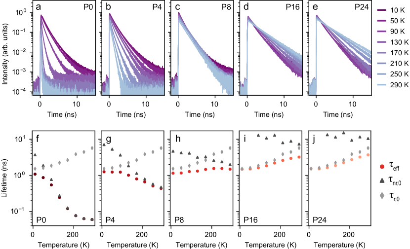
Before moving on to CL results, let us initially gauge the macroscale properties of our samples by more conventional methods for comparison. The room-temperature photoluminescence (PL) spectra shown in Fig. 1c clearly demonstrate the rise in QW efficiency achieved by the underlayer, with the peak intensity increasing by over two orders of magnitude from P0 to P24 (minor shifts in peak energy between different samples are explained in supplementary Sec. VI). This efficiency improvement is underscored by the striking contrast in QW effective lifetimes, gained from fitting time-resolved PL (TRPL) decay curves at early delays (Fig. 1d) (see supplementary Sec. III for decay curves). The lifetime behaviour of P24 indicates it is dominated by radiative recombination across the full temperature range, since it exactly matches radiative lifetime behaviour in an ideal QW.[30, 31, 32, 33] For other samples, as the number of SL periods is reduced the high-temperature effective lifetimes decrease due to thermal activation of defect-assisted recombination.[34, 35] The difference in IQE between the samples can be quantified with a simple treatment comparing the initial TRPL decay curve intensity to the effective lifetime (supplementary Sec. III).[36] Results are displayed in Fig. 1e: as expected, P24 maintains a high IQE of 64 3 % at room temperature, which matches that measured for a similar sample in another study.[27] Samples with fewer SL periods present much lower efficiencies, with the IQE of P0 falling to only % at room temperature. Overall, the results presented in Figs. 1c-e confirm that the defect density in the InGaN/GaN single QW significantly reduces on going from P0 to P24. With only these measurements, however, it is very difficult to precisely quantify the defect density, let alone identify their nature.
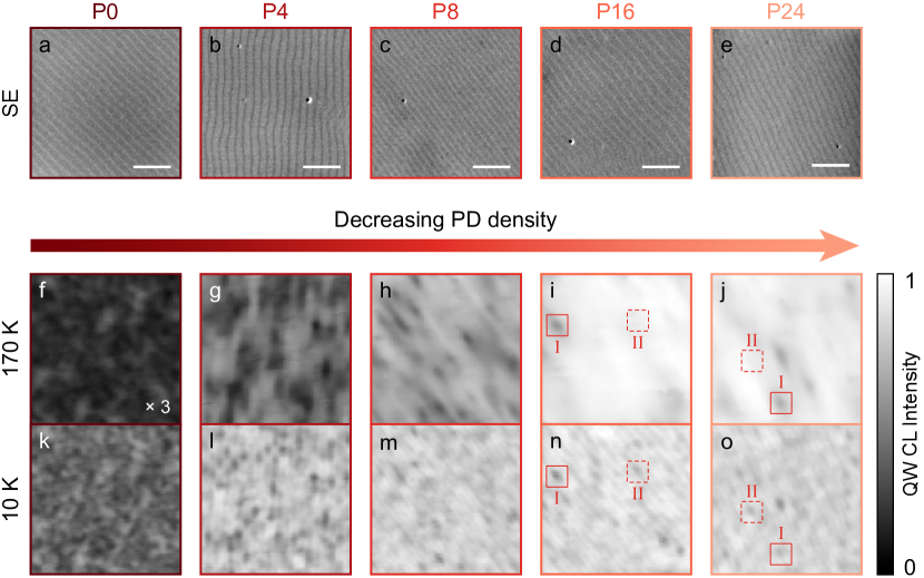
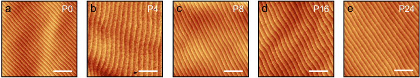
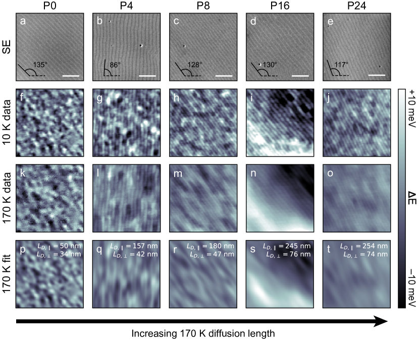
Cathodoluminescence. To spatially resolve and directly analyse the PDs, we turn our attention to CL results (Fig. 2). Atomic-height step-edges are noticeable in the secondary electron (SE) images (Figs. 2a–e) as a series of parallel lines; all samples present the same terraced morphology, indicating ideal step-flow growth (see supplementary Sec. IV for complementary atomic force microscopy). In addition, very few dislocation-induced V-shaped pits are visible due to the growth on freestanding GaN substrates.
We focus on CL integrated intensity images obtained by fitting the QW emission from hyperspectral data (Figs. 2f–o). Two temperatures were chosen for CL characterisation: 10 K, at which the diffusivity in the well is near zero so resolution is only limited by the excitation volume,[28] and 170 K, which allows us to probe the high-temperature regime while retaining sufficient signal-to-noise ratio for the most defective samples. The images obtained at 10 K and 170 K for each sample are from precisely the same area displayed in the SE images. The electron-beam probe current was set to 200 pA, which results in a steady-state carrier density near the peak-IQE condition for high quality InGaN/GaN QWs (see carrier density section and supplementary Sec. II).
We observe the impact from defects as local regions of low intensity in the 170 K results (Figs. 2f–j). Since dislocations identified in the SE images do not correlate with the dark regions, we attribute this low intensity to non-radiative recombination at PDs buried in the QW. The density of dark spots clearly decreases with increasing SL periods, directly indicating a decline in PD density in accordance with the PD-reducing behaviour of the underlayer.[21] Thus these CL images reveal the nanoscale origin of the increasing IQE from P0 to P24 in Fig. 1e. The elongated shape of PD dark regions in the less defective samples (Figs. 2h–j) is a result of asymmetric diffusion in the QWs as discussed further in the diffusion analysis section of this paper.
Upon cooling to 10 K (Figs. 2k–o), the impact from PDs is noticeably suppressed, as expected since the reduction in diffusion length means less carriers can reach PDs. Non-radiative recombination at defects also usually requires multiple-phonon emission, which is less likely at low temperatures.[34] Nevertheless, we still see some influence of PDs on the QW intensity. Observing effects from defects at cryogenic temperatures is not surprising: even at 10 K the IQEs of the more defective samples are only 70 % rather than 100 % (Fig. 1e). Such non-radiative recombination at low temperatures has previously been explained through tunneling-assisted transitions to defect levels.[35] With the improved spatial resolution of under 90 at this temperature (supplementary Sec. II), we can be confident we are observing individual PDs as long as densities remain below .
Comparing the 10 K and 170 K results for P16 and P24 (Figs. 2i, j, n, & o), we can distinguish two different types of PD: one type leads to greater local intensity reduction at high temperature (type-I, solid red box), while the other has much less effect (type-II, dashed red box). With a clear decrease in the number of dark regions at 170 K with increasing SL periods, we can already suggest the type-I defect density is reduced by the underlayer. However, actually quantifying the density of each type of defect requires a more detailed analysis of the CL images.
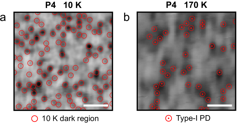
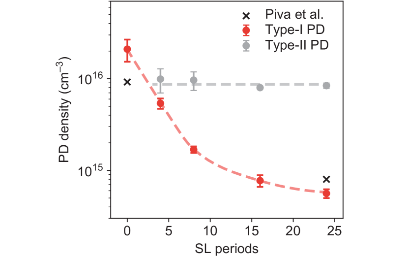
PD identification and counting. To estimate PD densities, we need to differentiate the two kinds of PD using their contrasting high-temperature behaviour as a criterion. This task is made more challenging by the loss of spatial resolution at 170 K due to increased carrier diffusion. Nonetheless, we can use 10 K images to accurately determine the position of PDs since diffusion length is near zero at this temperature. Therefore, we established a general two-step procedure: (i) use the Laplacian of Gaussian (LoG) method[38] to automatically detect dark regions in a 10 K image, then (ii) superimpose the positions of these regions on a 170 K CL image of the same sample area. If a position is associated with an intensity below a defined limit at 170 K, , it is identified as a type-I defect due to their strong impact at high temperature. For more information on our choice of reasonable and adapting the method for low defect densities in P16/P24, see supplementary Sec. V. An example of the procedure applied to P4 is shown in Fig. 3. While this procedure may not detect and correctly identify every PD, its design ensures reproducibility and avoids bias arising from counting/differentiating PDs manually. Once we have the 2-D defect densities from this method, we can calculate the 3-D densities using the full-width-at-half-maximum of the QW indium profile measured by scanning transmission electron microscopy (supplementary Sec. VI), since the PDs are contained within the well.
The final calculated PD densities are shown in Fig. 4. We note that for P0 the very high concentration of type-I PDs overwhelmed any effect from type-II PDs, preventing the estimation of the type-II defect density. With a decrease in the concentration of type-I defects in the QW from to only with increasing SL periods, we propose that type-I PDs are the key defects incorporated into the underlayer. In contrast, the concentration of type-II PDs is rather insensitive to the underlayer thickness. We conclude that the drastic increase in room-temperature IQE from P0 to P24 (Fig. 1(e)) is entirely due to the reduction in type-I PD density, while type-II defects have only a minor effect. The strong impact of type-I PDs on CL intensity and IQE indicates they possess energy levels near the middle of the InGaN bandgap, since such midgap states are known to be efficient non-radiative recombination centres.[2, 39]
Our CL-derived type-I PD densities are in good agreement with previous results from macroscale measurements by Piva et al.[37] (Fig. 4), which corroborates that we are spatially resolving individual PDs. Furthermore, their results also associate these defects with a near-midgap energy level, and identify another energy level near the valence band edge which could match our type-II defects. Other macroscale studies have also detected two types of PDs in InGaN/GaN QWs.[17, 19] Evidence suggests midgap (type-I) defects are intrinsic nitrogen vacancy complexes,[21, 40] while the type-II defect may be linked to impurities such as oxygen or carbon.[41] All these results highlight the versatility of our CL analysis to extract this information directly from images of PDs, and have particular relevance for III-nitride devices based on InGaN.
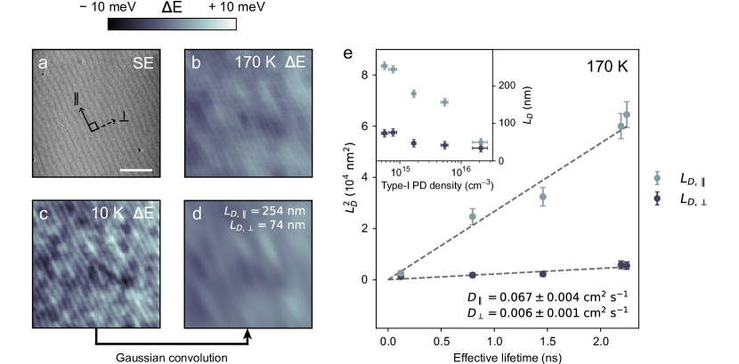
Diffusion analysis. Carrier dynamics within QWs is also of major relevance to optoelectronic devices. CL has been used to gauge carrier diffusion through various methods, often requiring a specific metallic mask, reference samples, or precise knowledge of the excitation volume.[42, 43, 44, 45] Here we estimate diffusion lengths without having to take any new measurements, but instead from a direct analysis of the hyperspectral maps we already used to generate the images in Fig. 2. This allows us to investigate the impact of non-radiative PD density on carrier diffusion, which was recently highlighted as an area where studies are lacking.[46]
At 10 K carriers in InGaN/GaN QWs have near-zero diffusivity, and therefore negligible diffusion lengths. As the temperature is raised, the diffusion constant increases before saturating at K.[28] The resulting increase in diffusion length reduces the spatial resolution at higher temperatures, as shown in Fig. 2 comparing the 170 K images to those at 10 K.
Neglecting drift effects, carriers injected into the well diffuse from each point into 2-D Gaussian distributions, with a standard deviation, , linked to the diffusion length, , by .[47] We can therefore straightforwardly model the effect of diffusion on our CL images by convoluting the negligibly diffused 10 K images with 2-D Gaussians. Using the convolution Gaussian’s as a fitting parameter, we can fit each 10 K image to the 170 K image of the same area, extracting at 170 K from the optimum fit for each sample. This method analyses average 2-D diffusion across the entire image, rather than inspecting only one local feature.
Using the CL intensity for this procedure is not ideal, as we cannot easily account for the thermal activation and complex behaviour of non-radiative recombination at PDs. Instead, we use the QW peak energy images of the same areas as in Fig. 2, which are directly "smoothened" as the diffusion length increases. The importance of using CL emission energy rather than intensity for diffusion analysis has been emphasised for the case of threading dislocations in GaN.[46] Since we are not interested in macroscopic changes in the peak energy with temperature, we subtract the mean peak energy from each image to map deviation from average peak energy, . These images then reflect inhomogeneity across the QW.
An example of this diffusion analysis being applied to P24 is shown in Figs. 5a–d (see supplementary Sec. VII for diffusion analysis of all samples). Inspecting Fig. 5c, we observe modulation in the QW emission energy by meV with the same periodicity as the step-edges in the SE image (Fig. 5a). While this modulation likely originates from the impact of step-edges on the bottom interface of the well,[48] it is beyond the scope of this study. However, this energy modulation has a direct influence on the carrier dynamics within the QW by presenting an energy barrier to diffusion perpendicular to the step-edges. This leads to anisotropic carrier diffusion in the QW, which we account for by adjusting the convolution Gaussian to contain two different perpendicular standard deviations. One standard deviation was fixed parallel to the step-edge direction, resulting in a diffusion length , while the other was set perpendicular to the step-edges, giving . The fitting result from convolution of the 10 K energy map is shown in Fig. 5d, and compares well with the real 170 K data (Fig. 5b). The computed values for the diffusion lengths confirm the anisotropic diffusion, with being over three times larger than . This step-edge induced anisotropy is likely stronger in our QWs since the effect of interface roughness on the carrier confinement energy is magnified for thinner wells.
and for all samples are plotted against their type-I PD densities in the inset of Fig. 5e. We can see that every sample exhibits anisotropic diffusion. Crucially, both and are severely limited by large PD concentrations, with decreasing by over 80 % from P24 to P0. In other words, despite the increased diffusion coefficient at raised temperatures, carriers in the more defective samples are unable to diffuse far since they quickly undergo non-radiative recombination at PDs. We can link this trend to the effective lifetimes gained from TRPL (Fig. 1d), , through where is the diffusion coefficient at 170 K. We note here that the TRPL excitation was carefully chosen to induce an initial QW carrier density in the same order of magnitude as the carrier density in our CL measurements ( , see supplementary Sec. II), so TRPL effective lifetimes should be comparable to carrier lifetimes in CL. The result from fitting this equation to our data is shown in Fig. 5e, with extracted diffusion coefficients underscoring the highly anisotropic diffusion in our QWs. , which represents unrestricted diffusion in the well, is in reasonable agreement with diffusion coefficients previously found for InGaN/GaN QWs.[28] With this analysis, we have demonstrated that a straightforward and general CL data treatment can measure diffusion lengths with only two fitting parameters and no assumed constants. Furthermore, PD density is confirmed as a critical parameter controlling diffusion in QWs, re-emphasising that high IQE samples are required to study intrinsic carrier dynamics.
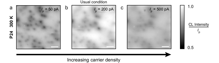
Influence of carrier density on point defects. The impact of non-radiative defects on the IQE of QWs is known to depend strongly on the carrier density.[49] CL measurements using continuous excitation produce a local steady-state carrier density, which increases with the generation rate and lifetime of the carriers. Since the generation rate is proportional to the CL electron-beam probe current, ,[50] this current directly affects the carrier density in the QW—yet is not commonly varied in CL defect studies.
In Fig. 6, we investigate how carrier density alters the sensitivity of CL to PDs by mapping the QW intensity on the same area of P24 at three different probe currents. Due to the low density of type-I defects in P24, the images can be taken at a higher temperature and larger scale than previous results while still being able to resolve PDs. The images are normalised relative to to give an indication of how IQE is affected. On increasing , the impact from PDs is greatly reduced since defect-assisted non-radiative recombination usually dominates at lower carrier densities.[49] As the carrier density is increased, radiative recombination and then Auger recombination progressively play larger roles. Both of these processes are unlikely to be strongly spatially correlated with defects, and hence they suppress any influence of PDs on the CL intensity as in Fig. 6c. We note that the brightness of the pA image (Fig. 6b) suggests this condition is near peak-IQE, in agreement with the calculated steady-state CL carrier density of (see supplementary Sec. II).
Looking back at Figs. 2f–j, we can now understand why the influence of each PD on the CL intensity appears weaker and more "washed-out" for the samples with a low type-I PD concentration, i.e., P16 and P24. As previously explained, the steady-state density in each sample’s well scales with its carrier lifetime. Due to their longer lifetimes at high temperatures (Fig. 1d), at 170 K the CL carrier density in P16/P24 is higher than in the more defective samples. Consequently, this large steady-state carrier density leads to decreased sensitivity to PDs in a similar way to what we see in Fig. 6. As well as directly demonstrating the dependence of PD non-radiative recombination on the carrier density, these results emphasise that probe current, though often overlooked, must be carefully selected for optimal defect imaging in CL.
In summary, combining CL at an acceleration voltage of only 1.5 kV with specific sample design, we spatially resolved and analysed individual non-radiative PDs buried in InGaN/GaN single QWs. Using just two hyperspectral maps of each sample at different temperatures, we extracted information on PD types, PD densities, and carrier diffusion lengths, all through direct observation and straightforward analysis methods. We identified two different types of PD: near-midgap defects with a strong impact on CL intensity and IQE which can be incorporated into an indium-containing underlayer (type-I), and defects with a lesser impact on efficiency which are not affected by the underlayer (type-II). The density of type-I PDs was estimated to range from up to with decreasing underlayer thickness, highlighting the capability of our methodology to image PDs even up to high densities. With careful experimental methods, we investigated the interplay between carrier dynamics and PDs. We measured diffusion lengths from CL peak energy images, demonstrating their dependence on the PD concentration, and showed that carrier density significantly affects the influence of PDs on CL intensity. Overall, this comprehensive study serves as a proof-of-concept for imaging and directly analysing PDs in QWs, and lays the foundation for advanced future studies such as applying time-resolved CL to a single buried PD.
Methods
Sample growth. The samples were grown by metal-organic vapour phase epitaxy in a horizontal Aixtron 200/4 RF-S reactor on n-type c-plane freestanding GaN substrates (dislocation density ). After a low-temperature GaN buffer, 700 of GaN is deposited at 1000 using trimethylgallium with H2 as the carrier gas. Then, the temperature is decreased to 770 , and the carrier gas is switched to N2 for the growth of the In0.17Al0.83N SL, using trimethylindium and trimethylaluminium. Triethylgallium is used for the GaN layer in the SL. This lattice-matched In0.17Al0.83N/GaN SL was used as the underlayer since it was demonstrated to produce near-ultraviolet LEDs with improved IQE compared to bulk underlayers.[27] A 10 GaN spacer is grown at the same temperature with triethylgallium. Up to this point, the structure is mostly grown with Si doping at around ; however, the last two periods of the SL and the first 5 of the following GaN barrier are highly doped with Si ( ) to screen the electric field arising from the spontaneous polarisation mismatch at InAlN/GaN interfaces (see supplementary Sec. VI).[27] The rest of the structure (see Fig. 1a) is grown under similar conditions but with no intentional doping. The InGaN/GaN single QW has a nominal indium content of 15 %.
Photoluminescence. The room-temperature QW PL was measured for each sample using a 325 HeCd laser at a power density of 2.0 . For TRPL, we used the third harmonic of a mode-locked Ti:sapphire laser emitting 100 fs pulses at 266 with a repetition rate tuned to 7.6 MHz to measure extended PL decay times. An excitation density of 5 was applied using a 40x reflective objective. Detection was performed using a time-correlated single-photon counting system with an avalanche photo-diode. Decay curves were measured at five different energies across the QW emission before being summed to give the final curves; this ensures any carrier transfer to different energies in the QW has a limited impact on our measured lifetimes. Effective lifetimes were calculated by mono-exponentially fitting these decay curves at early delays accounting for the instrument response function. The decay time resolution limit of this system is around 50 .
Cathodoluminescence spectroscopy. CL imaging was performed using a CL-dedicated scanning electron microscope system (Attolight Rosa 4634) with the acceleration voltage set at 1.5 kV. For most measurements (apart from those in Fig. 6) the e-beam was raster-scanned in steps of 18 with an integration time of 3 and a probe current of 200 pA. A Cassegrain reflective objective was used to collect the light and direct it towards a spectrometer, with a grating of 600 lines per and a blaze-wavelength at around 300 nm. The dispersed light was then sent to a cooled charge-coupled device camera to record a full intensity-energy spectrum at every pixel (hyperspectral imaging). The QW emission at every pixel was fully fitted, allowing us to generate the QW CL intensity and peak energy images shown in this work. The fitting function was a combination of three Gaussians to fit the main QW peak and subsequent longitudinal-optical phonon replicas (see supplementary Sec. I). Temperature control was achieved using an open-flow helium cryostat. SE images taken at different temperatures on the same sample area were precisely aligned by finding the relative pixel shifts which maximised the cross-correlation value—applying these same shifts to the simultaneously-acquired hyperspectral maps then spatially aligned the CL data. All hyperspectral analysis was carried out using the hyperspy package in Python.[51]
Data availability. The datasets generated during and/or analysed during the current study are available from the corresponding author on reasonable request.
Acknowledgements
This work was supported by the Swiss National Science Foundation through Grant No. 200021E 175652. The CIME at EPFL is acknowledged for access to its facilities, and Dr. B. Bártová at CIME is thanked for the focused ion beam preparation. We thank N. Tappy (EPFL), Dr. C. Haller (EPFL), and Prof. C. Hébert (EPFL), for useful discussion.
Author contributions
J.-F.C. grew the samples. T.F.K.W. performed the room-temperature PL measurements, while T.F.K.W. and W.L. carried out the CL measurements. V.O. performed all TRPL measurements with R.A.T. D.T.L.A. carried out the scanning transmission electron microscopy characterisation. T.F.K.W. was responsible for all analysis carried out on the raw data from the above measurements. T.F.K.W., R.B., and N.G. wrote the paper. N.G. conceived and directed the project. All authors discussed the results and commented on the manuscript.
Additional information
Supplementary Information accompanies this paper.
Competing interests: The authors declare no competing financial interests.
SUPPLEMENTARY INFORMATION
CATHODOLUMINESCENCE HYPERSPECTRAL FITTING
As mentioned in the main text, QW CL integrated intensity and peak energy maps were obtained from hyperspectral maps by fitting the CL spectrum at each pixel. All fitting was done using the hyperspy package for Python.[51] An example CL spectrum taken from a hyperspectral map of P16 is shown in Fig. S1. The emission shape is very characteristic for InGaN/GaN QWs with significant inhomogeneous broadening and clear longitudinal-optical (LO) phonon replicas at lower energies. Due to the large inhomogeneous broadening, the spectra are well fitted by using three Gaussians: one for the main peak, and two for the subsequent LO phonon replicas. To minimise free parameters, we fixed the peak energy separation of these three Gaussians at 92 meV to agree with the LO phonon energy in wurtzite GaN.[52] The peak intensities of the phonon replicas were fixed to that of the main peak using the Huang-Rhys factor as a fitting parameter.[53] Finally, the full width at half maxima (FWHMs) of the phonon replicas were fixed to be equal—this left the model with only five free fitting parameters. The best fit using this model is shown in Fig. S1, with each individual Gaussian component also plotted.
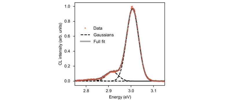
With accurate heteroscedastic noise estimation, we obtained reduced chi-squared () values for every spectrum fitted. All hyperspectral maps fitted in this study had an average in the range 0.9–1.6, confirming the suitability of our model.
CARRIER INJECTION IN CATHODOLUMINESCENCE
Fig. S2a shows the interaction volume of the electron beam at an acceleration voltage of 1.5 kV, gained from a Monte-Carlo simulation. For this simulation, we estimated the electron probe diameter at the sample surface by inspecting the SE images in Fig. 2 of the main text. Specifically, we set the FWHM of the probe to the average FWHM of surface step-edges ( nm), since these step-edges should be near-atomically sharp. Although this is a conservative estimate, the probe diameter is expected to be larger at low acceleration voltages due to enhanced chromatic aberration, particularly in a system lacking beam deceleration such as ours. The potential loss in CL signal resolution due to the increased probe diameter compared to higher acceleration voltages is negligible given the reduction in interaction volume this low acceleration voltage provides.
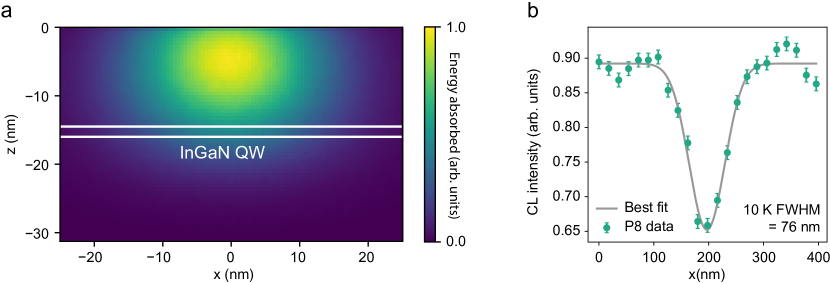
From Fig. S2a, we can see that the vast majority of the excitation energy (95 %) is absorbed in the top 20 nm of the sample, hence the InGaN/GaN single QW is placed only 15 nm below the surface. This design ensures all generated carriers are able to reach the QW in the entire temperature range we explore, since the carrier diffusion length in GaN is always above 15 nm from 10 K up to 300 K.[55, 56, 46] In addition, using thin top layers limits any lateral carrier spreading that can occur before the carriers relax to the QW. The radial FWHM of the interaction volume in Fig. S2a is around 25 nm, which indicates the maximum achievable CL resolution if there were no lateral carrier diffusion. Thus we could expect this to match the CL resolution of our 10 K images, since the diffusion length should be near-zero in the QW as emphasised in the main text.
To compare the results of the Monte-Carlo simulation to our experiments, we inspect the 10 K QW CL intensity across one PD as shown in Fig. S2b (taken from Fig. 2m in the main text). Since the PD itself is localised on one point in the QW, the FWHM of this profile indicates the real resolution in the QW at 10 K. The experimentally measured resolution, at 76 nm, is larger than the 25 nm that was expected from Fig. S2a. This discrepancy is confirmed by repeating the analysis for different PDs, with an average 10 K intensity profile FWHM of nm.
The mismatch is explained by two factors. Firstly, a recent study by Jahn et al. has evidenced an increase in CL interaction volumes compared to Monte-Carlo simulations,[57] since CL generates hot carriers which can only radiatively recombine once they have lost excess energy through phonon emission. They well-described the interaction volume broadening in GaN by convoluting the Monte-Carlo radial profile by a Gaussian with FWHM of about 50 nm. Secondly, as previously mentioned, there will be some lateral carrier diffusion in the top barrier of the sample before carriers fully relax to the QW. With random diffusion, we expect this effect to broaden the final 2-D carrier distribution in the QW on the order of the thickness of the barrier, i.e., 15 nm. Combining both of these factors with our original 25 nm Monte-Carlo FWHM, we arrive at a more realistic resolution estimate of nm, much closer to our measured value of nm. The remaining difference of 10–30 nm could then be due to the limited diffusion possible within the QW at 10 K, with a diffusion coefficient of far less than 0.01 .[28] Such low levels of diffusion at 10 K would only slightly impact our calculated QW diffusion lengths at 170 K, since these are mainly on the order of 100s of nanometres.
The nm FWHM of the CL intensity profile around single PDs should also be close to the FWHM of the carrier density distribution at 10 K in the QW. Meanwhile we can estimate the total generation rate, (), of carriers in CL through the well known equation:[50]
| (S1) |
where is the electron beam probe current, is the charge of an electron, is the bandgap of the sample, and is the average energy deposited per electron in the sample, which is equivalent to the beam energy minus the energy lost through backscattered electrons (calculated from Monte-Carlo simulations).[54] Using our estimated steady-state carrier distribution FWHM, , and assuming this distribution is Gaussian-like, we can then write the peak steady-state carrier density in the QW, , as:
| (S2) |
if we assume all generated carriers relaxed to the QW, with being the carrier lifetime. Into eq. S2 we input pA, eV, nm, and the calculated keV. For , we use the effective lifetime gained from TRPL results at 10 K ( ns, see next section). The resulting is found to be . This calculated density is important when considering the comparison of CL diffusion lengths and TRPL effective lifetimes in Fig. 5 of the main text, as described in the next section. We note that peak IQE for high-quality InGaN/GaN QWs commonly occurs at about this carrier density,[49] which is in good agreement with what we observe in Fig. 6 of the main text, in which the highest CL intensity-probe current ratio is achieved at pA. Conversely, at pA we expect a carrier density in the range while for pA it should be closer to —these densities are further into the defect dominated and Auger recombination regimes, respectively.[49]
TIME-RESOLVED PHOTOLUMINESCENCE
In Fig. 1 of the main text, data extracted from QW TRPL decay curves are presented: here we show the original curves in Figs. S3a–e. The evolution of PL intensity, , with time, , in these decay curves is described by the function:
| (S3) |
where is the initial carrier density in the well, is the carrier radiative lifetime, is the total carrier lifetime, and is a constant related to the collection efficiency, area of sample excited, and integration time. is related to and the non-radiative lifetime, , through:
| (S4) |
Unfortunately, and often depend on carrier density in a non-straightforward manner.[58, 49] Since the carrier density in TRPL decreases as time progresses, this dependence leads to deviation from mono-exponential decay as we see in Figs. S3a–e. To simplify our analysis, we obtained the effective lifetime, , for each curve by fitting intensity at early delay times with a mono-exponential decay convoluted with the instrument response function. is then equivalent to the true carrier lifetime, , only when the carrier density is around . With an excitation density of 5 at a laser wavelength of 266 nm, and making the simplifying assumption that nearly all carriers relax to the QW, is on the order of . Crucially, this is the same order of magnitude as the steady-state carrier densities in our CL measurements (see previous section), allowing us to use our calculated as a reasonable approximation for the carrier lifetime in CL, as we did in the diffusion analysis of the main text and in the previous section of this supplementary. As mentioned previously, this carrier density should also be near peak-IQE conditions for high-quality InGaN/GaN QWs.[58, 49]
To calculate the macroscopic IQEs as presented in Fig. 1e of the main text, we used a method first applied by Langer et al.[36] Eq. S3 indicates that using the initial intensity of a decay curve, , we can calculate the initial radiative lifetime, , at any temperature, , through:
| (S5) |
Since excitation and detection conditions aren’t changed, and will be near-constant across all temperatures as long as the intensity rise time is much less than . Hence, if we have at one temperature, we can compute , which then lets us calculate for all temperatures. Having already found , we can then determine through eq. S4. Finally, the IQE is given by:
| (S6) |
The next step is to estimate at one temperature. To this end, we look more closely at the temperature-dependence of P24 (Fig. S3j). The lifetime of P24 increases linearly above 90 K from 1.6 up to 3.7 at room temperature. Such behaviour is expected for in any direct bandgap semiconductor QW for both free electron/hole pairs and excitons.[30, 32] Meanwhile below 90 K, the lifetime is temperature-independent, indicating that the majority of carriers are localised in this temperature range due to alloy disorder in the InGaN/GaN QW.[31, 33] The consistency of P24’s behaviour with that expected for indicates this sample is dominated by radiative recombination across the full temperature range we explore. Given that defect-assisted non-radiative recombination is a thermally-activated process,[34] we can safely assume that for P24 is very close to at 10 K ( ns). We use this value as for all samples, since they are expected to have the same radiative lifetime behaviour due to identically grown QW structures.
With this key, we can now calculate for all samples using the process described above. The main source of random error in this method derives from small changes in optical alignment altering the value of . We minimise the error by averaging across the samples, which is reasonable since they should all have similar radiative lifetimes. P0 is excluded from this average since at high temperatures its becomes very short (Fig. S3f). This leads to highly inaccurate estimation since (i) is on the order of the rise time, significantly decreasing from its low-temperature value, and (ii) reaches the resolution limit of the detection system, and is therefore an overestimation of the true lifetime.
ATOMIC FORCE MICROSCOPY
Fig. S4 presents complementary atomic force microscopy (AFM) images for all samples in this study. The observed morphology matches that of the SE images in Figs. 2a–e of the main text, with step-edges evenly spaced by about 80–100 nm. The step-edge height is nm, equivalent to two molecular monolayers of GaN.[59] This places the substrate misorientation in the range 0.3∘–0.4∘, close to the nominal misorientation of 0.2∘. AFM underscores the low density of threading dislocations in these samples, with no surface V-pits visible at this scale of .
POINT DEFECT COUNTING DETAILS
The PD identification and counting procedure used in the main text involves three parameters: the FWHM of the Gaussian filter () and the detection threshold () involved in the LoG method applied at 10 K, along with the intensity limit () defined for the 170 data. is linked to the size of the dark regions that will be detected by the LoG method. was always fixed at 0.025 to avoid detecting random noise in the CL images as defects.
To define a reasonable for each sample, we calculated the 170 CL intensity histograms from the images in Figs. 2f–j of the main text. P4 and P8 show distinct double-humped distributions (Fig. S5a), as is expected from the influence of two different types of PD. Fitting both distributions with two Gaussians then separates the contribution from type-I and type-II defects. The peaks of the lower intensity Gaussians are taken to define for each sample, in accordance with the greater impact of type-I defects on 170 CL intensity.
The other samples do not exhibit double-peaked distributions since they are dominated by only one type of defect. P0 exhibits a distribution skewed to low intensities, due to the high density of type-I PDs overwhelming any impact from type-II PDs. In this case, we make the simplifying assumption that all 10 K intensity fluctuations detected by LoG correspond to type-I defects for P0. The results in Fig. 4 of the main text for the P0/P4/P8 type-I and type-II PD densities were obtained by applying our method to the images in Fig. 2 of the main text, with the errors estimated by varying in the range nm—this range matches the CL resolution at 10 K ( nm, see Sec. II).
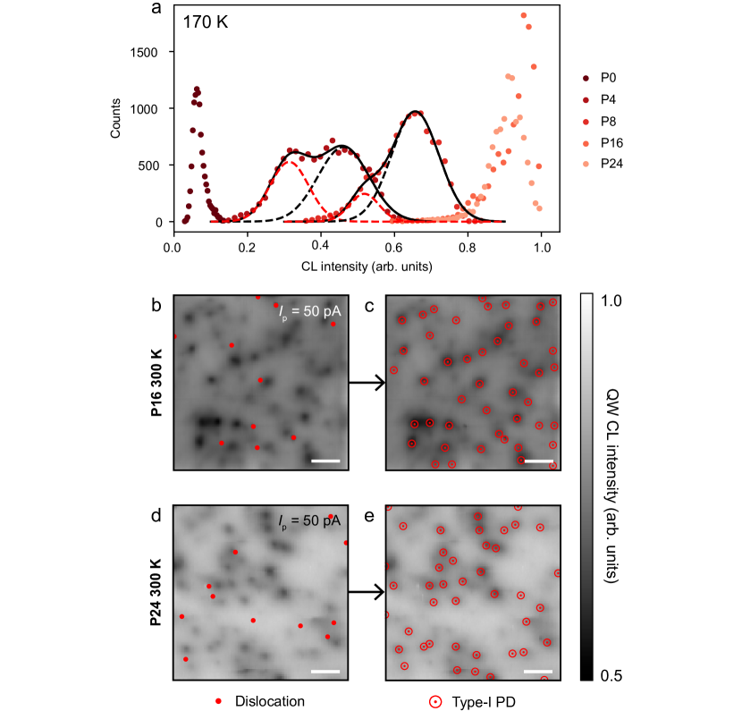
On the other hand, the P16/P24 170 K images have distributions skewed towards high intensity, since (i) there are nearly no type-I PDs at this scale and (ii) the higher carrier density in these samples minimises the impact of PDs (see Fig. 6 in the main text). To counteract both of these effects, we analysed larger CL intensity images of P16/P24 at a low probe current, , of 50 pA (Figs. S5b–e). We further enhanced the impact of type-I PDs by heating the samples to room temperature. At this temperature type-II PDs will have no resolvable effect on the intensity, so dark areas will correspond to type-I defects and we do not need to define . This option was not available for the other samples since the longer diffusion length at high temperature combined with the high density of type-I PDs would have made individual defects unresolvable.
At this large scale, there are more threading dislocations in the analysed area which we must not falsely identify as PDs, hence we highlight dislocation positions in Figs. S5b & d (as linked to V-pits in the corresponding SE images). There is no clear spatial correlation between the dislocation positions and any dark spots in the CL intensity. This emphasises the dominant role played by PDs in these QWs compared to dislocations, and allows us to safely apply LoG detection to these images to calculate type-I PD density without counting any dislocations (Figs. S5c & e). For error estimation, was varied in the range nm accounting for the much greater diffusion length at higher temperatures (c.f., P24 has diffusion length nm at 170 K, see Fig. 5 in the main text). Taking the difference between this type-I density and the density of 10 dark areas in Figs. 2n & o of the main text then allowed us to calculate the P16/P24 type-II PD densities.
The final number of type-I and type-II PDs counted in this work, and the area they were counted over, is listed for each sample in Table S1. We note that the low uncertainty for the P8 type-I density is a consequence of the low number of defects counted for this sample, and is very likely an underestimation.
| Sample | Type-I PD counted | Type-II PD counted | Area analysed () |
| P0 | 0 (No ) | 4 | |
| P4 | 4 | ||
| P8 | 4 | ||
| P16 | 49 (type-I); 4 (type-II) | ||
| P24 | 49 (type-I); 4 (type-II) |
TRANSMISSION ELECTRON MICROSCOPY AND TRANSITION ENERGY SIMULATIONS
To confirm the exact structure of our three-monolayer (ML) QWs, samples P0 and P24 were characterised by scanning transmission electron microscopy (STEM) energy-dispersive X-ray spectroscopy (EDX). The cross-section samples for STEM analysis were prepared by focused Ga ion beam lift-out using a Zeiss NVision 40. Before milling, the top surface was protected by depositing an amorphous carbon layer using an electron beam and then the ion beam. The samples were sectioned within a few degrees of the zone axis. Primary milling was made using a 30 kV ion beam, with final cleaning made using a 5 kV ion beam. The atomic resolution STEM imaging and EDX spectroscopy were done using a double-aberration corrected FEI Titan Themis 60-300, using a convergence semi-angle of 20 and a high tension of 80 kV in order to prevent electron-beam damage by the knock-on mechanism.[60, 61] A Fischione photomultiplier tube detector was used for taking the high-angle annular dark-field images, using an inner collection semi-angle of 50 . The resolution of the images is 1.25–1.5 . EDX hyperspectral data were acquired using FEI Super-X ChemiSTEM detectors with FEI/Thermo Scientific Velox software; this software was also used to record the STEM images and for making the EDX data analysis. In order to gauge the thickness of the STEM samples, and as a check on EDX results, complementary STEM electron energy-loss spectra were acquired using a Gatan GIF Quantum ERS spectrometer: the measured thicknesses were 70 and 40 for P0 and P24, respectively.
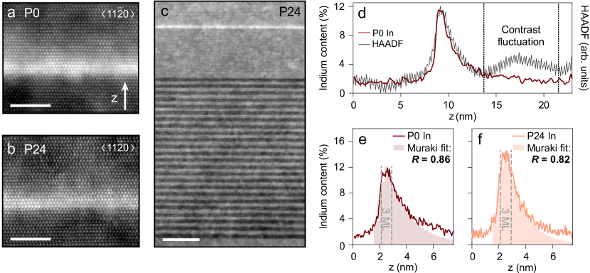
Fig. S6 presents the results, starting with atomic-resolution high-angle annular dark-field (HAADF) images of the P0 and P24 QWsFigs. S6a & b. The QWs are close to the nominal thickness of three MLs, but their interfaces are not completely sharp. However, this observation may be affected by contrast fluctuations which are unrelated to indium content. Fig. S6c shows a large scale HAADF-STEM image of P24 with contrast fluctuations across the entire sample, seemingly having no correlation with any individual part of the structure. These fluctuations are almost certainly an artefact: comparing indium content extracted from EDX spectroscopy with the HAADF profile across the QW (Fig. S6d) near a typical fluctuation, we observe that the HAADF contrast fluctuation does not correspond to any change in indium concentration. These fluctuations may be due to surface relaxation or contamination from sample preparation; at an acceleration voltage of only 80 kV, the electron beam is sensitive to any potential surface effects. To avoid this artefact, we rely on EDX measurements rather than HAADF images: Figs. S6e & f display indium content profiles across the QWs of P0 and P24, obtained by averaging the EDX signal over the regions in Figs. S6a & b. Indeed there is a high plateau in the profiles exactly three MLs thick, but the QW top interface is not sharp—a characteristic of indium segregation during growth.
To quantify the indium surface segregation, we can apply a model developed by Muraki et al.[62] In this model, during the growth of one molecular ML of InGaN a certain fraction of the indium atoms at the surface are incorporated into the ML while the remaining fraction segregates to the new surface. As such, represents the degree of segregation that occurred during growth. The In content in the nth ML, , is then given by:
| (S7) | |||||
| (S8) |
where and are the nominal width and indium content of the QW, respectively. This model was fitted to the STEM-EDX results for the QWs of P0 and P24, as shown in Figs. S6e & f. Only the data for which the measured In content was greater than 5 % were considered for the fitting process; this was to avoid the % zero error present in the EDX measurement. The zero error arises from noise in the EDX spectra which is falsely quantified when the indium content is below the detection limit. The derived fit could then be extrapolated into the spurious regions, eliminating the error in subsequent analyses. was the same for both samples at 4.3, close to the target value of 3; meanwhile was 26 % for both samples. The values of extracted (0.82 and 0.86) are in line with previous estimations of the segregation coefficient in InGaN/GaN QWs.[63] Crucially, the QW of P0 possesses a slightly larger value than that of P24, indicating that greater indium segregation occurred in this sample. This could explain the PL redshift between P0 and P24 seen in Fig. 1c of the main text—to confirm, we carried out Schrödinger-Poisson calculations.
| P0 energy (eV) | P24 energy (eV) | Difference (meV) | |
|---|---|---|---|
| Experiment | 3.006 | 2.940 | 66 |
| Simulation | 3.117 | 3.068 | 49 |
For these calculations, the entire structures of P0 and P24 were simulated at 300 using nextnano,[64] including the accurate ML-by-ML QW indium profiles obtained from the Muraki fit. We can compare the simulated results for P0 and P24 to those gained from PL at room temperature using a HeCd laser (Table S2). The difference in transition energies between the QWs of P0 and P24 is predicted to be 49 at room temperature, which accounts quite well for the PL redshift observed between P0 and P24, supporting our structural analysis. However, a noticeable discrepancy exists between the experiment and simulated absolute values for each sample ( ). Multiple factors contribute to this discrepancy. Firstly, the simulation does not consider the exciton binding energy in the QW, which lowers the emission energy relative to the calculated transition energy. Taking GaN as an example, in the limiting exact 2D case of an infinitely deep QW the exciton binding energy is increased by a factor of four relative to the bulk value, placing it at around 100 .[59] Secondly, a Stokes shift is expected between absorption and emission energies due to tail states within the bandgap; this effect is further exacerbated by alloy disorder in the InGaN/GaN QW.[65] Finally, EDX quantification is never absolutely precise, and there is at least a at.% systematic error involved. All of these factors should be roughly constant for both samples, and hence do not impede the comparison between them.
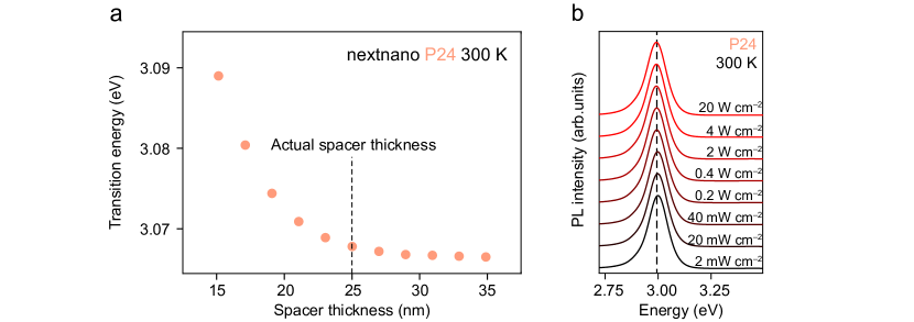
Finally, it was worth ruling out any effect on the fundamental QW transition energy from the electric field induced by the InAlN/GaN SL; as can be seen in Fig. S7a, at our GaN spacer thickness of 25 between the SL and QW the electric field of the SL has been mostly screened. Increasing the spacer thickness to 35 nm would result in a change in the transition energy of only . Furthermore, the absence of any impact from the built-in electric field can be verified experimentally by measuring PL spectra for P24 under various excitation power densities (Fig. S7b). Any effect from the electric field would be revealed as a blueshift in QW emission energy at higher power densities due to carriers screening the field. Conversely, we see that the peak emission energy remains constant across the entire power range, confirming that the 66 discrepancy in peak emission energy between P0 and P24 is not due to any electric field from the SL. Furthermore, this clearly demonstrates the limited effect of the quantum-confined Stark effect in our ultra-thin QWs; consequently, we do not need to consider any field-screening effects in in our probe current study (Fig. 6 of the main text).
In summary, this complete analysis ensures we can be confident in the segregated indium profiles measured by EDX and their corresponding Muraki fits. The analysis identifies marginally greater segregation in the QW of P0 compared to P24, which explains the observed PL peak energy difference between the samples (with any effect from the built-in electric field being ruled out experimentally and theoretically). Slight changes in segregation can then explain the small variances in peak energy between the samples seen in the room-temperature QW PL (Fig. 1c of the main text). For our calculation of PD 3-D densities () from 2-D values (), we use the average FWHM of the EDX indium profiles at nm.
COMPLETE DIFFUSION ANALYSIS
In Fig. 5e of the main text we presented the diffusion lengths calculated for all samples from the Gaussian convolution fitting method. Here we show the peak energy images used to obtain these diffusion lengths in Fig. S8. Step-edge directions were calculated by Fourier transform analysis of the SE images (Figs. S8a–e). The impact of the step-edges on the peak energy is evident for P4–P24 in Figs. S8g–j, which leads to strongly anisotropic diffusion in all of these samples. This is confirmed by the diffusion lengths parallel () and perpendicular () to the step-edges extracted by Gaussian convolution (Figs. S8p–t). These convoluted images are in good agreement with the real 170 K peak energy images (Figs. S8k–o), confirming the validity of our simple diffusion analysis. The error bars in diffusion length shown in Fig. 5 of the main text were estimated by varying the initial parameters of the Gaussian convolution fit.
References
References
- Bourgoin and Lannoo [1983] J. Bourgoin and M. Lannoo, Point Defects in Semiconductors II: Experimental Aspects (Springer-Verlag, Heidelberg, 1983).
- Shockley and Read [1952] W. Shockley and W. T. Read, “Statistics of the recombinations of holes and electrons,” Physical Review 87, 835–842 (1952).
- Thomas, Hopfield, and Frosch [1965] D. G. Thomas, J. J. Hopfield, and C. J. Frosch, “Isoelectronic traps due to nitrogen in gallium phosphide,” Physical Review Letters 15, 857–860 (1965).
- Wight [1977] D. R. Wight, “Green luminescence efficiency in gallium phosphide,” Journal of Physics D: Applied Physics 10, 431–454 (1977).
- Aharonovich, Englund, and Toth [2016] I. Aharonovich, D. Englund, and M. Toth, “Solid-state single-photon emitters,” Nature Photonics 10, 631–641 (2016).
- Bradac et al. [2019] C. Bradac, W. Gao, J. Forneris, M. E. Trusheim, and I. Aharonovich, “Quantum nanophotonics with group IV defects in diamond,” Nature Communications 10, 1–13 (2019).
- Kressel [1981] H. Kressel, “Semiconductors and semimetals volume 16,” (Academic Press, London, 1981) Chap. 1 The effect of crystal defects on optoelectronic devices.
- Ball and Petrozza [2016] J. M. Ball and A. Petrozza, “Defects in perovskite-halides and their effects in solar cells,” Nature Energy 1, 16149 (2016).
- Park et al. [2018] J. S. Park, S. Kim, Z. Xie, and A. Walsh, “Point defect engineering in thin-film solar cells,” Nature Reviews Materials 3, 194–210 (2018).
- Bourrellier et al. [2016] R. Bourrellier, S. Meuret, A. Tararan, O. Stéphan, M. Kociak, L. H. Tizei, and A. Zobelli, “Bright UV single photon emission at point defects in h-BN,” Nano Letters 16, 4317–4321 (2016).
- Sang et al. [2016] X. Sang, Y. Xie, M. W. Lin, M. Alhabeb, K. L. Van Aken, Y. Gogotsi, P. R. Kent, K. Xiao, and R. R. Unocic, “Atomic defects in monolayer titanium carbide (Ti3C2Tx) MXene,” ACS Nano 10, 9193–9200 (2016).
- Jiang et al. [2018] Y. Jiang, Z. Chen, Y. Han, P. Deb, H. Gao, S. Xie, P. Purohit, M. W. Tate, J. Park, S. M. Gruner, V. Elser, and D. A. Muller, “Electron ptychography of 2D materials to deep sub-ångström resolution,” Nature 559, 343–349 (2018).
- Feng et al. [2018] J. Feng, H. Deschout, S. Caneva, S. Hofmann, I. Lončarić, L. Predrag, and A. Radenovic, “Imaging of Optically Active Defects with Nanometer Resolution,” Nano Letters 18, 1739–1744 (2018).
- Edelberg et al. [2019] D. Edelberg, D. Rhodes, A. Kerelsky, B. Kim, J. Wang, A. Zangiabadi, C. Kim, A. Abhinandan, J. Ardelean, M. Scully, D. Scullion, L. Embon, R. Zu, E. J. Santos, L. Balicas, C. Marianetti, K. Barmak, X. Zhu, J. Hone, and A. N. Pasupathy, “Approaching the Intrinsic Limit in Transition Metal Diselenides via Point Defect Control,” Nano Letters 19, 4371–4379 (2019).
- Ziatdinov et al. [2019] M. Ziatdinov, O. Dyck, X. Li, B. G. Sumpter, S. Jesse, R. K. Vasudevan, and S. V. Kalinin, “Building and exploring libraries of atomic defects in graphene: Scanning transmission electron and scanning tunneling microscopy study,” Science Advances 5, eaaw8989 (2019).
- Rittweger et al. [2009] E. Rittweger, K. Y. Han, S. E. Irvine, C. Eggeling, and S. W. Hell, “STED microscopy reveals crystal colour centres with nanometric resolution,” Nature Photonics 3, 144–147 (2009).
- Armstrong et al. [2012] A. Armstrong, T. A. Henry, D. D. Koleske, M. H. Crawford, and S. R. Lee, “Quantitative and depth-resolved deep level defect distributions in InGaN/GaN light emitting diodes,” Optics Express 20, A812–A821 (2012).
- Armstrong, Crawford, and Koleske [2014] A. M. Armstrong, M. H. Crawford, and D. D. Koleske, “Contribution of deep-level defects to decreasing radiative efficiency of InGaN/GaN quantum wells with increasing emission wavelength,” Applied Physics Express 7, 032101 (2014).
- Armstrong et al. [2015] A. M. Armstrong, B. N. Bryant, M. H. Crawford, D. D. Koleske, S. R. Lee, and J. J. Wierer, “Defect-reduction mechanism for improving radiative efficiency in InGaN/GaN light-emitting diodes using InGaN underlayers,” Journal of Applied Physics 117, 134501 (2015).
- Haller et al. [2017] C. Haller, J.-F. Carlin, G. Jacopin, D. Martin, R. Butté, and N. Grandjean, “Burying non-radiative defects in InGaN underlayer to increase InGaN/GaN quantum well efficiency,” Applied Physics Letters 111, 262101 (2017).
- Haller et al. [2018] C. Haller, J.-F. Carlin, G. Jacopin, W. Liu, D. Martin, R. Butté, and N. Grandjean, “GaN surface as the source of non-radiative defects in InGaN/GaN quantum wells,” Applied Physics Letters 113, 111106 (2018).
- Shatalov et al. [2017] M. Shatalov, R. Jain, T. Saxena, A. Dobrinsky, and M. Shur, “Development of deep UV LEDs and current problems in material and device technology,” Semiconductors and Semimetals 96, 45–83 (2017).
- Kneissl et al. [2019] M. Kneissl, T. Y. Seong, J. Han, and H. Amano, “The emergence and prospects of deep-ultraviolet light-emitting diode technologies,” Nature Photonics 13, 233–244 (2019).
- Ohta, DenBaars, and Nakamura [2010] H. Ohta, S. P. DenBaars, and S. Nakamura, “Future of group-III nitride semiconductor green laser diodes,” Journal of the Optical Society of America B 27, B45–B49 (2010).
- Adachi [2014] M. Adachi, “InGaN based green laser diodes on semipolar GaN substrate,” Japanese Journal of Applied Physics 53, 100207 (2014).
- Lin and Jiang [2020] J. Y. Lin and H. X. Jiang, “Development of microLED,” Applied Physics Letters 116, 100502 (2020).
- Haller et al. [2019] C. Haller, J.-F. Carlin, M. Mosca, M. D. Rossell, R. Erni, and N. Grandjean, “InAlN underlayer for near ultraviolet InGaN based light emitting diodes,” Applied Physics Express 12, 034002 (2019).
- Solowan, Danhof, and Schwarz [2013] H. M. Solowan, J. Danhof, and U. T. Schwarz, “Direct observation of charge carrier diffusion and localization in an InGaN multi quantum well,” Japanese Journal of Applied Physics 52, 08JK07 (2013).
- Berkowicz et al. [2000] E. Berkowicz, D. Gershoni, G. Bahir, E. Lakin, D. Shilo, E. Zolotoyabko, A. C. Abare, S. P. Denbaars, and L. A. Coldren, “Measured and calculated radiative lifetime and optical absorption of InGaN/GaN quantum structures,” Physical Review B 61, 10994–11008 (2000).
- Matsusue and Sakaki [1987] T. Matsusue and H. Sakaki, “Radiative recombination coefficient of free carriers in GaAs-AlGaAs quantum wells and its dependence on temperature,” Applied Physics Letters 50, 1429–1431 (1987).
- Feldmann et al. [1987] J. Feldmann, G. Peter, E. O. Göbel, P. Dawson, K. Moore, C. Foxon, and R. J. Elliot, “Linewidth dependence of radiative exciton lifetimes in quantum wells,” Physical Review Letters 59, 2337–2340 (1987).
- Andreani [1991] L. C. Andreani, “Radiative lifetime of free excitons in quantum wells,” Solid State Communications 77, 641–645 (1991).
- Hangleiter et al. [2017] A. Hangleiter, T. Langer, P. Henning, F. A. Ketzer, P. Horenburg, E. R. Korn, H. Bremers, and U. Rossow, “Radiative recombination in polar, non-polar, and semi-polar III-nitride quantum wells,” Proc. SPIE 10104, 101040Q (2017).
- Henry and Lang [1977] C. H. Henry and D. V. Lang, “Nonradiative capture and recombination by multiphonon emission in GaAs and GaP,” Physical Review B 15, 989–1016 (1977).
- Hangleiter et al. [2018] A. Hangleiter, T. Langer, P. Henning, F. A. Ketzer, H. Bremers, and U. Rossow, “Internal quantum efficiency of nitride light emitters: a critical perspective,” Proc. SPIE 10532, 105321P (2018).
- Langer et al. [2013] T. Langer, A. Chernikov, D. Kalincev, M. Gerhard, H. Bremers, U. Rossow, M. Koch, and A. Hangleiter, “Room temperature excitonic recombination in GaInN/GaN quantum wells,” Applied Physics Letters 103, 202106 (2013).
- Piva et al. [2021] F. Piva, C. De Santi, A. Caria, C. Haller, J.-F. Carlin, M. Mosca, G. Meneghesso, E. Zanoni, N. Grandjean, and M. Meneghini, “Defect incorporation in In-containing layers and quantum wells: experimental analysis via deep level profiling and optical spectroscopy,” Journal of Physics D: Applied Physics 54, 025108 (2021).
- Xiong and Choi [2013] X. Xiong and B.-J. Choi, “Comparative analysis of detection algorithms for corner and blob features in image processing,” International Journal of Fuzzy Logic and Intelligent Systems 13, 284–290 (2013).
- Dreyer et al. [2016] C. E. Dreyer, A. Alkauskas, J. L. Lyons, J. S. Speck, and C. G. Van De Walle, “Gallium vacancy complexes as a cause of Shockley-Read-Hall recombination in III-nitride light emitters,” Applied Physics Letters 108, 141101 (2016).
- Han et al. [2021] D.-P. Han, R. Fujiki, R. Takahashi, Y. Ueshima, S. Ueda, W. Lu, M. Iwaya, T. Takeuchi, S. Kamiyama, and I. Akasaki, “n-type GaN surface etched green light-emitting diode to reduce non-radiative recombination centers,” Applied Physics Letters 118, 021102 (2021).
- Reshchikov et al. [2014] M. A. Reshchikov, D. O. Demchenko, A. Usikov, H. Helava, and Y. Makarov, “Carbon defects as sources of the green and yellow luminescence bands in undoped GaN,” Physical Review B 90, 235203 (2014).
- Zarem et al. [1989] H. A. Zarem, P. C. Sercel, J. A. Lebens, L. E. Eng, A. Yariv, and K. J. Vahala, “Direct determination of the ambipolar diffusion length in GaAs/AlGaAs heterostructures by cathodoluminescence,” Applied Physics Letters 55, 1647–1649 (1989).
- Jahn et al. [2006] U. Jahn, S. Dhar, R. Hey, O. Brandt, J. Miguel-Sánchez, and A. Guzmán, “Influence of localization on the carrier diffusion in GaAs/(Al,Ga)As and (In,Ga)(As,N)/GaAs quantum wells: A comparative study,” Physical Review B 73, 125303 (2006).
- Pauc et al. [2006] N. Pauc, M. R. Phillips, V. Aimez, and D. Drouin, “Carrier recombination near threading dislocations in GaN epilayers by low voltage cathodoluminescence,” Applied Physics Letters 89, 161905 (2006).
- Gustafsson et al. [2010] A. Gustafsson, J. Bolinsson, N. Sköld, and L. Samuelson, “Determination of diffusion lengths in nanowires using cathodoluminescence,” Applied Physics Letters 97, 072114 (2010).
- Lähnemann et al. [2020] J. Lähnemann, V. M. Kaganer, K. K. Sabelfeld, A. E. Kireeva, U. Jahn, C. Chèze, R. Calarco, and O. Brandt, “Carrier diffusion in GaN – a cathodoluminescence study. III: Nature of nonradiative recombination at threading dislocations,” Preprint at: http://arxiv.org/abs/2009.14634 (2020).
- Crank [1975] J. Crank, “The mathematics of diffusion,” (Oxford University Press, Ely House, London, 1975) Chap. 3, 2nd ed.
- Tanaka and Sakaki [1987] M. Tanaka and H. Sakaki, “Atomistic models of interface structures of GaAs-AlGaAs () quantum wells grown by interrupted and uninterrupted MBE,” Journal of Crystal Growth 81, 153–158 (1987).
- David et al. [2020] A. David, N. G. Young, C. Lund, and M. D. Craven, “Review - The physics of recombinations in III-nitride emitters,” ECS Journal of Solid State Science and Technology 9, 016021 (2020).
- Guthrey and Moseley [2020] H. Guthrey and J. Moseley, “A Review and Perspective on Cathodoluminescence Analysis of Halide Perovskites,” Advanced Energy Materials 10, 1903840 (2020).
- de la Peña et al. [2020] F. de la Peña, E. Prestat, V. T. Fauske, P. Burdet, T. Furnival, P. Jokubauskas, M. Nord, T. Ostasevicius, K. E. MacArthur, D. N. Johnstone, M. Sarahan, J. Lähnemann, J. Taillon, T. Aarholt, V. Migunov, A. Eljarrat, J. Caron, S. Mazzucco, B. Martineau, S. Somnath, T. Poon, M. Walls, T. Slater, N. Tappy, N. Cautaerts, F. Winkler, G. Donval, and J. C. Myers, “hyperspy/hyperspy: Release v1.6.1,” (2020), 10.5281/zenodo.4294676.
- Harima [2002] H. Harima, “Properties of GaN and related compounds studied by means of Raman scattering,” Journal of Physics: Condensed Matter 14, R967–R993 (2002).
- Zhang et al. [2001] X. B. Zhang, T. Taliercio, S. Kolliakos, and P. Lefebvre, “Influence of electron-phonon interaction on the optical properties of III nitride semiconductors,” Journal of Physics Condensed Matter 13, 7053–7074 (2001).
- Drouin et al. [2007] D. Drouin, A. R. Couture, D. Joly, X. Tastet, V. Aimez, and R. Gauvin, “CASINO V2.42 - A fast and easy-to-use modeling tool for scanning electron microscopy and microanalysis users,” Scanning 29, 92–101 (2007).
- Kaganer et al. [2019] V. M. Kaganer, J. Lähnemann, C. Pfüller, K. K. Sabelfeld, A. E. Kireeva, and O. Brandt, “Determination of the Carrier Diffusion Length in GaN from Cathodoluminescence Maps Around Threading Dislocations: Fallacies and Opportunities,” Physical Review Applied 12, 054038 (2019).
- Brandt et al. [2020] O. Brandt, V. M. Kaganer, J. Lähnemann, T. Flissikowski, C. Pfüller, K. K. Sabelfeld, A. E. Kireeva, C. Chèze, R. Calarco, H. T. Grahn, and U. Jahn, “Carrier diffusion in GaN – a cathodoluminescence study. II: Ambipolar vs. exciton diffusion,” Preprint at: http://arxiv.org/abs/2009.13983 (2020).
- Jahn et al. [2020] U. Jahn, V. M. Kaganer, K. K. Sabelfeld, A. E. Kireeva, J. Lähnemann, C. Pfüller, C. Chèze, K. Biermann, R. Calarco, and O. Brandt, “Carrier diffusion in GaN – a cathodoluminescence study. I: Temperature-dependent generation volume,” Preprint at: http://arxiv.org/abs/2002.08713 (2020).
- Liu et al. [2016] W. Liu, R. Butté, A. Dussaigne, N. Grandjean, B. Deveaud, and G. Jacopin, “Carrier-density-dependent recombination dynamics of excitons and electron-hole plasma in m-plane InGaN/GaN quantum wells,” Physical Review B 94, 195411 (2016).
- Vurgaftman and Meyer [2003] I. Vurgaftman and J. R. Meyer, “Band parameters for nitrogen-containing semiconductors,” Journal of Applied Physics 94, 3675–3696 (2003).
- Smeeton et al. [2003] T. M. Smeeton, M. J. Kappers, J. S. Barnard, M. E. Vickers, and C. J. Humphreys, “Electron-beam-induced strain within InGaN quantum wells: False indium “cluster” detection in the transmission electron microscope,” Applied Physics Letters 83, 5419–5421 (2003).
- Baloch et al. [2013] K. H. Baloch, A. C. Johnston-Peck, K. Kisslinger, E. A. Stach, and S. Gradečak, “Revisiting the "In-clustering" question in InGaN through the use of aberration-corrected electron microscopy below the knock-on threshold,” Applied Physics Letters 102, 191910 (2013).
- Muraki et al. [1992] K. Muraki, S. Fukatsu, Y. Shiraki, and R. Ito, “Surface segregation of In atoms during molecular beam epitaxy and its influence on the energy levels in InGaAs/GaAs quantum wells,” Applied Physics Letters 61, 557–559 (1992).
- Dussaigne et al. [2003] A. Dussaigne, B. Damilano, N. Grandjean, and J. Massies, “In surface segregation in InGaN/GaN quantum wells,” Journal of Crystal Growth 251, 471–475 (2003).
- Birner et al. [2007] S. Birner, T. Zibold, T. Andlauer, T. Kubis, M. Sabathil, A. Trellakis, and P. Vogl, “nextnano : General purpose 3-D simulations,” IEEE Transactions on Electron Devices 54, 2137–2142 (2007).
- Glauser et al. [2014] M. Glauser, C. Mounir, G. Rossbach, E. Feltin, J.-F. Carlin, R. Butté, and N. Grandjean, “InGaN/GaN quantum wells for polariton laser diodes: Role of inhomogeneous broadening,” Journal of Applied Physics 115, 233511 (2014).