Infrared study of the pressure-induced isostructural metallic transition in Mo0.5W0.5S2
Abstract
Ternary compounds of Transition Metal Dichalcogenides are emerging as an interesting class of crystals with tunable electronic properties, which make them attractive for nano-electronic and optoelectronic applications. Among them, MoxW1-xS2 is one of the most studied alloys, due to the well-known, remarkable features of its binary constituents, MoS2 and WS2. The band-gap of this compound can be modelled varying Mo and W percentages in the sample, and its vibrational modes result from a combination of MoS2 and WS2 phonons. In this work, we report transmission measurements on a Mo0.5W0.5S2 single crystal in the far-infrared range. Absorbance spectra collected at ambient conditions enabled, for the first time, a classification of the infrared-active phonons, complementary to Raman studies. High-pressure measurements allowed to study the evolution of both the lattice dynamics and the free carrier density up to 31 GPa, indicating the occurrence of an isostructural semiconductor-to-metal transition above 18 GPa.
keywords:
American Chemical Society, LaTeXIR,NMR,UV
1 Introduction
Among two-dimensional materials, in the last years, Transition Metal Dichalcogenides (TMDs) have proved to be one of the most promising classes of crystals in terms of both applications and fundamental studies. Semiconducting TMDs are characterized by a graphene-like layered lattice, easily exfoliable down to atomic-thick crystals 1, 2, 3, but, at variance with graphene, their band structure exhibits finite band-gaps in the eV-scale, which are attractive for electronic devices 4, 5, 6. One of the most remarkable features of TMDs is the key role of the inter-layer interaction in determining the sample properties, such as the strong relationship between the electronic structure and the number of layers. Indeed, in most semiconductors, a progressive increase of the band-gap is observed as the number of layers reduces, and an indirect-to-direct band-gap crossover arises when bilayer samples are scaled down to monolayers 7, 8, 9.
Due to the high heterogeneity and the outstanding structural and electronic properties of isomorphic semiconducting TMDs, the possibility to design and produce heterostructures (formed by stacking together monolayers of different crystals) and alloys (synthesized by directly mixing two different TMDs) with different band-gaps has emerged as an appealing way to tune and tailor the band-structure of these materials for nano-electronic and optoelectronic applications. In this framework, ternary compounds have been synthesized where the metal or the chalcogen contributions are adjusted with different atoms from the same element group 10, 11.
MoxW1-xS2 is one of the most investigated TMD alloys, due to the vast amount of studies on its binary constituents MoS2 and WS2 12, 13, 14, 15, 16. The bulk crystal shows a 2H phase and is formed by stacking together monolayer alloys via van der Waals interactions. The monolayer alloy contains one MoW plane sandwiched by two S planes, represented as S-Mo/W-S.
Recent work on MoxW1-xS2 has proved that the electronic band-gap at ambient conditions can be tuned by modifying the percentage of Mo and W atoms in the lattice 17, 18. Raman measurements have also been performed, varying the number of layers and the stoichiometric composition, to characterize the vibrational modes of the sample 19, 20.
The application of pressure is a powerful tool to probe the inter-layer interactions in MoxW1-xS2 and to explore the tunability of the electronic and structural properties. Indeed, experimental and theoretical reports have already demonstrated that pressure can modulate the band structure of TMDs in general 21, 22, and in particular of MoS2 and WS2 23, 24. In MoS2 a semiconductor-to-metal transition has been observed at 19 GPa, accompanied by a structural distortion from 2Hc to 2Ha phase. Similarly, in WS2 a metallic transition occurs at 22 GPa, but, at variance with the previous case, the lattice remains isomorphic. High-pressure Raman measurements on Mo0.5W0.5S2 have suggested the absence of structural transitions up to 40 GPa 25. However, the evolution of its electronic properties remains unknown.
Here we report high-pressure transmission measurements on Mo0.5W0.5S2 in the far-infrared (FIR) range, where simultaneous information on the lattice dynamics, complementary to Raman studies, and on the pressure-induced increase of the carrier density are accessible. This work classifies for the first time the infrared-active modes of Mo0.5W0.5S2 at ambient conditions, analyzes their response under pressure, confirming the absence of structural transitions up to 31 GPa, and observes an abrupt increase of the carrier density above 20 GPa, associated to the onset of a semiconductor-to-metal transition.
2 Results and discussion
2.1 Vibrational modes at ambient conditions
Infrared transmission measurements at ambient conditions were performed on Mo0.5W0.5S2, WS2, and MoS2 crystals in the 100600 cm-1 range. To reduce the interference effects between the sample surfaces, each crystal was exfoliated on a diamond window, thus minimizing the discontinuity of the refractive index at the substrate interface. Measurements of the background intensity, , were preliminarily carried out on the bare diamond. The sample transmitted intensity, , was then measured once the crystals were positioned on the diamond, allowing to determine the absorbance spectra . Raman measurements were also collected in the same frequency range as a reference. The comparison between absorbance and Raman spectra of Mo0.5W0.5S2, WS2, and MoS2 is shown in Figure 1.
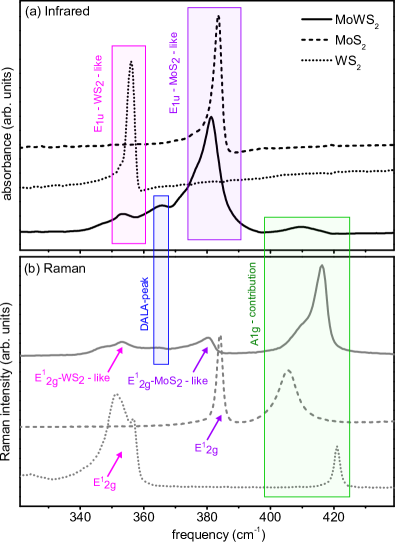
The absorbance spectrum of Mo0.5W0.5S2 is characterized by the presence of four distinct bands between 300 cm-1 and 450 cm-1. By comparing it with the spectra of WS2 and MoS2, the peaks at 350 cm-1 and 380 cm-1 can be assigned to the E1u-WS2-like and the E1u-MoS2-like modes respectively 26, 27. The larger bandwidth observed for the alloy peaks can be attributed to disorder-effects, which are less important in the binary crystals. It is interesting to notice that, although Mo and W atoms are present in the sample with the same percentage, the intensity of E1u-MoS2-like is far larger than that of E1u-WS2-like. We recall that the infrared phonon intensity is proportional to the square of the first derivative of the dipole moment with respect to the normal mode coordinates. The dipole moment is related to the Born effective charge tensor, i.e. the first derivative of the polarization per unit cell with respect to the atomic displacements. Based on the Density-Functional-Theory calculations reported in the literature 28, the Born charges (defined as one-third of the trace of the tensor in Cartesian coordinates) of Mo and W, for in-plane displacements, are in a 2:1 ratio, suggesting a four-times higher intensity of MoS2-like mode compared with WS2-like one. The less intense peak at 365 cm-1 between the two E1u phonons may correspond to the disorder-activated longitudinal acoustic (DALA) phonon mode 25, while the broad band at 410 cm-1 could be identified with the convoluted A1g modes from MoS2 and WS2 20. Interestingly, both the DALA and the A1g-like modes, whose symmetries are not compatible with the infrared selection rules, do not appear in the binary crystals but can be activated by disorder effects in the ternary compound.
2.2 Vibrational modes under high pressure
Room temperature transmission measurements on a Mo0.5W0.5S2 single crystal were performed in the 100600 cm-1 range, on increasing pressure from 0 to 31 GPa. The background intensity, , was measured with the DAC filled by the hydrostatic medium (CsI) only. The sample transmitted intensity, , was then collected once the crystal was loaded into the cell, to obtain the absorbance, , at each pressure. Interference fringes due to multiple reflections between the diamond surfaces through the hydrostatic medium were observed in spectra. The reduced number of oscillations and the frequency dependence of both the period and the amplitudeh of the oscillations prevent an effective subtraction in the spectra.
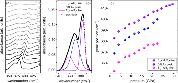
The absorbance spectra on increasing pressure in the 350430 cm-1 range, where the phonon contribution is dominant, are shown in Figure 2. Although the overall intensity of the peaks is reduced with respect to the out-of-cell measurements, a comparison with the spectra reported in Figure 1 allows us to identify the principal bands associated with E1u-WS2-like ( 350 cm-1), DALA ( 370 cm-1), and E1u-MoS2-like ( 380 cm-1) vibrational modes. In the cell measurements, the A1g-like contributions, visible at ambient conditions at 410 cm-1, are probably hindered by the interference fringes. Notice that, due to the alloyed nature of the compound, the relative intensity of the peaks may slightly vary depending on the measured point of the sample. In particular, disorder activated modes may be favoured in regions where the crystal order is reduced. By comparing Figures 1 and 2, the relative intensity of the DALA mode is higher in the first case than in the second one. Since that the investigated samples and the regions of the sample surface are different for in-cell- and out-of-cell-measurements, this effect can be ascribed to a different impact of configurational disorder.
As the pressure increases up to 31 GPa, the peak positions regularly shift toward higher frequencies, confirming the absence of structural transitions, as already suggested by Raman measurements 25. The peak intensities above 20 GPa undergo a progressive lowering until completely vanishing at 31 GPa.
2.3 Electronic properties at ambient conditions
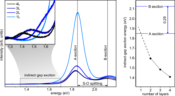
Thin Mo0.5W0.5S2 crystals, mechanically exfoliated on a SiO2-coated Si substrate, were analyzed through micro-Raman measurements to determine the number of layers (N) of each flake (see Supporting Information, SI). Photoluminescence (PL) measurements at ambient conditions were then performed to characterize the electronic properties of the sample as a function of N. PL spectra for mono-, bi-, tri- and four-layers samples are reported in Figure 3. The energy of the PL bands in the bulk sample is identical to that of the 4-layers sample, although the overall intensity is significantly lower. The spectrum of multi-layers samples exhibits three distinct bands: the one at lower energy ( 1.41.5 eV) corresponds to the exciton associated with the indirect-gap transition, the most intense one at 1.85 eV, is the A exciton, and the one at 2.1 eV is the B exciton, the latter two related to direct transitions 29. The energy difference between the peaks associated with A and B excitons corresponds to the spin-orbit splitting of the valence band of the crystal. In the mono-layer, the well-known transition from indirect to direct gap occurs, and the indirect transition band is no longer visible in the spectrum.
A comparison between the PL spectra of Mo0.5W0.5S2, MoS2, and WS2 (see SI) clearly shows that all the electronic features of the ternary compound lie at halfway between its basic constituents. In particular, in the bulk sample, we measured an indirect gap of 1.4 eV, a direct gap of 1.85 eV, and a spin-orbit splitting of 0.29 eV 29.
2.4 Electronic properties under high-pressure
To study the evolution of the electronic properties of Mo0.5W0.5S2 as a function of pressure, we analyzed the spectral weight in the far-infrared range at increasing pressure values. This quantity indeed accounts for the low-energy electronic transitions and, thus, allows to monitor a possible insurgence of the metallic regime.
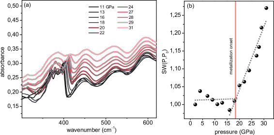
As shown in Figure 4(a), the spectra in the FIR region are almost superimposed up to 18 GPa. On further increasing pressure, the overall absorption intensity rises and the phonon peak intensity reduces. The first effect may arise from a rapid increase of the free electron density, due to the insurgence of a Drude band at zero frequency.
Indeed, as in most of semiconducting TMDs, in Mo0.5W0.5S2 the high pressure reasonably drives a progressive reduction of the band-gap responsible for the semiconductor-to-metal transition. Correspondingly, the intensity of the vibrational modes decreases since the optical response of the free electrons shields the phonon contribution in the FIR absorption.
To quantitatively characterize the metallization process, we define at each pressure the absorption spectral weight . A simple application of the Drude model proves that in the low-frequency limit, i.e. (where and is the Drude relaxation time), the absorbance is simply proportional to the square root of the DC conductivity and , . Since is proportional to the carrier density n, the last relation demonstrates that an increase in the FIR absorbance is directly related to an increase of n. Figure 4(b) reports the values of the normalized spectral weight up to 31 GPa, where GPa and the integration limits are =200 cm-1 and =700 cm-1. The integration is not performed over the 350450 cm-1 range where the phonon contribution is predominant. The normalized spectral weight, almost constant at low pressure, undergoes a significant increase around 20 GPa, associated to an increase of the charge carrier density n.
To identify the onset of the metallization process, two independent linear fits have been performed in the 220 GPa and the 1631 GPa regions, defining the metallization pressure, , as the ordinate of the crossing point between the fitting lines: GPa, see Figure 3(b).
The obtained results are well compatible with previous high-pressure measurements at room temperature on MoS2 and WS2, which have shown a metallic transition at 20 GPa for both samples 23, 24. Interestingly, in the Mo0.5W0.5S2 alloy the substitutional disorder of the crystal lattice, attested by the presence of the disorder-activated phonon peaks, does not strongly affect the electronic properties of the sample.
3 Experimental
Mo0.5W0.5S2, MoS2, and WS2 single crystals were provided by HQ-Graphene. All measurements were performed on fresh-cut, micrometric flakes, exfoliated from the macroscopic samples.
Room temperature infrared transmission measurements were performed at the beamline SMIS of the SOLEIL synchrotron both at ambient pressure (on all the samples) and over the 030 GPa range (only on Mo0.5W0.5S2).
In the DAC (orange), diamonds with a culet of 250 m2 were separated by a pre-indented stainless steel 50 m thick gasket, in which a hole of 125 m diameter was drilled. The exfoliated sample was positioned in the hole together with CsI as pressure transmitting medium 30 and a ruby chip, to measure the pressure through the ruby fluorescence technique 31.
The measured sample was 50 m2 in area and 2-3 m in thickness.
Measurements were performed using a Thermo Fisher iS50 interferometer equipped with a solid-substrate beamsplitter. Synchrotron edge radiation was employed as light source. Custom-made 15x Cassegrain objectives with a large working distance allowed to focus and then to collect the transmitted radiation, finally detected by a liquid-helium-cooled bolometer detector.
Raman and photoluminescence measurements at ambient conditions were collected on Mo0.5W0.5S2, MoS2 and WS2, using a Horiba LabRAM HR Evolution microspectrometer, with a 532 nm laser as light source. The radiation was focused on a 2 m2 spot on the sample by a 100x objective and collected by a CCD detector. Further details are provided in Ref. 32.
4 Conclusion
Transmission measurements were performed on a Mo0.5W0.5S2 single crystal in the far-infrared range. The spectrum collected at ambient conditions enabled the classification of the observed peaks in terms of the lattice vibrational modes, by comparison with the spectra of the binary constituents MoS2 and WS2. High-pressure measurements allowed us to study the evolution of both the lattice dynamics and the free carrier density up to 31 GPa. The absence of structural transitions, already suggested by Raman measurements, was confirmed, while an abrupt increase of the electron density was observed for the first time above 18 GPa. These results thus suggested the occurrence of an isostructural transition from a semiconducting to a metallic state, never investigated before in the literature. The observed effect is coherent with previous studies on the binary compounds MoS2 and WS2, which reported the onset of the metallization process at 19 GPa 23 and 22 GPa 24, respectively, without relevant changes in the lattice symmetries. The compatibility between the metallization pressures of Mo0.5W0.5S2 and its constituents suggests that substitutional disorder does not play a key role in the evolution of the electronic properties of the alloy under pressure.
References
- Yuan et al. 2016 Yuan, L.; Ge, J.; Peng, X.; Zhang, Q.; Wu, Z.; Jian, Y.; Xiong, X.; Yin, H.; Han, J. A reliable way of mechanical exfoliation of large scale two dimensional materials with high quality. AIP Adv. 2016, 6, 125201
- Manzeli et al. 2017 Manzeli, S.; Ovchinnikov, D.; Pasquier, D.; Yazyev, O. V.; Kis, A. 2D transition metal dichalcogenides. Nature Reviews Materials 2017, 2
- Peng et al. 2017 Peng, J.; Wu, J.; Li, X.; Zhou, Y.; Yu, Z.; Guo, Y.; Wu, J.; Lin, Y.; Li, Z.; Wu, X.; Wu, C.; Xie, Y. Very Large-Sized Transition Metal Dichalcogenides Monolayers from Fast Exfoliation by Manual Shaking. Journal of the American Chemical Society 2017, 139, 9019–9025
- Li et al. 2017 Li, X.; Tao, L.; Chen, Z.; Fang, H.; Li, X.; Wang, X.; Xu, J. B.; Zhu, H. Graphene and related two-dimensional materials: Structure-property relationships for electronics and optoelectronics. App. Phys. Rev. 2017, 4, 021306
- Wang et al. 2012 Wang, Q. H.; Kalantar-Zadeh, K.; Kis, A.; Coleman, J. N.; Strano, M. S. Electronics and optoelectronics of two-dimensional transition metal dichalcogenides. Nature Nanotechnology 2012, 7, 699–712
- Jariwala et al. 2014 Jariwala, D.; Sangwan, V. K.; Lauhon, L. J.; Marks, T. J.; Hersam, M. C. Emerging Device Applications for Semiconducting Two-Dimensional Transition Metal Dichalcogenides. ACS Nano 2014, 8, 1102–1120
- Yun et al. 2012 Yun, W. S.; Han, S. W.; Hong, I. G., S. C.and Kim; Lee, J. D. Thickness and strain effects on electronic structures of transition metal dichalcogenides: 2H-MX2 semiconductors (M = Mo, W; X = S, Se, Te). Phys. Rev. B 2012, 85, 033305
- Mak et al. 2010 Mak, K. F.; Lee, C.; Hone, J.; Shan, J.; Heinz, T. F. Atomically Thin MoS2: A New Direct-Gap Semiconductor. Phys. Rev. Lett. 2010, 105, 136805
- y. Zhang et al. 2013 y. Zhang et al., Direct observation of the transition from indirect to direct bandgap in atomically thin epitaxial MoSe2. Nat. Nanotechnol. 2013, 9, 111 EP –
- Xie 2015 Xie, L. M. Two-dimensional transition metal dichalcogenide alloys: preparation, characterization and applications. Nanoscale 2015, 7, 18392–18401
- Zhao et al. 2018 Zhao, Y.; Zhang, Z.; Ouyang, G. Band shift of 2D transition-metal dichalcogenide alloys: size and composition effects. Applied Physics A 2018, 124
- Sahoo et al. 2013 Sahoo, S.; Gaur, A. P. S.; Ahmadi, M.; Guinel, M. J.-F.; Katiyar, R. S. Temperature-Dependent Raman Studies and Thermal Conductivity of Few-Layer MoS2. The Journal of Physical Chemistry C 2013, 117, 9042–9047
- Chakraborty et al. 2012 Chakraborty, B.; Matte, H. S. S. R.; Sood, A. K.; Rao, C. N. R. Layer-dependent resonant Raman scattering of a few layer MoS2. Journal of Raman Spectroscopy 2012, 44, 92–96
- Mahatha et al. 2012 Mahatha, S. K.; Patel, K. D.; Menon, K. S. R. Electronic structure investigation of MoS2and MoSe2using angle-resolved photoemission spectroscopy andab initioband structure studies. Journal of Physics: Condensed Matter 2012, 24, 475504
- Ulstrup et al. 2017 Ulstrup, S.; Čabo, A. G. c. v. a. c.; Biswas, D.; Riley, J. M.; Dendzik, M.; Sanders, C. E.; Bianchi, M.; Cacho, C.; Matselyukh, D.; Chapman, R. T.; Springate, E.; King, P. D. C.; Miwa, J. A.; Hofmann, P. Spin and valley control of free carriers in single-layer . Phys. Rev. B 2017, 95, 041405
- Sekine et al. 1980 Sekine, T.; Nakashizu, T.; Toyoda, K.; Uchinokura, K.; Matsuura, E. Raman scattering in layered compound 2H-WS2. Solid State Communications 1980, 35, 371–373
- Wang et al. 2016 Wang, Z.; Liu, P.; Ito, Y.; Ning, S.; Tan, Y.; Fujita, T.; Hirata, A.; Chen, M. Chemical Vapor Deposition of Monolayer Mo1-xWxS2 Crystals with Tunable Band Gaps. Scientific Reports 2016, 6
- Kim et al. 2017 Kim, J.-S.; Ahmad, R.; Pandey, T.; Rai, A.; Feng, S.; Yang, J.; Lin, Z.; Terrones, M.; Banerjee, S. K.; Singh, A. K.; Akinwande, D.; Lin, J.-F. Towards band structure and band offset engineering of monolayer MoxW1-xS2 via Strain. 2D Materials 2017, 5, 015008
- Qiao et al. 2015 Qiao, X.-F.; Li, X.-L.; Zhang, X.; Shi, W.; Wu, J.-B.; Chen, T.; Tan, P.-H. Substrate-free layer-number identification of two-dimensional materials: A case of Mo0.5W0.5S2 alloy. Applied Physics Letters 2015, 106, 223102
- Zhang et al. 2015 Zhang, X.; Qiao, X.-F.; Shi, W.; Wu, J.-B.; Jiang, D.-S.; Tan, P.-H. Phonon and Raman scattering of two-dimensional transition metal dichalcogenides from monolayer, multilayer to bulk material. Chemical Society Reviews 2015, 44, 2757–2785
- Stellino 2020 Stellino, E. Pressure evolution of the optical phonons of MoTe2. Il Nuovo Cimento C 2020, 43, 1–8
- Yang et al. 2019 Yang, L.; Dai, L.; Li, H.; Hu, H.; Liu, K.; Pu, C.; Hong, M.; Liu, P. Pressure-induced metallization in MoSe2 under different pressure conditions. RSC Advances 2019, 9, 5794–5803
- Nayak et al. 2014 Nayak, A. P.; Bhattacharyya, S.; Zhu, J.; Liu, J.; Wu, X.; Pandey, T.; Jin, C.; Singh, A. K.; Akinwande, D.; Lin, J.-F. Pressure-induced semiconducting to metallic transition in multilayered molybdenum disulphide. Nature Communications 2014, 5
- Nayak et al. 2015 Nayak, A. P.; Yuan, Z.; Cao, B.; Liu, J.; Wu, J.; Moran, S. T.; Li, T.; Akinwande, D.; Jin, C.; Lin, J.-F. Pressure-Modulated Conductivity, Carrier Density, and Mobility of Multilayered Tungsten Disulfide. ACS Nano 2015, 9, 9117–9123
- Kim et al. 2016 Kim, J.-S.; Moran, S. T.; Nayak, A. P.; Pedahzur, S.; Ruiz, I.; Ponce, G.; Rodriguez, D.; Henny, J.; Liu, J.; Lin, J.-F.; Akinwande, D. High pressure Raman study of layered Mo0.5W0.5S2 ternary compound. 2D Materials 2016, 3, 025003
- O’Neal et al. 2016 O’Neal, K. R.; Cherian, J. G.; Zak, A.; Tenne, R.; Liu, Z.; Musfeldt, J. L. High Pressure Vibrational Properties of WS2 Nanotubes. Nano Letters 2016, 16, 993–999
- Guo et al. 2015 Guo, X.; Chen, H.; Wen, X.; Zheng, J. Electron-phonon interactions in MoS2 probed with ultrafast two-dimensional visible/far-infrared spectroscopy. The Journal of Chemical Physics 2015, 142, 212447
- Pike et al. 2017 Pike, N. A.; Van Troeye, B.; Dewandre, A.; Petretto, G.; Gonze, X.; Rignanese, G.-M.; Verstraete, M. J. Origin of the counterintuitive dynamic charge in the transition metal dichalcogenides. Phys. Rev. B 2017, 95, 201106
- Chen et al. 2013 Chen, Y.; Xi, J.; Dumcenco, D. O.; Liu, Z.; Suenaga, K.; Wang, D.; Shuai, Z.; Huang, Y.-S.; Xie, L. Tunable Band Gap Photoluminescence from Atomically Thin Transition-Metal Dichalcogenide Alloys. ACS Nano 2013, 7, 4610–4616
- Celeste et al. 2019 Celeste, A.; Borondics, F.; Capitani, F. Hydrostaticity of pressure-transmitting media for high pressure infrared spectroscopy. High Pressure Research 2019, 39, 608–618
- Chijioke et al. 2005 Chijioke, A. D.; Nellis, W. J.; Soldatov, A.; Silvera, I. F. The ruby pressure standard to 150GPa. Journal of Applied Physics 2005, 98, 114905
- Caramazza et al. 2018 Caramazza, S.; Collina, A.; Stellino, E.; Ripanti, F.; Dore, P.; Postorino, P. First-and second-order Raman scattering from MoTe 2 single crystal. The European Physical Journal B 2018, 91, 1–7