Ferroelectric HfO2 Memory Transistors with High- Interfacial Layer and Write Endurance Exceeding Cycles
Abstract
We demonstrate ferroelectric (FE) memory transistors on a crystalline silicon channel with endurance exceeding cycles. The ferroelectric transistors (FeFETs) incorporate a high- interfacial layer (IL) of thermally grown silicon nitride (SiNx) and a thin 4.5 nm layer of Zr-doped FE-HfO2 on a 30 nm SOI channel. The device shows a 1V memory window in a DC sweep of just 2.5V, and can be programmed and erased with voltage pulses of 3V at a pulse width of 250 ns. The device also shows very good retention behavior. These results indicate that appropriate engineering of the IL layer could substantially improve FeFET device performance and reliability.
I Introduction
Despite the fact that there has been much rekindled interest in ferroelectrics-based nonvolatile memories due to the discovery of CMOS-compatible doped HfO2 materials [1, 2, 3, 4, 5, 6, 7, 8], one of the key roadblocks facing the development of FeFETs specifically is endurance. It has been shown, for thicker 5-6 nm FE oxides, that bulk charge-trapping and interfacial layer breakdown (due to the large coercive fields associated with ferroelectric HfO2, and therefore, the larger write voltages needed to program FeFETs with thicker FE oxides) tend to cause premature device failure [9, 10], with many groups reporting typical endurance metrics of - cycles [11, 12, 13, 14]. For thinner FE oxides 5nm in physical thickness, hot electron-induced hole damage and channel/oxide interface degradation tend to be the key agents limiting device endurance [15].
Proposals to extend the cycling lifetime of FeFETs include interfacial oxide engineering, gate workfunction engineering, modulating the material properties of the FE layer itself, and many others [16, 17, 18, 19, 20, 21]. In this work, we combine a high- interfacial layer (IL) together with a thin FE film (4.5 nm). This is motivated by the previous observation by many authors (such as [5]) that the endurance cycling is mostly limited by IL breakdown. In fact, in a metal-FE-metal capacitor configuration, cycling endurance metrics exceeding 1010 are routinely observed [2]. In a recent report, Abhishek et. al. circumvented the interfacial layer breakdown problem by fabricating a bottom-gate, channel last transistor, where an oxide semiconductor channel was grown directly on the FE material, thus achieving an endurance exceeding 1012 cycles [22]. Similarly, Kim et. al. recently reported on the fabrication of vertical 3D NAND FE thin film transistors utilizing indium zinc oxide as the semiconductor channel, showing a cycling endurance of up to [23]. Nonetheless, when crystalline Si is used as the channel material, as is required for high performance memory, formation of an IL is inevitable, and therefore endurance still remains a critical challenge to be addressed.
In the context of IL breakdown, it is known that ‘time-to-breakdown’ has an exponential relationship to the applied electric field in the interfacial layer [24]. In other words, a mild decrease in the electric field could still lead to a substantial increase in the ‘time-to-breakdown’, and therefore could slow the generation of traps that eventually counteract the FE hysteresis. For the same charge density, a high- IL reduces the electric field by the ratio of its permittivity to that of SiO2. Our choice of high- IL is thermal nitridation of chemically formed silicon oxide. This provides a simple way to achieve an IL with a permittivity . Thermally grown silicon nitride also has a comparable breakdown field to SiO2[25]. A thin 4.5 nm of FE HZO is chosen to suppress the effects of bulk charge trapping [15] and demonstrates the thickness scalability of FE HZO. We show that this combination substantially improves the device performance. In a DC sweep, almost a 1V memory window can be achieved with just V. More importantly, with bipolar stress pulsing at V, 250 ns, the endurance exceeds 1010 cycles on silicon.
II Experiment and EOT Comparison
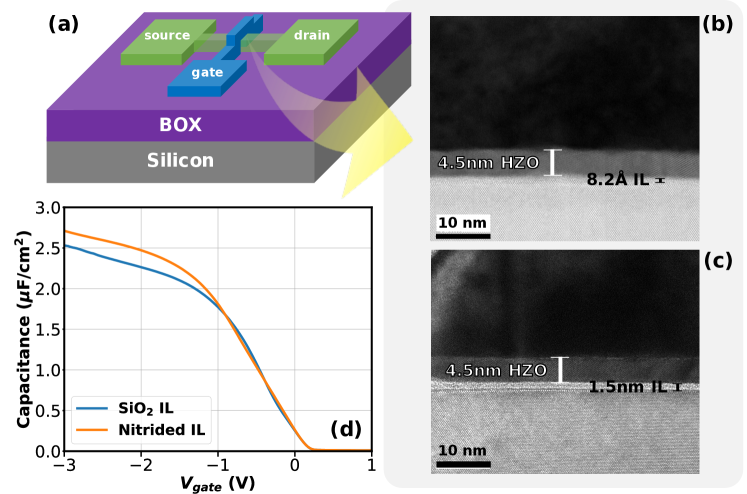
The structure of the FeFET device characterized in this work is shown in Fig. 1(a), and TEMs to compare its gate stack incorporating a nitrided IL against that of a baseline device with an SiO2 IL (characterized in previous work [15]) are shown in Fig. 1(c) and Fig. 1(b), respectively. The process flow to realize the FeFET is described in [11], with the IL formation step involving thermal nitridation of the SOI substrate at 850 C in NH3 ambient rather than a self-terminated chemical growth of SiO2. As confirmed through TEM, the FE oxide thickness of both the control SiO2 FeFET and the FeFET with a nitrided IL are the same (roughly 4.5 nm after 45 cycles of deposition). The IL thicknesses of the SiO2 IL and nitrided IL are 8 and 1.5 nm, respectively.
Fig. 1(d) compares the CV of the baseline FeFET with a SiO2 IL to the CV of the FeFET with a nitrided IL. Though the physical thickness of the gate stack of the latter is larger, its capacitance is also larger. Using Synopsys TCAD, we have estimated the net EOT of the nitrided sample to be roughly 1 smaller than the baseline sample, based upon the accumulation capacitances. This allows us to make an estimate for the effective of the IL as follows:
where and indicate the values of the nitrided IL and SiO2 IL respectively; and indicate the physical thicknesses of the nitrided IL and SiO2 IL respectively; and is the simulated EOT difference between the two ILs. This calculation indicates the IL is nearly all Si3N4. Therefore, we expect to reduce the electric field in the IL layer by two times, which will ultimately result in a substantial increase in the time to breakdown.
III Results and Discussion
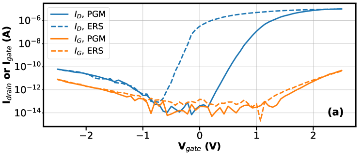
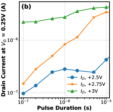
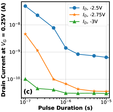
We first investigate the DC hysteresis of the fabricated device with a nitrided IL. Fig. 2(a) shows results of a doubly swept curve. Nearly a 1V memory window can be achieved with just V sweep. We note that, compared to published literature, this is quite a low voltage requirement. For example, our baseline devices as reported in [15] do not demonstrate any appreciable memory window at V. Nonetheless it is also well known that the time to switch a given amount of polarization depends strongly on the applied voltage. Therefore, although the DC sweep is a good way of visualizing the hysteresis, it is important to also probe the high-speed switching behavior. Fig. 2(b) and (c) show measured current at a read voltage of V as a function of pulse width. We define the high current/low state as the ERS state, and the low current/high state as the PGM state. Unsurprisingly, we observe a strong dependence of the current with the applied voltage. Below 1 s, 2.5V is not good enough to provide the current level we see in the DC hysteresis. As the voltage amplitude increases, the current increases, signifying switching of a larger amount of polarization. At V, the current approaches the level seen in DC hysteresis, even for a pulse width of 100 ns. Similarly, for the PGM state, V brings the current level down to almost the level seen in the DC hysteresis at a pulse width of 250 ns. The asymmetry between PGM and ERS states is expected – accumulation of a thin SOI body requires a much larger voltage drop across the semiconductor, as discussed in previous reports[4]. Therefore, for a reasonably fast and symmetric operation, we choose a pulse width of 250 ns and a gate voltage of V for endurance cycling.
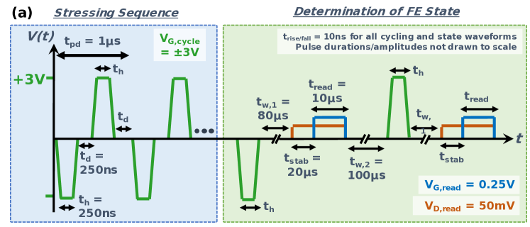
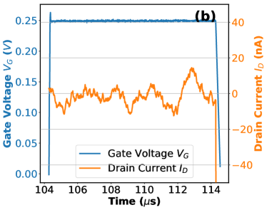
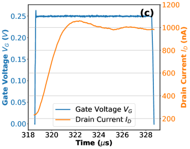
In many studies, the endurance is quantified by measuring after a certain number of bipolar stress pulses. The determination requires one to perform sweeps over a small voltage range, which typically takes second to complete. On the other hand, the importance of fast reading has recently been discussed (e.g. [22]). It is known from charge pumping experiments (as discussed in [26, 15]) that beyond several s, charge trapping/de-trapping starts to manifest. These effects could in principle be quite complex, and could arise from the interplay between traps with varying time constants. Therefore, while slow sweeps to determine could provide important insights into trap assisted phenomena, they are also expected to artificially affect the actual currents that will be observed in a real application where the device is read quickly. Due to these considerations, we adopt fast reading of the device to determine its state. The complete endurance testing protocol is detailed in Fig. 3(a). During the stressing phase of the endurance test, bipolar voltage pulses of V, 250 ns are applied at the gate of the FeFET, with a 250 ns delay between sequential pulses to achieve a stressing period of 1 s total in duration. Periodically, a state determination test is conducted to evaluate the margin between the PGM and ERS states. For this, a 10 s read pulse is applied at the gate of the FeFET (after either the ERS or PGM pulse), after ramping and stabilizing the drain voltage to 50 mV (see Fig. 3(a), right panel). The averaged current value during this 10 s reading period is determined to be the read current. Figs. 3(b) and (c) show the readout current during the 10 s reading period for the high (PGM) and low (ERS) states, respectively. In both cases, the current saturates well within the READ duration of 10 s.
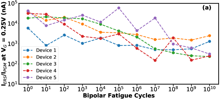
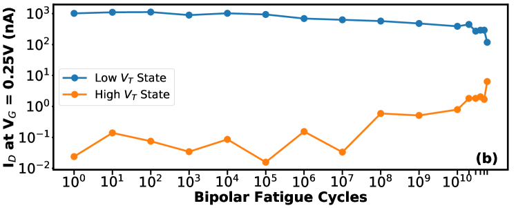
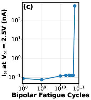
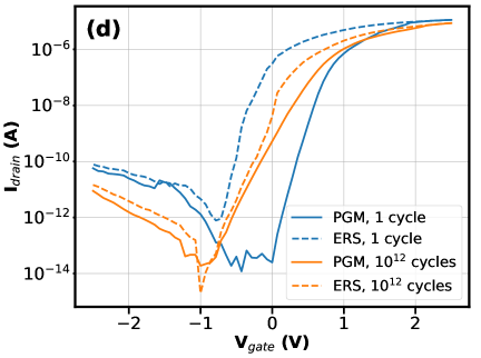
Fig. 4(a) shows the results of endurance testing across different devices, proving that the devices with a nitrided IL can be reliably cycled to . The data is plotted as vs. fatigue cycles for ease of comparison. The exact current levels are shown for a device in Fig. 4(b). First, we note that the high and low current levels are very similar to those measured from a DC sweep. This indicates that the device is switched properly with the PGM/ERS pulses. Interestingly, the device does not show any rapid degradation after cycles, as reported in most studies. Rather, the high current level shows a slow degradation. The envelope of the low current similarly shows a slow degradation (increase); yet the separation of the current levels retains a margin of until cycles. Beyond that point, a sudden breakdown is observed. Notably, this sudden breakdown is correlated with the gate leakage through the device shooting up several orders of magnitude, as shown in Fig. 4(c), indicating that the gate oxide itself breaks down close to cycles. We note that, there are devices that does not experience such a breakdown. For example, Fig. 4(d) shows DC sweep from an exemplary device cycled to . The anti-clockwise Hysteresis is still clearly visible. This should compared with previous studies where total reversal of handedness of Hysteresis happens after just 104-105 cycles. This also shows that the Ferroelectric itself remains quite robust even after one trillion cycles.
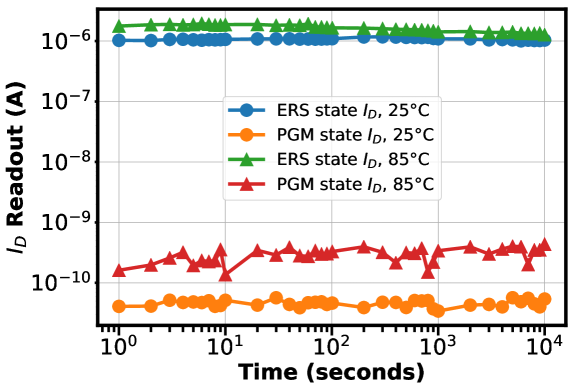
Finally, we present the retention behavior. As seen in Fig. 5, the retention looks unaffected for a testing duration of seconds for both the PGM and ERS states. The retention looks robust at both 25°C and 85°C. Thus despite relatively lower voltage operation and very large endurance, there is no discernible effect on the retention behavior.
IV Conclusion
In conclusion, we have demonstrated a FeFET memory device with an engineered high- IL that shows larger than 1010 endurance cycles at a relatively small PGM/ERS voltage of V and pulse width of 250 ns. Endurance measured on multiple devices show robust and repeatable behavior over 1010 endurance cycles. We have identified total oxide breakdown as the main limiting factor as opposed to defect (interface and bulk) induced clock-wise Hysteresis that has been reported by many previous studies. Understanding charge injection during the endurance test and optimizing to reduce the total oxide breakdown could increase the endurance over 1012 cycles, as our data shows that the FE film remains robust even beyond that cycling number. Additional optimization of the IL and FE layers could allow for further reduction in the operating voltage to below 2V, while maintaining and/or even enhancing the endurance behavior. One potential drawback of using such a high- IL could be a reduction in mobility. However, somewhat reduced mobility could still be tolerable as these devices are not expected to compete with the gate-delay of logic devices.
References
- [1] A. J. Tan, L. C. Wang, Y. H. Liao, J. H. Bae, C. Hu, and S. Salahuddin, “Reliability of ferroelectric hfo2-based memories: From mos capacitor to fefet,” in 2020 Device Research Conference (DRC), 2020. doi: 10.1109/DRC50226.2020.9135148 pp. 1–2.
- [2] M. Pešić, U. Schroeder, S. Slesazeck, and T. Mikolajick, “Comparative study of reliability of ferroelectric and anti-ferroelectric memories,” IEEE Transactions on Device and Materials Reliability, vol. 18, no. 2, pp. 154–162, 2018. doi: 10.1109/TDMR.2018.2829112
- [3] H. Mulaosmanovic, E. T. Breyer, T. Mikolajick, and S. Slesazeck, “Recovery of cycling endurance failure in ferroelectric fets by self-heating,” IEEE Electron Device Letters, vol. 40, no. 2, pp. 216–219, 2019. doi: 10.1109/LED.2018.2889412
- [4] J. H. Bae, D. Kwon, N. Jeon, S. Cheema, A. J. Tan, C. Hu, and S. Salahuddin, “Highly scaled, high endurance, omega-gate, nanowire ferroelectric fet memory transistors,” IEEE Electron Device Letters, vol. 41, no. 11, pp. 1637–1640, 2020. doi: 10.1109/LED.2020.3028339
- [5] K. Chatterjee, S. Kim, G. Karbasian, A. J. Tan, A. K. Yadav, A. I. Khan, C. Hu, and S. Salahuddin, “Self-aligned, gate last, fdsoi, ferroelectric gate memory device with 5.5-nm hf0.8zr0.2o2, high endurance and breakdown recovery,” IEEE Electron Device Letters, vol. 38, no. 10, pp. 1379–1382, 2017. doi: 10.1109/LED.2017.2748992
- [6] H. Liu, C. Wang, G. Han, J. Li, Y. Peng, Y. Liu, X. Wang, N. Zhong, C. Duan, X. Wang, N. Xu, T. K. Liu, and Y. Hao, “Zro2 ferroelectric fet for non-volatile memory application,” IEEE Electron Device Letters, vol. 40, no. 9, pp. 1419–1422, 2019. doi: 10.1109/LED.2019.2930458
- [7] K. Lee, J. Bae, S. Kim, J. Lee, B. Park, and D. Kwon, “Ferroelectric-gate field-effect transistor memory with recessed channel,” IEEE Electron Device Letters, vol. 41, no. 8, pp. 1201–1204, 2020. doi: 10.1109/LED.2020.3001129
- [8] A. J. Tan, Z. Zhu, H. S. Choe, C. Hu, S. Salahuddin, and A. Yoon, “Ferroelectric si-doped hfo2 capacitors for next-generation memories,” in 2019 International Symposium on VLSI Technology, Systems and Application (VLSI-TSA), 2019. doi: 10.1109/VLSI-TSA.2019.8804657 pp. 1–2.
- [9] E. Yurchuk, J. Müller, S. Müller, J. Paul, M. Pešić, R. van Bentum, U. Schroeder, and T. Mikolajick, “Charge-trapping phenomena in hfo2-based fefet-type nonvolatile memories,” IEEE Transactions on Electron Devices, vol. 63, no. 9, pp. 3501–3507, 2016. doi: 10.1109/TED.2016.2588439
- [10] H. Mulaosmanovic, E. T. Breyer, T. Mikolajick, and S. Slesazeck, “Ferroelectric fets with 20-nm-thick hfo2 layer for large memory window and high performance,” IEEE Transactions on Electron Devices, vol. 66, no. 9, pp. 3828–3833, 2019. doi: 10.1109/TED.2019.2930749
- [11] A. J. Tan, K. Chatterjee, J. Zhou, D. Kwon, Y. Liao, S. Cheema, C. Hu, and S. Salahuddin, “Experimental demonstration of a ferroelectric hfo2-based content addressable memory cell,” IEEE Electron Device Letters, vol. 41, no. 2, pp. 240–243, 2020. doi: 10.1109/LED.2019.2963300
- [12] K. . Chen, H. . Chen, C. . Liao, G. . Siang, C. Lo, M. . Liao, K. . Li, S. T. Chang, and M. H. Lee, “Non-volatile ferroelectric fets using 5-nm hf0.5zr0.5o2 with high data retention and read endurance for 1t memory applications,” IEEE Electron Device Letters, vol. 40, no. 3, pp. 399–402, 2019. doi: 10.1109/LED.2019.2896231
- [13] T. Ali, P. Polakowski, S. Riedel, T. Büttner, T. Kämpfe, M. Rudolph, B. Pätzold, K. Seidel, D. Löhr, R. Hoffmann, M. Czernohorsky, K. Kühnel, P. Steinke, J. Calvo, K. Zimmermann, and J. Müller, “High endurance ferroelectric hafnium oxide-based fefet memory without retention penalty,” IEEE Transactions on Electron Devices, vol. 65, no. 9, pp. 3769–3774, 2018. doi: 10.1109/TED.2018.2856818
- [14] K. Florent, S. Lavizzari, L. Di Piazza, M. Popovici, E. Vecchio, G. Potoms, G. Groeseneken, and J. Van IHoudt, “First demonstration of vertically stacked ferroelectric al doped hfo 2 devices for nand applications,” in 2017 Symposium on VLSI Technology. IEEE, 2017, pp. T158–T159.
- [15] A. J. Tan, M. Pešic, L. Larcher, Y. H. Liao, L. C. Wang, J. H. Bae, C. Hu, and S. Salahuddin, “Hot electrons as the dominant source of degradation for sub-5nm hzo fefets,” in 2020 IEEE Symposium on VLSI Technology, 2020. doi: 10.1109/VLSITechnology18217.2020.9265067 pp. 1–2.
- [16] A. J. Tan, A. K. Yadav, K. Chatterjee, D. Kwon, S. Kim, C. Hu, and S. Salahuddin, “A nitrided interfacial oxide for interface state improvement in hafnium zirconium oxide-based ferroelectric transistor technology,” IEEE Electron Device Letters, vol. 39, no. 1, pp. 95–98, 2018. doi: 10.1109/LED.2017.2772791
- [17] S. Deng, Z. Liu, X. Li, T. P. Ma, and K. Ni, “Guidelines for ferroelectric fet reliability optimization: Charge matching,” IEEE Electron Device Letters, vol. 41, no. 9, pp. 1348–1351, 2020. doi: 10.1109/LED.2020.3011037
- [18] K. Ni, P. Sharma, J. Zhang, M. Jerry, J. A. Smith, K. Tapily, R. Clark, S. Mahapatra, and S. Datta, “Critical role of interlayer in hf0.5zr0.5o2 ferroelectric fet nonvolatile memory performance,” IEEE Transactions on Electron Devices, vol. 65, no. 6, pp. 2461–2469, 2018. doi: 10.1109/TED.2018.2829122
- [19] A. G. Chernikova, M. G. Kozodaev, D. V. Negrov, E. V. Korostylev, M. H. Park, U. Schroeder, C. S. Hwang, and A. M. Markeev, “Improved ferroelectric switching endurance of la-doped hf0.5zr0.5o2 thin films,” ACS Applied Materials & Interfaces, vol. 10, no. 3, pp. 2701–2708, 2018. doi: 10.1021/acsami.7b15110 PMID: 29282976. [Online]. Available: https://doi.org/10.1021/acsami.7b15110
- [20] R. Cao, B. Song, D. Shang, Y. Yang, Q. Luo, S. Wu, Y. Li, Y. Wang, H. Lv, Q. Liu, and M. Liu, “Improvement of endurance in hzo-based ferroelectric capacitor using ru electrode,” IEEE Electron Device Letters, vol. 40, no. 11, pp. 1744–1747, 2019. doi: 10.1109/LED.2019.2944960
- [21] S. Oh, J. Song, I. K. Yoo, and H. Hwang, “Improved endurance of hfo2-based metal- ferroelectric-insulator-silicon structure by high-pressure hydrogen annealing,” IEEE Electron Device Letters, vol. 40, no. 7, pp. 1092–1095, 2019. doi: 10.1109/LED.2019.2914700
- [22] A. A. Sharma, B. Doyle, H. J. Yoo, I.-C. Tung, J. Kavalieros, M. V. Metz, M. Reshotko, P. Majhi, T. Brown-Heft, Y.-J. Chen, and V. H. Le, “High speed memory operation in channel-last, back-gated ferroelectric transistors,” in 2020 International Electron Devices Meeting. IEEE, 2020.
- [23] M.-K. Kim, I.-J. Kim, and J.-S. Lee, “Cmos-compatible ferroelectric nand flash memory for high-density, low-power, and high-speed three-dimensional memory,” Science Advances, vol. 7, no. 3, 2021. doi: 10.1126/sciadv.abe1341. [Online]. Available: https://advances.sciencemag.org/content/7/3/eabe1341
- [24] K. F. Schuegraf and C. Hu, “Hole injection sio/sub 2/breakdown model for very low voltage lifetime extrapolation,” IEEE transactions on electron devices, vol. 41, no. 5, pp. 761–767, 1994.
- [25] T. Ito, T. Nozaki, H. Arakawa, and M. Shinoda, “Thermally grown silicon nitride films for high-performance mns devices,” Applied Physics Letters, vol. 32, no. 5, pp. 330–331, 1978.
- [26] M. Pesic, A. Padovani, S. Slcsazeck, T. Mikolajick, and L. Larcher, “Deconvoluting charge trapping and nucleation interplay in fefets: Kinetics and reliability,” in 2018 IEEE International Electron Devices Meeting (IEDM), 2018. doi: 10.1109/IEDM.2018.8614492 pp. 25.1.1–25.1.4.