Interlayer excitonic spectra of vertically stacked MoSe2/WSe2 heterobilayers
Abstract
The optical spectra of vertically stacked MoSe2/WSe2 heterostructures contain additional ’interlayer’ excitonic peaks that are absent in the individual monolayer materials and exhibit a significant spatial charge separation in out-of-plane direction. Extending on a previous study, we used a many-body perturbation theory approach to simulate and analyse the excitonic spectra of MoSe2/WSe2 heterobilayers with three stacking orders, considering both momentum-direct and momentum-indirect excitons. We find that the small oscillator strengths and corresponding optical responses of the interlayer excitons are significantly stacking-dependent and give rise to high radiative lifetimes in the range of 5-200 ns (at T=4 K) for the ’bright’ interlayer excitons. Solving the finite-momentum Bethe-Salpeter Equation, we predict that the lowest-energy excitation should be an indirect exciton over the fundamental indirect band gap (KQ), with a binding energy of 220 meV. However, in agreement with recent magneto-optics experiments and previous theoretical studies, our simulations of the effective excitonic Landé g-factors suggest that the low-energy momentum-indirect excitons are not experimentally observed for MoSe2/WSe2 heterostructures. We further reveal the existence of ’interlayer’ C excitons with significant exciton binding energies and optical oscillator strengths, which are analogous to the prominent band nesting excitons in mono- and few-layer transition-metal dichalcogenides.
I Introduction
The experimental realization of Graphene in 2004 (graphene-2004, ; novoselov-2005, ) inspired an ongoing search for novel energetically stable quasi-two-dimensional materials and a detailed experimental and theoretical study of the influence of their reduced dimensionality. Recent theoretical reports based on high-throughput screening and machine-learning methods suggest that several thousand exfoliable, and largely unsynthesized, materials exist new-materials-1 ; new-materials-2 , offering a rich pool of materials with diverse physical properties.
A particularly interesting and well-researched family of novel two-dimensional materials are the transition metal dichalcogenides (TMDC) of molybdenum and tungsten with the structural formula (with =Mo,W and =S,Se,Te). These materials have been well known in their bulk phases, where they are indirect semiconductors with band gaps in the range of 0.8-1.3 eV and assume a layered structure with hexagonal symmetry. Analogously to graphite, the atoms within the layers are bonded covalently, while the layers are bound together mainly through non-covalent interactions. Interestingly, it had been realized early that this interlayer interaction, albeit weak compared to the covalent intralayer bonds, has a significant effect on the electronic and optical properties of molybdenum and tungsten TMDCs: the fundamental band gap is indirect in bulk and few-layer samples and increases with decreasing thickness due to quantum confinement effects and the attenuation of interlayer-coupling induced splittings of the valence and conduction band edges. In the absence of interlayer coupling effects in the monolayer limit, the band gap is direct, causing a strong enhancement of photoluminescence quantum yield for decreasing material thickness (mak-2010, ; splendiani-2010, ; MoSe2WSe2MoS2-PL, ; WS2-PL, ; MoS2-tunable-PL, ; scheuschner-2014, ).
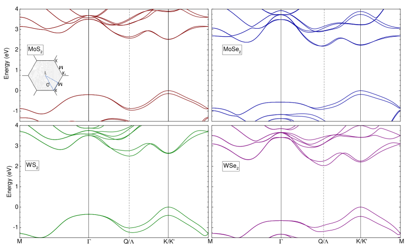
At the same time, the reduced dimensionality and highly non-local dielectric screening of Coulomb interaction give rise to rather large exciton binding energies on the order of 0.3-0.6 eV for monolayer molybdenum and tungsten TMDCs MoS2-exciton-binding-2 ; WSe2-binding1 ; ugeda-MoSe2-excitons ; WS2-binding1 ; MoS2-WS2-exciton-binding-hill ; WSe2-binding2 ; MoS2-WS2-exciton-binding-rigosi ; chernikov-review ; Goryca2019 despite the exciton wavefunctions to be rather expanded, with typical Bohr radii on the order of 2 nm Goryca2019 ; qiu-2013 ; exciton-paper . Further, the electronic band structures of molybdenum and tungsten disulfides, -selenides and -tellurites show several local conduction and valence band extrema of similar energies, see Figure 1. This gives rise to a rich excitonic spectrum in mono- and few-layer TMDCs, dominated by ’A’ excitons originating from the direct band gaps and, in few-layer materials, ’I’ transistions associated with the indirect fundamental band gap. Interestingly, strongly bound ’C’ excitons appear at higher energies, between 2.0 and 3.0 eV, depending on the material, arising from a band nesting between valence and conduction band edges and an associated high-joint density at special points in the Brillouin zone carvalho-band-nesting ; qiu-2013 ; exciton-paper .
The strong spin-orbit interaction introduced by the heavy transition metal atoms further leads to a prominent splitting of the valence band maximum at the corners of the two-dimensional hexagonal Brillouin zones, allowing to exploit the circular dichroism for valley selective optical excitations with circularly polarized light. These findings inspired the use of mono- and few-layer TMDCs for a range of novel applications of TMDCs in novel thin and flexible optoelectronic devices, such as photodiodesled1 ; led2 , photodetectorsphotodetector1 or single-photon emitterssingle-photon2 ; single-photon3 ; single-photon4 ; single-photon5 , and for a combination of spin- and valleytronicsspinvalley-1 ; spinvalley-2 .
A possible way to further tailor the electronic and optical properties of TMDCs is the combination of different TMDCs to form vertically stacked heterostructures. Here, the non-covalent interlayer interaction in principle allows for atomically sharp and essentially strain-free interfaces even for lattice-mismatched materials; particularly interesting compared to conventional heterostructures formed of 3D bulk materials, where interfacial defects can have a significant effect on the material properties. Recently, the combination of Mo and W based TMDCs arose substantial interest: for MoS2/WS2MoS2WS2-1 , MoS2/WSe2MoS2-WSe2-1 ; kunstmann-interlayer-excitons ; Karni-Mos2Wse2 , MoSe2/WSe2WSe2MoSe2-2 ; WSe2MoSe2-3 ; Nayak-MoSe2WSe2-twist ; moire-MoSe2WSe2 ; geim-MoSe2WSe2 and MoSe2/WS2MoSe2WS2-1 ; MoSe2WS2-2 heterostructures, experimental observations indicate the presence of additional photoluminescence (PL) signals from excitations with long lifetimes of 1-100 ns WSe2MoSe2-2 ; miller-MoSe2WSe2 , which are absent in the PL spectra of the individual monolayer materials.
The detailed origin of these transitions is still not entirely clear and might vary with the material combination and experimentally studied samples. Theoretical studies predict that the aforementioned heterostructures form type-II heterostructures with the valence and conduction band edges of the composite materials being localized in different layers kang-offsets . For this reason, a reasonable and popular explanation of the observed signals is the attribution to interlayer excitons with a distinct spatial separation of the bound electrons and holes, an interesting concept for application in photovoltaics based on such heterostructures MoSe2-WSe2-photovoltaics . These arguments are based on the assumption that the interlayer coupling between the individual materials is small enough that the electronic properties of the individual materials are largely unaffected. However, it is known from the TMDC homo-multilayer materials, such as bilayer MoS2, that the (rather weak) hybridization between S or Se states in the different layers causes an interlayer-induced band splitting and a layer-number dependent direct-to-indirect band gap transition. At the same time, these additional signals are somewhat reminiscent of the ’I’ transitions in TMDC homo-bilayers and might indicate phonon- or defect-assisted emission over an indirect band gap.
Due to the rather complex nature of the TMDC band structures with several conduction band and valence band valleys with similar energies and additional spin-orbit and interlayer coupling effects, a clear identification of the origin of these peaks is non-trivial and strongly depends on a comparison of experimental data with theoretical predictions of the electronic bandstructure, exciton binding energies and the orbital composition of relevant bands. For instance, Kunstmann et al. used a correlation of the PL spectra in MoS2/WSe2 heterostructures with various twist angles with the respective DFT band gaps to attribute the prominent ’interlayer’ PL peak at around 1.6 eV to a momentum-indirect exciton, with the bound electron and hole being located at the K point and the center of the hexagonal Brillouin zone, respectively kunstmann-interlayer-excitons . Additionally, recent PL measurements on BN-encapsulated MoS2/WSe2 heterostructures with small twist angle suggest the presence of an additional excitonic signal at an energy of about 1 eV, well below the fundamental band gap of the heterostructure, with a significant Stark shift indicating a strong vertical separation of the electron-hole pair by about 6 Å. Based on theoretical simulations, this infrared peak was attributed to a transition between the global valence band maximum at the K point of the WSe2 layer and the global conduction band minimum at the K-point of the MoS2 layer Karni-Mos2Wse2 .
For nearly lattice-matched MoSe2/WSe2 heterostructures, low-temperature experiments revealed that the prominent interlayer peak consists of a doublet of two separate contributions with a small energy difference of 25 meV. Due to the aforementioned complexities of the electronic band structure, the exact origin or these peaks is still a matter of debate. Depending on the experimental evidence and insight from theoretical calculations, the PL signals were attributed to (i) a mix of momentum direct () and momentum-indirect () interlayer excitons, evidenced by the different temperature behaviors of the PL peak lifetimes WSe2MoSe2-2 ; miller-MoSe2WSe2 , (ii) to a pair of momentum-indirect excitons, with an energy separation due to the spin-orbit splitting of the conduction band valley at the point, evidenced by the observed opposite circular polarization hanbicki-MoSe2WSe2 , (iii) a singlet-triplet pair of neutral, momentum-direct, excitons at the K and K’ points, evidenced by recent measurements of the interlayer exciton photoluminescence under application of external magnetic fields Ciarrocchi-nature-MoSe2WSe2 ; Wang2020 ; Delhomme2020 ; foerg2020moire , and (iv) a pair of spatially indirect neutral exciton and spatially indirect negatively charged trion, evidenced by an observed constant relative intensity of the two PL signals at low temperature geim-MoSe2WSe2 , but somewhat contradicted by the circular polarization response reported by other authors. For structurally similar MoS2/WS2 hetero-bilayers, experimental reports suggest the existence of three interlayer exciton peaks, which were attributed to , , and transitions based on a combination of optical measurements and DFT+BSE Okada-MoS2WS2 .
An alternative explanation for the origin of the observed interlayer exciton peak structure is offered by the effects of the intrinsic (albeit small) lattice mismatch and small deviations in relative twist angles from the symmetric stacking orders in studied samples, giving rise to long-period moiré superlattices and corresponding moiré potentials, which might activate otherwise optically forbidden spin-flip transitions Ciarrocchi-nature-MoSe2WSe2 and allow for a moiré trapping and localization of excitonic states in the minima of the moiré superlattice potential Seyler-MoSe2WSe2-moire , of significant potential interest for manipulation of excitons in van-der-Waals heterostructures. Additionally, the differences in local stacking order have been shown to affect the interlayer exciton binding energies, oscillator strengths, and optical selection rules gillen-interlayer . Based on magneto-luminescence experiments, a recent study suggested that the interlayer PL peaks in twisted MoSe2/WSe2 heterobi- and trilayer systems in R registry arise from moiré potential modulated momentum-direct and phonon-assisted momentum-indirect interlayer exciton emissions, respectively Hoegele-MoSe2WSe2-moire .
On the theoretical side, accurate ab initio investigations of the excitonic spectra of van-der-Waals heterostructures are limited to rather small and symmetric systems due to the delicate interplay of quasiparticle bandstructure, effects from interlayer interaction and spin-orbit coupling and (computationally expensive) Coulomb interaction between electrons and holes. Despite these constraints, a number of studies using various methods have been reported recently, typically focussing on the properties of momentum-direct interlayer excitons palumno-2015 ; lantini-2017 ; gillen-interlayer ; wirtz-interlayer ; Okada-MoS2WS2 ; deilmann-MoS2WS2 ; interlayer-moire-bse and trions deilmann-MoS2WS2 . On the other hand, to the best of our knowledge, there is no reliable theoretical data so far on the binding energies and wavefunctions of momentum-indirect excitons, which could significantly contribute to the detailed understanding of the experimental observations of interlayer exciton emissions. Another question that has not yet been addressed concerns the structure of the absorption above the intralayer band gaps, which is dominated by ’C’ excitons with high binding energy and significant interlayer delocalization in TMDC homo-single- and -fewlayer systems exciton-paper . These ’C’ excitons have been found recently to lead to interesting resonant enhancement effects in Raman spectroscopy experiments on TMDC multilayer systems scheuschner-interlayer-modes ; witz-raman . This raises the questions of whether similar excitons exist in TMDC heterostructures as well and how are they affected by changes in the electronic structure.
The paper is structured as follows: In the first part, the excitonic spectra of molybdenum and tungsten based monolayer TMDCs will be introduced as a basis for the following discussion. In the second part, using the example of MoSe2/WSe2 heterobilayers, we will then review electronic structure and absorption spectra for different stacking orders as obtained from state-of-the-art many-body perturbation theory calculations, which yield an accurate prediction of electronic band gaps and exciton binding energies and wavefunctions, thus allowing for a direct comparison with experiment. In the third part, we will discuss the binding energies and wavefunctions of momentum-indirect excitons that might contribute to the experimentally measured optical spectra. In particular, our calculations suggest that the observed interlayer exciton doublet is unlikely to consist of a combination of momentum-direct and momentum-indirect excitons, in agreement with recent experimental evidence, and point towards an identification of the interlayer exciton doublet with the transitions. In the fourth part, we will show that the similarities in the electronic structure between MoSe2 and WSe2 monolayers should lead to the occurrence of ’interlayer’ C excitons in the excitonic spectra of MoSe2/WSe2 heterobilayers, with a significant degree of spatial separation between the bound electrons and holes and rather high exciton binding energies of 400 meV. We refer to Refs. [exciton-paper, ] and [gillen-interlayer, ] for the theoretical details, unless indicated otherwise in the text.
II Results and Discussion
II.1 Excitonic spectra of monolayer TMDCs
In contrast to common bulk semiconductor materials, the non-local dielectric screening of the Coulomb interaction in two-dimensional materials introduces a significant Coulomb interaction between optically excited electron-hole pairs WS2-exciton-binding-1 , necessitating an explicit inclusion of electron-hole coupling effects in calculations not only for a proper description of oscillator strengths of optical excitations, but also for accurate exciton binding energies.
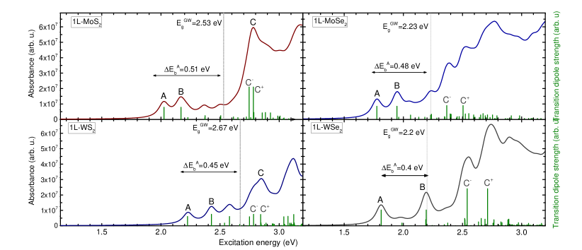
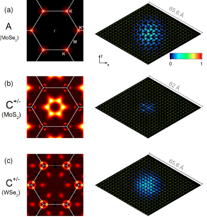
Figure 2 shows the imaginary parts of simulated dielectric functions of the widely researched monolayer molybdenum- and tungsten-based disulfides and diselenides exciton-paper , in good qualitative and quantitative agreement with recent theoretical reports by other groups and consistent with experimentally measured absorption spectra MoS2-absorption ; TMDC-absorption . For all four considered materials, the Coulomb attraction is sufficiently strong to pull a number of prominent absorption peaks well below the single-particle absorption onset given by the direct electronic band gaps. An analysis of the calculated excitonic wavefunctions, as shown for MoSe2 in Figure 3 (a), suggests that the lower-energy ’A’ peak originates from spin-conserving transitions over the direct band gaps at the K and K’ points in the hexagonal Brillouin zone. With this information, one can directly calculate the binding energy of the ’A’ electron-hole pairs as the difference between the exciton peak position (i.e. the optical band gap) and the corresponding electronic band gap. Here, a minor complication arises for tungsten-based materials, where the spin-order of the spin-orbit split conduction band minimum at the K and K’ points is reversed compared to molybdenum-based TMDCs; the lowest-energy direct transition between the valence band maximum is optically dark due to violation of spin-conservation while the transition to the second-lowest conduction band is optically bright andor-paper . With these considerations in mind, recent theoretical calculations yielded binding energies in the range of 0.4-0.5 eV for the four considered monolayer materials qiu-erratum ; wirtz-mos2-excitons ; gunnar-MoS2 ; komsa-excitons ; compmatdatabase ; Berkelbach-binding ; exciton-paper , well within the range of 0.3-0.5 eV reported from experiments chernikov-review ; Goryca2019 .
The large excitonic binding energies are mirrored in the significant spatial localization of the excitonic wavefunctions compared to typical length scales of Mott excitons in 3D semiconductor materials; we find Bohr radii on the order of about 2 nm for the ’A’ excitons in all four materials [refer to right side Figure 3 (a)]. The ’B’ peak arises from an excitonic transition between the energetically lower sub-band of the spin-orbit split valence band maximum at the K/K’ points to the spin-matched sub-band of the spin-orbit split conduction band minimum, thus appearing at slightly higher energies (mainly determined by the value of the spin-orbit splitting of the valence band), but with similar excitonic wavefunctions and exciton binding energies. The valence and conduction band extrema are completely spin-polarized at the K and K’ points, with the electron spin pointing in out-of-plane direction and the spin-order at the three K’ points of the hexagonal Brillouin zone reversed compared to the K points andor-paper , thus allowing for a valley-selective excitation of the A and B excitons using circularly polarized light TMDC-valley-pol .
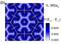
For monolayer MoS2 and WS2, the absorption spectra feature an additional prominent peak at an energy of about 2.75 eV, consistent with the broad ’C’ feature at this energy in experimentally measured absorption spectra MoS2-absorption ; WS2-absorption . Based on a decomposition of the calculated absorption spectra into the contributing transitions, the origin of this feature has been attributed to weakly spin-orbit split transitions between the valence and conduction bands at six points approximately half-way between the point and the ’Q’ conduction band valley exciton-paper ; qiu-2013 ; carvalho-band-nesting , refer to the momentum-resolved exciton wavefunction in Figure 3 (b). To avoid confusion, we note that it is common in the literature to label this valley by the index for the monolayer materials.
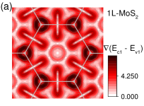
Using the value of the electronic band gap close to these six points, we derived a significant exciton binding energy on the order of 700 meV for MoS2, which is reflected in a small spatial extend of the exciton wavefunction [right side of Figure 3 (b)]. The location of the C excitations in the Brillouin zone appears somewhat unusual on first glance, as, in contrast to the A and B excitons, they do not correspond to transitions between valence and conduction band extrema. Instead, the C exciton arises from a ’band nesting’ of transitions between the approximately parallel valence and conduction bands halfway along the - line, see Figure 4 (a), thus leading to a high joint-density of states and a correspondingly high optical oscillator strength and optical conductivity carvalho-band-nesting .
As a consequence of this band nesting condition, it is to be expected that the location in the Brillouin zone, peak energy and optical oscillator strength of the C exciton or corresponding excitations should significantly depend on details of the electronic dispersion. As Figure 1 shows, the dispersion around the valence band maximum of MoSe2 and WSe2 is flatter and the conduction band dispersion is larger than in the disulfides, suggesting an increased repulsion between the transition metal and chalcogen states that make up the valence band (+) and the conduction band (+) edges at the point andor-paper . This weakens the band nesting condition on the - line [refer to Figure 4 (b) for the example of monolayer WSe2] and increases the difference between the transition energy at the band nesting points and the direct band gap of the system. At the same time, a set of six new band nesting points appear about half-way on the -K and -K’ lines. The absorption spectra of MoSe2 and WSe2 feature two particularly bright transitions, which give rise to two prominent broader features above an energy of 2.5 eV [Figure 2]. The calculated exciton wavefunctions [Figure 3 (c)] suggest that these excitations have significant contributions from transitions at the ’new’ band nesting point and hence can be interpreted as C excitons as well, albeit of a different origin than the C excitons in the disulfides. A significant qualitative consequence arises from the fact that the valence band edge at the band nesting point in monolayer MoSe2 and WSe2 retains some of the spin-orbit splitting from the and points, giving rise to two bright C excitations with a significant energetic splitting, in contrast to the very small splitting in the case of the disulfides. Similar results were found for monolayer MoTe2 as well exciton-paper .
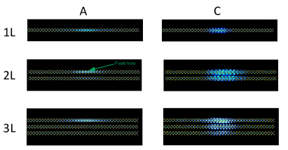
Another effect on the C excitons of TMDC materials could arise from interlayer or substrate interaction. The significant contributions from chalcogen states couple at the interface to adjacent materials, for instance a neighboring layer in bilayer Mo, and lead to hybridization-induced band splittings. Despite this interlayer hybridization, we reported previously exciton-paper that the resulting changes in the electronic dispersions are sufficiently small to retain the C excitons of the monolayer materials. In this context, the chalcogen contributions at the band nesting points have interesting consequences in terms of the spatial extent of the A and C exciton wavefunctions. At the K and K’ points, the valence band maximum and conduction band minimum are composed almost entirely of transition metal and orbitals, respectively, causing a negligible overlap and hybridization between the sub-bands of each material layer, particularly in light of the additional effect of spin-orbit coupling. As Figure 5 shows for the example of MoS2, this leads to a strong confinement of the electronic part of the exciton wavefunction to the layer where the hole is located. The A exciton in a molybdenum or tungsten TMDC homo-multilayer should hence behave like the A exciton of the corresponding monolayer material. For the C excitons, the chalcogen contributions to the conduction band result in a strong interlayer nature of the excitonic wavefunction, being significantly delocalized over the layers neighboring the layer where the hole is located. This interlayer nature might allow to resonantly couple a TMDC few-layer structure through optical excitation at the energy of C exciton, for instance activating interlayer resonant Raman modes in few-layer TMDCs (scheuschner-interlayer-modes, ; staiger-paper, ; wirtz-quantuminterference, ) that are not observed for excitation at the A exciton.
II.2 Electronic bandstructure of MoSe2/WSe2 heterostructures
In the following, we will first summarize our previous results gillen-interlayer on the electronic band structures and excitonic absorption spectra of lattice-commensurate MoSe2/WSe2 heterostructures with different stacking orders.
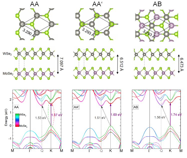
Figure 6 shows the electronic bands of vertically stacked MoSe2/WSe2 heterostructures obtained from GW calculations, which typically predict the electronic structures of materials with high accuracy, and were reported previously in Ref. [gillen-interlayer, ]. To estimate the influence of interlayer coupling on the electronic bandstructures of these heterostructures, we tested three different stacking orders that preserve the hexagonal symmetry. In the AA stacking order, the metal and selenium atoms of the two monolayers are located on top of each others. AA’ stacking corresponds to the AA stacking order with the upper layer rotated by 60∘ relative to the lower layer and is the energetically most stable stacking order in homobilayer and bulk TMDCs. In AB stacking order, on the other hand, the upper layer is shifted by 1/3(+) compared to AA stacking. Both AA and AB stacking orders are of -type due to their similarity to the stacking order in multilayer 3R-TMDCs, while AA’ stacking is of -type due to its similarity to the layer arrangement in 2H-TMDCs.
For all three stacking orders, the bands at the K point of the hexagonal Brillouin zone show only a weak hybridization, so that the bands can be directly assigned to the individual layers. This behavior is not unexpected, as the valence and conduction bands at the K and K’ points arise largely from transition-metal states and hence should only weakly ’feel’ the neighboring layer. Indeed, the bands form a type-II alignment, with the (global) valence band of the heterostructure contributed by the WSe2 layer, while the conduction band minima at the K and K’ points are located in the MoSe2 layer. The momentum-direct interlayer band gaps between these bands are somewhat stacking-dependent. As it is to be expected that AA and AB are the stacking-orders with the weakest and strongest interlayer coupling for all possible twist angles between the layers, the band gaps between the K and K’ of the individual materials should be generally fall within the range of of 1.65-1.75 eV. Our calculations further indicate that the intralayer band gaps at the K and K’ points of the individual materials are somewhat reduced by about 0.1 eV due to the dielectric screening provided by the respective other layer.
While the interlayer hybridization is very weak for the band around the K and K’ points, the situation is clearly different at other points in the Brillouin zone. The states at the local valence band maximum near the point and the conduction band minimum near the Q point, about half-way along the -K line, have significant contributions from Se states and couple strongly between the layers. Similarly to the homo-bilayer materials, this interlayer coupling transforms the heterostructure into an indirect semiconductor. The contribution of orbitals from the WSe2 layer to the conduction band minimum is stacking-order dependent and increases from 2̃0 % for AA stacking to about 40 % for AB stacking. Our results are in good agreement with other recent studies komsa-excitons ; wirtz-interlayer and establish that vertically stacked MoSe2/WSe2 heterobilayers, contrary to previous predictions, only feature a pseudo-type-II band alignment and an indirect fundamental band gap, which has possible implications for the nature and properties of the lowest-energy excitonic states of the material. Similar results have been found recently for MoS2/WS2 heterostructures as well wirtz-interlayer . In this case, the indirect fundamental band gap has been predicted to be between the Gamma and the K/K’ points, due to the smaller energy separation of the valence band maxima at the and K points in the individual monolayer molybdenum and tungsten disulfides.
The electronic bandstructures of the materials suggest two possible origins for the additional ’interlayer’ excitonic peaks seen in PL experiments: (i) Transitions at the interlayer band gaps at the K and K’ points of the Brillouin zone of the heterostructure. The optical strength of these transitions should then strongly depend on the twist angle between the materials, requiring an additional crystal momentum source for twist angles that break hexagonal symmetry. (ii) Transitions over the fundamental band gap, which is indirect for all twist angles.
II.3 Momentum-direct interlayer excitons in MoSe2/WSe2 heterostructures
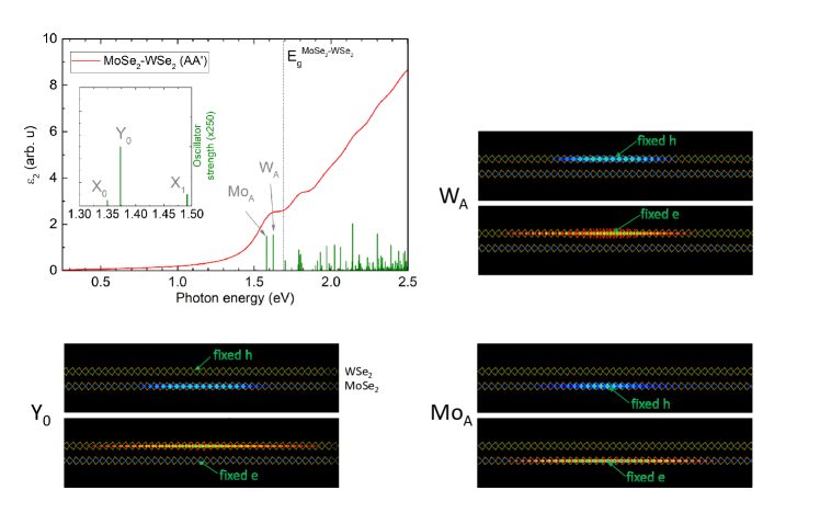
We recently reported the simulated absorption spectra of MoSe2/WSe2 heterostructures from solution of the excitonic Bethe-Salpeter equation, which includes effects from excitons with a vanishing center-of-mass momentum gillen-interlayer . Figure 7 shows the absorption spectrum for the AA’ stacked MoSe2/WSe2 heterostructure with the inclusion of spin-orbit coupling effects. The onset of absorbance is dominated by two transitions, and , which can readily be attributed to the excitons of individual monolayer MoSe2 and WSe2: our analysis of the k-resolved contributions to the exciton wavefunction shows that and exclusively arise from intralayer transitions between the MoSe2 (WSe2) bands at the K and K’ points. Further, the electron and hole parts of the excitonic wavefunctions show that the corresponding electron-hole pairs are completely confined to the MoSe2 and WSe2 layers, respectively [Figure 7]. In principle, one could directly derive the exciton binding energies from a comparison of the peak positions in the calculated absorption spectrum with the intralayer band gaps from Figure 6. However, while the 21x21 k-point grid used in the calculation is sufficient to give a very accurate qualitative picture of the excitonic spectrum, it does not yield fully converged peak positions and exciton binding energies. A second calculation using a denser 33x33 k-point grid (without inclusion of spin-orbit coupling) yields binding energies of about 310 meV and 290 meV for the and transitions, respectively, for the AA’ stacking order. This suggests that the additional dielectric screening induced by the neighboring layer reduced the binding energies of the intralayer excitons by about 150 meV.
| Exciton | Lifetimes | Stacking order | ||
| AA | AA’ | AB | ||
| ILX | (0) | 65.1 ps | 0.34 ns () | 737.6 ps () |
| 31.6 ps () | ||||
| 10.5 ns | 53.8 ns () | |||
| 5.34 ns () | ||||
| 213.2 ns () | ||||
| (0) | 0.34 ps | 0.37 ps | 0.41 ps | |
| 46.3 ps | 50.6 ps | 57.2 ps | ||
| (0) | 0.30 ps | 0.34 ps | 0.35 ps | |
| 25.1 ps | 29.5 ps | 29.0 ps |
In addition to these intralayer excitons, the computed absorption spectra also reveal two series of peaks of small optical oscillator strength at lower energies, see inset of Figure 7. These peaks arise from interlayer transitions between the WSe2-dominated global valence band maximum of the heterostructure to the spin-orbit-split conduction band minimum at the K and K’ points; the and peaks correspond to transitions to the lower energy and to the higher energy band, respectively. In the AA’ stacking order, the monolayer Brillouin zones of MoSe2 and WSe2 are rotated by 60∘ relative to each other, i.e. the K points of one material coincide with the K’ points of the other material. As a consequence, the transition should be brighter than the lower energy transition due to spin-conservation during the optical transition, while the transition should be dark in heterostructures with H-type stacking order. The excitonic wavefunction of the transition is shown in Figure 7. In contrast to the and transitions, the exciton wavefunction shows a clear spatial separation of the electron and hole pairs between the layers. From calculations with a denser k-point grid, we derive a rather large exciton binding energy of about 250 meV, which is of similar magnitude as that of the intralayer excitons. Our calculations thus suggest that the and peaks form two Rydberg series of interlayer excitons. Similar results were found for AA and AB stacking orders as well gillen-interlayer . Our calculations hence support the initial assignment of these PL peaks to interlayer excitons from momentum-direct excitations over the interlayer band gap at the K and K’ points of the heterostructure. The low oscillator strength of these transitions is in agreement with recent photocurrent measurements in MoSe2/WSe2 p-n junctions, which suggested that the oscillator strength of the intralayer excitons is 200 times larger than that of the interlayer excitons ross-MoSe2WSe2-pn . On the other hand, Torun et al. recently pointed out that the high exciton lifetime due to the spatial separation of the electron-hole pair, in complete agreement with experimental investigation of the interlayer peak wirtz-interlayer , is much larger than the exciton thermalization time. The high interlayer peak intensity in PL spectra can hence be understood from a Boltzmann-type thermal occupation of excitonic states, which compensates for the low oscillator strength of the interlayer excitons due to the energy separation to the intralayer excitonic states.
Due to depolarization effects in out-of-plane direction, only light with parallel polarization to the materials surface should appreciably couple to excitons in 2D materials palumno-2015 . This is indeed the case for the AA and AA’ stacking orders, where either the or the transitions are ’bright’ for parallel light polarization, but dark for ’perpendicular’ light polarization that is parallel to the surface normal vector (see supplementary material of Ref. [gillen-interlayer, ] for a comparison). On the other hand, neither nor show any appreciable oscillator strength for AB stacking gillen-interlayer . A detailed analysis revealed that this behavior can be traced back to variations in the optical selection rules for AB stacking compared to AA or AA’ stacking. The oscillator strength of the interlayer excitons largely arises from transitions between small contributions of MoSe2 states mixed into the valence band maximum at the K point into the MoSe2 dominated conduction band. For AB stacking these small contributions come from Mo states, which causes the interlayer transitions to be optically active for perpendicular polarized light, albeit with a much smaller optical oscillator strength than for AA or AA stacking. These results suggest that the stacking order can have a marked effect on the coupling of interlayer excitons to polarized light. As we show in the following, the small oscillator strength also has strong implicatons for the radiative lifetime of interlayer excitons for AB stacked MoSe2/WSe2 heterostructures.
Starting from Fermi’s Golden rule, an expression for the computation of radiative lifetimes of excitonic states in 2D materials from the excitonic oscillator strengths can be derived urbaszek-2014 ; palumno-2015 . Following this approach, the radiative recombination rate of the excitonic state with a small center-of-mass momentum emitting light polarized parallel to the 2D material plane is given by
with a zero-momentum lifetime
| (1) |
Thermal averaging of the radiative transition rate and inversion gives the averaged lifetime of exciton state for temperature palumno-2015 ,
| (2) |
These expressions assume a quadratic exciton dispersion, . The necessary ingredients, the zero-momentum exciton binding energies , the effective exciton mass and the transition dipole can be directly obtained from the GW bandstructures and solution of the BSE. is the total number of k-points in the grid used for the solution of the BSE. For AB stacking, Equation 2 is not applicable, as the recombination of interlayer excitons should not couple to parallel polarized light. We hence followed the approach used by Palumno et al. palumno-2015 to arrive at the following expressions of the momentum-dependent recombination rate and the thermally averaged lifetime for perpendicular polarized light:
| (3) |
Table 1 shows the calculated lifetimes for MoSe2/WSe2 heterostructures with three different stacking orders. The effective masses of the valence and conduction bands at are only weakly dependent on the stacking order and do not significantly affect the predicted lifetimes. For the intralayer excitons, the calculated optical oscillator strength decreases along the sequence AA’AAAB, which, according to Equations 2 and 3, causes a corresponding increase of the predicted radiative lifetimes. As expected from experimental data WSe2MoSe2-2 ; miller-MoSe2WSe2 ; lifetime-1 ; lifetime-2 ; Choi-2018 , the lifetimes of the interlayer excitons are predicted to be in the nanosecond range even for very low temperatures and thus significantly larger than those of the intralayer excitons. The stacking order has a marked effect on the predicted radiative lifetimes. For AA’ stacking, our calculated zero-momentum lifetime (0) is aproximately half the value reported recently from simulations using a combined Dirac-Bloch and gap equations approach meckbach and substantially larger (by a factor 3) than those reported for a bilayer MoSe2/WSe2 heterostructure by Palumno et al palumno-2015 . In the AA stacked heterostructure, the lifetime of the bright transition is more than twice as long as that of the transition for AA’ stacking. These differences might be related to different absolute magnitudes of the optical oscillator strengths. Due to the low oscillator strength even for perpendicular polarized light, we predict the the zero-momentum interlayer excitons for AB stacking to be extremely long-lived in terms of radiative decay time, on the order of microseconds; correspondingly, we expect non-radiative decay channels to be prevalent for interlayer excitons in AB stacked MoSe2/WSe2 heterostructures.
II.4 Momentum-indirect interlayer excitons in TMDC heterostructures
We will now turn towards the possible contribution of excitons with non-vanishing center-of-mass momentum, for example transitions related to the fundamental indirect band gap of TMDC heterostructures, to the ’interlayer’ peaks observed in PL experiments. Such an indirect transition has been proposed recently to be the origin of the prominent peak at 1.6 eV observed for lattice-incommensurate Mo/WSe2 heterostructures, in this case between the valence band maximum at the point of the heterostructure and the local minimum related to the K point of the Mo sublayer kunstmann-interlayer-excitons . An additional feature, which we attributed to the (momentum-indirect) transition, was observed at an energy of about 1 eV, in excellent agreement with theoretical simulations of the expected peak position Karni-Mos2Wse2 .
| Intralayer MoSe2 | Intralayer WSe2 | - | - | - | - | - | |
|---|---|---|---|---|---|---|---|
| Electronic | 1.98 | 1.97 | 1.71 | 1.69 | 1.51 | 1.69 | 1.87 |
| band gap | |||||||
| Exciton binding | 0.41 | 0.36 | 0.24 | 0.24 | 0.35 | 0.52 | 0.62 |
| energy (model) | |||||||
| Exciton binding | 0.3111footnotemark: 100footnotetext: 33x33x1 k-point grid without spin-orbit coupling | 0.2811footnotemark: 1 | 0.2511footnotemark: 1 | 0.2322footnotemark: 200footnotetext: 36x36x1 k-point grid without spin-orbit coupling | 0.2222footnotemark: 2 | 0.2922footnotemark: 2 | 0.2522footnotemark: 2 |
| energy (BSE) | |||||||
| Peak position model | 1.57 | 1.61 | 1.48 | 1.45 | 1.16 | 1.17 | 1.25 |
| BSE | 1.67 | 1.7 | 1.47 | 1.46 | 1.29 | 1.4 | 1.62 |
A simple and computationally efficient way to estimate the binding energies of excitons with non-zero center-of-mass momentum was proposed recently by Kunstmann et al., who used a four-band tight binding model together with input from DFT calculations to compare the predicted exciton peak positions in MoS2/WSe2 heterostructures with PL measurements kunstmann-interlayer-excitons . The resulting estimated binding energies of the ’momentum-direct’ exciton and the three ’momentum-indirect’ , , and excitons, as well as the predicted peak positions, are given in Table 2 for a MoSe2/WSe2 heterostructure with AA’ stacking order [refer to Sec. 2 of the SI for the input parameters to the tight-binding model extracted from our GW calculations]. The model appears to give an estimate of the exciton binding energy of the exciton that is in very good agreement with the BSE results, albeit at much lower computational cost. On the other hand, the model suggests that all three considered ’momentum-indirect’ excitons have binding energies similar to or larger than those of the intralayer excitons, which is expected to shift the and peaks below the experimentally observed peak positions. The predicted peak position of the transition is in somewhat better agreement. However, the different valence and conduction band extrema enter the model purely through their effective masses, band offsets and interlayer coupling parameters. Further, the dielectric screening entering the model is purely local and thus contains momentum-dependent screening effects only in an averaged way.
The Bethe-Salpeter Equation should be a more accurate and consistent approach, which also explicitly takes into account non-local interaction effects. However, the typical implementations of the BSE in solid state codes are aimed at the simulation of optical absorption spectra and hence only include contributions with vanishing center-of-mass momentum (). We hence extended the widely used YAMBO code yambo to solve the more general Bethe-Salpeter Equation bgw-2
| (4) |
for a finite exciton center-of-mass momentum . The band energies are typically quasiparticle energies obtained from G0W0 calculations. The exchange kernel
couples spin-conserving transitions, while the ’direct’ kernel
determines the formation of bound electron-hole pairs. Here, is the bare Coulomb interaction, is the screened Coulomb interaction, are form factors of the underlying interband transitions, and is a transferred momentum. The typical implementation of the BSE in most solid state physics codes is recovered by setting =.
In order to ensure meaningful quantitative results, we solved equation 4 using a grid of 36x36x1 k-points, neglecting effects from spin-orbit interaction. The obtained exciton binding energies are reported in Table 2. In stark contrast to the model calculations, the BSE predicts the binding energies of the excitons related to indirect electronic transitions in the MoSe2/WSe2 heterostructure to have very similar magnitudes as those of the exciton, in the range of 0.2-0.3 eV. We now find that a possible peak from the transition should be expected close to the intralayer excitonic peaks, suggesting that indeed should not contribute to the interlayer excitonic peak at lower energies. On the other hand, the peak energies of both the and excitons are predicted to be quite close to those of the exciton. As both excitons involve the -point conduction band minimum, inclusion of spin-orbit interaction should give rise to two peaks that are split by an energy of about 35 meV in both cases, in agreement with the recently reported experimental observation of momentum-indirect interlayer excitons hanbicki-MoSe2WSe2 .
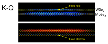
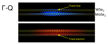
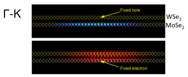
An advantage of the BSE is the access to the exciton wavefunctions for each predicted excitonic state in the system, in addition to the peak positions and exciton binding energies. Figure 8 shows the calculated electron and hole parts of the excitonic wavefunctions of the three considered ’indirect’ excitons. Based on the electronic bandstructures shown in Figure 6, one would expect that interlayer excitons have a much weaker layer confinement, and thus spatial separation, of the bound electrons and holes if or points are involved, due to the significant interlayer hybridization effects at these points in the Brillouin zone. Our calculations suggest that this assumption is indeed true for the hole part of the exciton wavefunction: For a hole located at the K point of the Brillouin zone, the corresponding wavefunction is confined to the WSe2 layer, while for a hole located at the point, the corresponding wavefunction has a strong interlayer nature with approximately equal weight on the two layers. This suggests that excitons involving -point holes should exhibit characteristically small exciton dipoles compared to the ’momentum-direct’ or excitons that exhibit a distinct interlayer charge separation. For excitons involving the point conduction band valley, the electron part of the exciton wavefunctions exhibits a small spilling of the electron into the WSe2 layer, while the larger part of the wavefunction is located in the MoSe2 layer. Based on an integration of the in-plane averaged electron part of the exciton wavefunction along the out-of-plane direction, we estimate this spill-over to be about 30 % of the electron wavefunction if spin-orbit interaction (SOI) is neglected. This coincides well with the relative contribution of electronic orbitals in the WSe2 layers to the Q conduction band valley (29 %, without SOI), which we estimated using the same method for the Kohn-Sham orbital of the conduction band minimum obtained from DFT. In general, the degree of charge separation for momentum-indirect interlayer excitons should depend significantly on the local stacking order: For an AA stacking order, which we expect to constitute the lowest limit in terms of interlayer hybridization, the contribution of the WSe2 layer to the DFT wavefunction of the Q valley conduction band minimum is reduced to 16 % (without SOI). We note that inclusion of SOI further increases the WSe2 layer weight to the DFT orbitals to 29 % for AA stacking and 40 % for AA’ stacking, respectively, in good agreement with the composition shown in Figure 6.
| AA | -5.95 () | -10.45 () | -16.88 () | -8.41 () | -12.16 () | 7.14 () | 4.68 () | |
|---|---|---|---|---|---|---|---|---|
| -5.89 | -10.38 | -16.80 | ||||||
| -5.00 | -9.27 | -13.88 | ||||||
| Exp | -8.511footnotemark: 100footnotetext: Ref. [Ciarrocchi-nature-MoSe2WSe2, ], -5.50.822footnotemark: 200footnotetext: Ref. [foerg2020moire, ] | |||||||
| AA’ | -16.48 () | -12.01 () | -5.65 () | -9.15 () | -12.98 () | -6.94 () | 0.4 () | |
| -16.4733footnotemark: 300footnotetext: 12x12x1 k-point grid | -12.0133footnotemark: 3 | -5.6533footnotemark: 3 | -9.1433footnotemark: 3 | -12.8233footnotemark: 333footnotemark: 3 | -5.3433footnotemark: 3 | -3.7633footnotemark: 3 | ||
| -16.34 | -11.87 | 5.55 | ||||||
| -13.6733footnotemark: 3 | -9.4133footnotemark: 3 | -4.8333footnotemark: 3 | -7.3933footnotemark: 3 | -11.0033footnotemark: 3 | -4.3533footnotemark: 3 | -3.4533footnotemark: 3 | ||
| -13.58 | -9.31 | 4.75 | ||||||
| Exp | 15.244footnotemark: 400footnotetext: Ref. [Wang2020, ], signs of g-factor not reported, -1655footnotemark: 500footnotetext: Ref. [Delhomme2020, ] | 10.744footnotemark: 4 | ||||||
| AB | -5.91 () | -10.43 () | -16.88 () | -8.11 () | -11.76 () | 6.10 () | 3.90 () | |
| -5.81 | -10.30 | -16.74 | ||||||
| -4.96 | -9.23 | -13.88 | ||||||
| Exp | 7.166footnotemark: 600footnotetext: Ref. [Ciarrocchi-nature-MoSe2WSe2, ] |
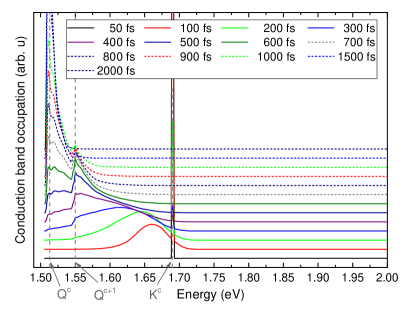
Clearly, an additional distinguishing factor between the ’direct’ and the ’indirect’ and excitons should be their temperature dependence, as the momentum-indirect excitons require the assistance of momentum sources for their formation and radiative recombination. In typical experiments, the excitation laser energy is too small for appreciable optical excitation at the and points and instead optically excites electrons at the and points. In order to obtain some insight into the scattering dynamics of optically excited electrons and the relevant timescales, we used the Boltzmann Transport Equation (BTE) as implemented in the PERTURBO code perturbo to calculate the time evolution of the conduction band occupations of an AA’ stacked MoSe2/WSe2 under the influence of electron-phonon coupling 111We used the Quantum ESPRESSO qe package to calculate the electronic structure and phonon spectra on a uniform grid of 9x9x1 k-points using the local density approximation and normconserving pseudopotentials from the PseudoDojo repository pseudodojo . The electronic wavefunctions were expanded in a planewave basis with a cutoff energy of 120 Ry, allowing for well converged phonon frequencies. We included spin-orbit coupling in our calculations and corrected the electronic structure with the GW corrections to match the electronic bands shown in Figure 6. Using the results of these results as input, we then used the PERTURBO code to calculate the temporal dynamics of excited electrons in the conduction bands. For this, we initially placed a charge of 0.1 in the conduction band minimum at each of the K and K’ points of the hexagonal Brillouin zone and propagated the band occupations through solution of the Boltzmann Transport Equation including electron-phonon coupling induced scattering for a simulation time of 2 ps and temperatures of 10 K and 300 K. To ensure an accurate representation of the scattering processes, a wannierization procedure was used to interpolate the electron-phonon matrix elements from a coarse 9x9x1 k-point grid to a dense 90x90x1 grid.. Selected snapshots of the energy-resolved conduction band occupation for a temperature of T=10 k are shown in Figure 9. Our calculations suggest that, neglecting the Coulomb interaction between electrons and holes, the electronic charge is efficiently scattered away from the / minima into the conduction band valley around the point by phonons with momenta slight smaller than within several 100 fs. We find a similar thermalization timescale if the initial charge is placed into the higher energy conduction bands at the K/K’ points that are contributed by the WSe2 layer [cf. Sec. 4 of the SI]. Due to the similar exciton binding energies, it would be a reasonable conclusion from these results that there should be a significant population of the global conduction band minimum at the point even at low temperatures, and thus of the lowest-energy excitons over the fundamental bad gap, competing with radiative recombination of 0 excitons at the / points of the heterostructure.
On the other hand, both recent magneto-optical experiments Ciarrocchi-nature-MoSe2WSe2 ; Wang2020 ; Delhomme2020 ; foerg2020moire and theoretical studies kunstmann-paper ; foerg2020moire suggest that the shift of interlayer exciton binding peak positions under external magnetic fields are a substantial factor for establishing the nature of the contributions to the interlayer excitonic peaks. It was found from magneto-luminescence measurements and similar techniques that the interlayer excitons of MoSe2/WSe2 heterostructures exhibit g-factors that (i) substantially differ from the g-factors of intralayer excitons in the monolayer TMDC materials (usually ) and (ii) show a strong dependence on the stacking order: While, for heterostructures in the R registry (e.g. the AA, AB stacking orders in the convention used in this paper), g-factors between 4.2 and 8.5 were found Ciarrocchi-nature-MoSe2WSe2 ; foerg2020moire , the interlayer exciton g-factors of heterostructures in the H registry are substantially higher, 15-16 for the energetically lowest contribution Wang2020 ; Delhomme2020 . Based on theoretical results from density functional theory calculations, the interlayer excitons have thus been interpreted to be zero-momentum singlet and triplet excitations at the and points.
The g-factor of a band transition between a valence band state with crystal momentum and a conduction band state at can be calculated from the relation deilmann-gfactor
with the band magnetic moments (in units of ) of valence and conduction bands,
Here, is the expectation value of spin momentum operator in out-of-plane direction , with spinor wavefunctions . is the corresponding orbital contribution to the magnetic moment and for a magnetic field in z-direction is given by the relation roth-gfactor
where is given by the momentum operator plus possible contributions from spin-orbit coupling kunstmann-paper . Both and can be extracted in a straightforward way from density functional theory calculations.
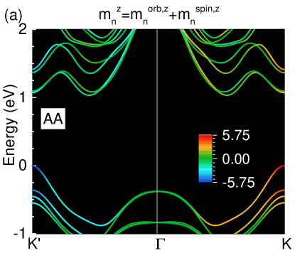
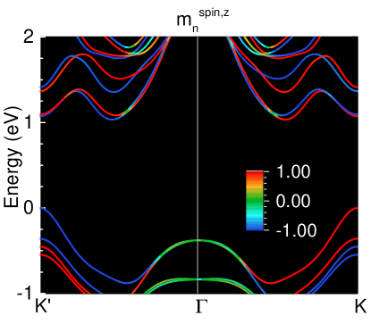
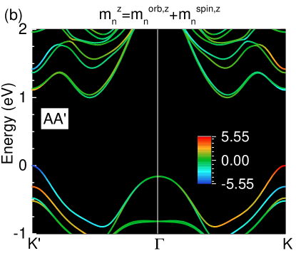
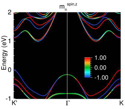
Within the typically implemented excitonic Bethe-Salpeter Equation formalism, the exciton is described by a weighted superposition of different interband transitions. With this, one can define an effective g-factor for an excitonic state with center-of-mass momentum by
where the excitonic wavefunction describes the weight of each transition contributing to the exciton. Depending on the exciton in question, the mixing of different transitions in the BSE approach might thus lead to somewhat different compared to for a given excitonic transition. For instance, Deilmann et al. reported recently deilmann-gfactor that even for the excitons of monolayer TMDCs, which are very localized in reciprocal space and consist to more than 95 % of a transition at the K/K’ points, the additional small contributions can lower compared to by about 30 %.

Table 3 shows the calculated effective exciton g-factors and band approximations for selected momentum-direct and -indirect excitons of an AA’ stacked MoSe2/WSe2 heterostructure222The values for the indirect excitons were obtained from calculations with a rather coarse 12x12x1 k-point grid, but explicit inclusion of spin-orbit coupling in the BSE calculations.. Plots of the underlying magnetic moments of valence and conduction bands and of the spin contribution for AA- and AA’-stackings are depicted in Figure 10. Our calculated values for are in reasonable agreement with previous theoretical studies and the experimental data and support the assignment of the interlayer excitons to a pair of momentum-direct singlet and triplet excitations at the and points. While the g-factors of the energetically lowest transitions show a certain dependence on the stacking order, this dependence appears to originate in changes in interband hybridization at the point. The induced variation of the g-factors and energetic order of the exciton with the higher and the exciton with the lower g-factor are not consistent with the available experimental data. A similar conclusion can be reached for the other momentum indirect excitons.
As expected from the previous reported results for the excitonic g-factors of the monolayer materials deilmann-gfactor , the inclusion of excitonic effects modifies the calculated effective g-factors of the MoSe2/WSe2 heterostructure. For the transitions and using the DFT band energies for the calculation of , the calculated are about 1 % smaller than the corresponding values, which validates the band approximation for description of the momentum-direct interlayer excitons. We note that when using a coarser 12x12 k-point grid for the solution of the BSE, the difference to is even smaller, due to the larger weight put on contributions at the and points in this case. The contributions to the indirect excitons are less localized in reciprocal space compared to the momentum-direct interlayer excitons and the differences between and are larger in this case. A further change appears if we use GW band energies for the calculation of : due to the larger energy differences, the calculated g-factors are substantially smaller than those calculated from DFT-level band energies. This somewhat decreases the agreement between the experimental data and the predicted g-factors for the excitons. The discrepancy might arise from the neglect of substrate and environmental effects in the simulations, affecting both the electronic band energies in the material and somewhat delocalizing the excitonic wavefunctions due to screening effects compared to the ’free-standing’ material in vacuum. Another possible source of discrepancy is the use of DFT spinors for the calculation of the orbital magnetic moments, which is not fully consistent with the use of G0W0 transition energies.
As an alternative to the interpretation of the doublet structure of the interlayer PL peak as a pair of charge-neutral excitons, Calman et al. geim-MoSe2WSe2 have recently suggested a pair of spatially indirect neutral exciton and spatially indirect negatively charged trion as the origin. A formalism for the estimation of the effective g-factor of trions was proposed and used by Lyons et al. for the interpretation of the trion valley Zeeman splitting in monolayer WSe2 lyons-trions . For a specific negatively charged trion configuration defined by the valley indices (+1 for the K point valleys, -1 for the K’ point valleys), the Zeeman splitting can be expressed through the relation
| (5) |
where is the trion effective g-factor due to valley- and spin-induced magnetic momenta, and are the exciton effective g-factor of the recombining electron-hole pair and the g-factor of an excess electron in a specific MoSe2-dominated conduction band valley, respectively. The effect of the recoil of the excess electron after recombination of the electron-hole pair on the Zeeman splitting is included through a Landau level associated g-factor . Here, is the effective mass of the excess electron, is the exciton effective mass, and is the trion effective mass. We derived the effective masses of the valence band maximum and the spin-orbit split conduction band valley from our calculated DFT bandstructures [cf. Section 2 of the SI]. This results in in the range of 1.8-2.2 for all considered trion configurations, very similar to the experimentally deducted value in monolayer WSe2 lyons-trions .
Based on Eq. 5, we calculated the trion effective g-factors for the three trion configurations shown in Figure 11 for the case of a AA’-stacked heterostructure. All three considered interlayer trion configurations consist of the bright neutral interlayer exciton and an excess electron in different conduction band valleys and have been predicted to occur in the optical absorption spectra of vertically stacked MoS2/WS2 deilmann-MoS2WS2 . The trion binding energies of 25-28 meV relative to the neutral interlayer exciton obtained in Ref. [deilmann-MoS2WS2, ] for the MoS2/WS2 heterostructure are similar to the trion binding energies predicted for TMDC monolayers Berkelbach-trions . Under the assumption of a similar binding energy in MoSe2/WSe2 heterostructures, all three trion configurations would give rise to absorption/emission peaks close to the ’darkish’ interlayer exciton. Our results suggest that the three configurations should exhibit characteristic g-factors in the range of 5-11, distinctively different from the g-factor of 16.5 predicted for the interlayer exciton.
Finally, we note that in principle, the exchange interaction between the three bound particles in the spin-triplet trion configuration shown in Figure 11 (b) should give rise to an exchange-induced Berry curvature lyons-trions ; Yu2014 , inducing an additional magnetic momentum and a g-factor contribution lyons-trions ( is the exchange splitting, is the free electron rest mass). For monolayer WSe2, this g-factor contribution has been estimated to be about 4, i.e. rather sizeable lyons-trions ; Yu2014 . However, due to the significant charge separation of electrons and holes in the case of the interlayer excitons and the associated trions, and thus the marginal spatial overlap between the electron and hole wavefunctions (about 1/1000th of the spatial overlap of the electron and hole wavefunctions of the and intralayer excitons), we estimate the g-factor contribution induced by electron-hole exchange to be negligibly small compared to the situation in the monolayer materials.
II.5 C-type excitons in AA’-stacked MoSe2/WSe2 heterostructures
In this section, we will go beyond the excitons around the absorption onset and consider the composition of the optical absorption at slightly larger energies. As we showed in section II.2, the absorption spectra of monolayer molybdenum and tungsten based TMDCs feature strongly bound ’C’ excitons, which arise from a high joint-density-of-states between valence and conduction bands. The fulfillment of these band nesting conditions depend on details in the electronic structure. At the same time, the electronic contribution to the wavefunction of the monolayer C excitons feature a noticeable component that points in out-of-plane direction, which we found gave rise to a significant spatial interlayer delocalization of the excitonic wavefunctions for TMDC homobi- and trilayers. An interesting question is then how the tightly bound C excitons are affected by formation of a heterostructure.
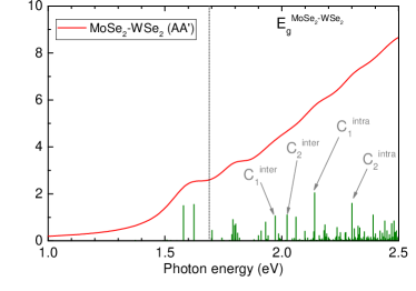
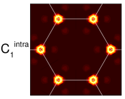
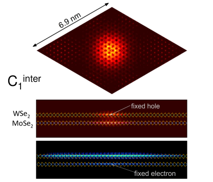
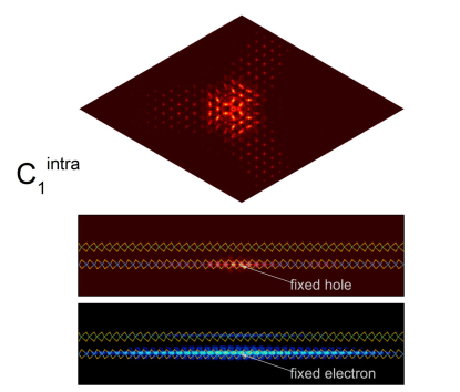
The calculated optical spectrum of a AA’ stacked MoSe2/WSe2 heterostructure shows a number of peaks with higher oscillator strength in the energy range of 2.0-2.5 eV, where the C excitons of monolayer MoSe2 and WSe2 are located. In the following, we will focus on four of these bright transitions, as labeled in Figure 12. These states have in common that their k-resolved excitonic wavefunctions, i.e. the location of the band transitions contributing to the excitonic state in the Brillouin zone of the material, are very similar to those of the C excitons in monolayer MoSe2 and WSe2. Figure 13 shows the calculated k-resolved exciton wavefunctions. In all four cases, the strongest contributions come from the direct vicinities of the K and K’ points, with additional contributions from a ’special’ point on the lines. As for the monolayer materials, the location of this special point is given by a band nesting between valence and conduction bands, which appears to be present in the slightly modified electrionic bandstructure of the heterostructure as well. This suggests that all four selected absorption peaks are ’C-like’.
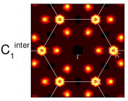
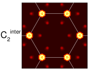
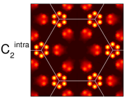
As the plots of the real-space excitonic wavefunctions in Figure 14 show, we can divide the four selected transitions into two groups: Two transitions at lower energies, and , show a distinct interlayer nature. arises from transitions from the WSe2-dominated valence band into the MoSe2-dominated lowest conduction band, which, interestingly, suggests that the slope of these two bands is sufficiently similar to establish an effective band nesting condition even between bands contributed by different materials. The corresponding excitonic wavefunction shows a clear confinement of the hole part to the WSe2 layer, while the electron part is mostly located in the MoSe2 layer, but spills over into neighboring WSe2 layer, similar to the exciton wavefunction in MoSe2 homobilayers. The electronic part of the exciton wavefunction shows a bright and localized ’core’ with some additional density tail from band-like states of similar energy that are mixed into the exciton wavefunction. This localization is also mirrored in the exciton binding energy: based on the energy difference between the highest valence and the lowest conduction band at the special point, which our calculations indicate to have the largest contribution to the exciton, we estimate the exciton binding energy to be about 453 meV.
The situation is somewhat reversed for : here, the largest contributions come from transitions at the K and K’ points and their immediate vicinity, between the second and third highest valence bands (of purely MoSe2 or WSe2 nature) into the third lowest conduction band, which is contributed by the WSe2 layer, see the electronic bandstructure shown in Figure 6. Smaller contributions come from transitions at the band nesting point, between the valence band top and the hybridized second lowest conduction band. Consequently, it is the hole part of the excitonic wavefunction that shows a distinct interlayer delocalization in this case, with the larger share of the hole being located in the MoSe2 layer, while the electronic part is well-localized in the WSe2 and only shows a minor spilling into the neighboring material. Within the layer, the electron appears to be well localized, with an exciton radius of about 35 Å. Based on the energy difference between the initial and final states at the point and the exciton peak position, we estimate the exciton binding energy to be 448 meV. We can thus understand and as ’interlayer C excitons’, with a noticeable interlayer separation of bound electrons and holes.

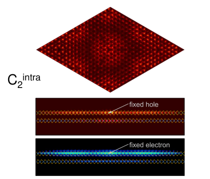
In contrast to the previous two states, the second group of transitions can be more or less clearly be attributed to arise from individual layer and thus have a noticeable intralayer nature. consists of a mix of almost degenerate MoSeWSe2 transitions close to the and points and additional C-like transitions away from . Despite this, we find that the exciton wavefunction has a significant intralayer nature centered on the MoSe2 layer and the electron part is quite localized. In terms of both spatial distribution and contributions in reciprocal space, appears to be analogous to the C excitons in mono- and bilayer MoSe2. From a weighted average of the energies of the transitions contributing to the exciton wavefunctions, the binding energy is calculated to be 400 meV. The transition, on the other hand, mainly consists of intralayer transitions within the WSe2 layer and thus has some resemblance to the C excitons of WSe2. Quite surprisingly, while the electron and hole parts of the exciton wavefunction appear to be quite delocalized, we calculate a rather high exciton binding energy of 414 meV from the difference of the peak energy to a weighted average of the energies of the constituing band transitions. It is thus possible that the calculated peak in fact consists of an exciton mixed with band transitions of similar energy, which gives rise to an extended wavefunction. A more detailed decomposition would be necessary to draw further conclusions on the nature of the peak.
III Summary
We have expanded on our previous study on the excitonic spectra of vertically stacked MoSe2/WSe2 heterostructures. The previously reported significantly stacking-dependent optical oscillator strengths of the lowest energy interlayer excitons lead to a wide range of radiative lifetimes. In particular, deriving an equation for excitons emitting out-of-plane polarized light, we were able to quantify the radiative lifetime of the ’brightish’ interlayer excitons in AB-stacked heterostructures to 200 ns (at T=4 K), significantly larger than the lifetimes obtained for the investigated AA and AA’ stacking orders. We expect these results to be transferable to other stacking orders as well.
By virtue of implementation and solution of the finite-momentum Bethe-Salpeter Equation, we further studied the binding energies and wavefunctions of relevant momentum indirect excitons between the valence and conduction band valleys. Here, we showed from ab initio that the momentum-indirect excitons over the fundamental band gap () should be the lowest-energy excitons for ideally stacked MoSe2/WSe2 heterostructures, about 0.15 eV below the momentum-direct excitations with a significant decrease of spatial charge separation due to interlayer hybridization effects. Experimental observation of such momentum-indirect interlayer excitons have been reported recently by Hanbicki et al hanbicki-MoSe2WSe2 . Simulations of the carrier dynamics of free electrons suggest that the global conduction band minimum should be quickly populated after optical excitation in resonance with the intralayer ’A’ excitons. Despite these results, our calculations of the effective exciton Landé g-factors confirm previous reports that the experimentally observed interlayer exciton magnetoluminescence in bilayer MoSe2/WSe2 heterostructures probably stems from (quasi-)momentum direct interlayer excitons. Particularly compared to the TMDC homobilayers and the related MoS2/WS2 heterostructures this raises the question why the excitons do not appear to be commonly observed in photoluminescence measurements of MoSe2/WSe2 bilayer heterostructures. Future theoretical and experimental work might shed further light on, e.g. the influence of the moiré potential on the interlayer excitonic and trionic spectra.
Analyzing the calculated absorption spectra, we further reveal the existence of higher energy interlayer excitons with a larger delocalization in reciprocal space and high binding energy, which can be interpreted as interlayer analog to the prominent C excitons in TMDCs mono- and few-layer materials.
IV Acknowledgements
Computational resources used for the simulations in this work were provided by the North-German Supercomputing Alliance (HLRN) under Project bep00047 and by the Regional Computing Center Erlangen (RRZE).
References
- (1) K. S. Novoselov, A. K. Geim, S. V. Morozov, D. Jiang, Y. Zhang, S. V. Dubonos, I. V. Grigorieva, A. A. Firsov, Science 2004, 36 666.
- (2) K. S. Novoselov, D. Jiang, F. Schedin, T. J. Booth, V. V. Khotkevich, S. V. Morozov, A. K. Geim, PNAS 2005, 102 10451.
- (3) N. Mounet, M. Gibertini, P. Schwaller, D. Campi, A. Merkys, A. Marrazzo, T. Sohier, I. E. Castelli, A. Cepellotti, G. Pizzi, N. Marzari, Nature Nanotechnology 2018, 13, 3 246.
- (4) G. Cheon, E. D. Cubuk, E. R. Antoniuk, L. Blumberg, J. E. Goldberger, E. J. Reed, The Journal of Physical Chemistry Letters 2018, 9, 24 6967.
- (5) K. F. Mak, C. Lee, J. Hone, J. Shan, T. F. Heinz, Phys. Rev. Lett. 2010, 105 136805.
- (6) A. Splendiani, L. Sun, Y. Zhang, T. Li, J. Kim, C.-Y. Chim, G. Galli, F. Wang, Nano Lett. 2010, 10 1271.
- (7) S. Tongay, J. Suh, C. Ataca, W. Fan, A. Luce, J. S. Kang, J. Liu, C. Ko, R. Raghunathanan, J. Zhou, F. Ogletree, J. Li, J. C. Grossman, J. Wu, Sci. Rep. 2013, 3 2657.
- (8) H. R. Gutierrez, N. Perea-Lopez, A. L. Elías, A. Berkdemir, B. Wang, R. Lv, F. Lopez-Urias, V. H. Crespi, H. Terrones, M. Terrones, Nano Lett. 2012, 13 3447.
- (9) S. Mouri, Y. Miyauchi, K. Matsuda, Nano Lett. 2013, 13 5944.
- (10) N. Scheuschner, O. Ochedowski, A.-M. Kaulitz, R. Gillen, M. Schleberger, J. Maultzsch, Phys. Rev. B 2014, 89 125406.
- (11) The G0W0 simulations in Figure 1 were performed with the BerkeleyGW code, using 2000 unoccupied bands in combination with the static remainder method to account for higher-energy interband transitions. The band energies were extrapolated to infinite cutoff energy for the correlation contribution with the method we employed previously in Ref. gillen-interlayer, and calculations for cutoff energies of 250 eV, 300 eV and 350 eV, for which the variation of band energies is linear with the inverse of the number of included reciprocal lattice vectors. A homogeneous 9x9 k-point grid together with the ”Nonuniform Neck Subsampling” method nns was sufficient to converge the electronic band gap to less than 0.05 eV. The effect of spin-orbit interaction was included a posteriori by extracting the spin-orbit-induced band splittings on the DFT level of theory and adding the extracted values to the GW band energies. The electronic band structures were calculated through Wannier interpolation using the Wannier90 wannier90 code. The input electronic energies and wavefunctions and the groundstate density for the GW and Wannier calculations were computed with the Quantum Espresso code, optimized norm-conserving Vanderbilt pseudopotentials oncv , a cutoff energy of 90 Ry and a 12x12x1 k-point grid (for the groundstate calculations). The atomic positions and lattice vectors were relaxed using the method outlined in Ref. [36].
- (12) A. R. Klots, A. K. M. Newaz, B. Wang, D. Prasai, H. Krzyzanowska, J. Lin, D. Caudel, N. J. Ghimire, J. Yan, B. L. Ivanov, K. A. Velizhanin, A. Burger, D. G. Mandrusan, N. H. Tolk, S. T. Pantelides, K. I. Bolotin, Scientific Reports 2014, 4 6608.
- (13) K. He, N. Kumar, L. Zhao, Z. Wang, K. F. Mak, H. Zhao, J. Shan, Phys. Rev. Lett. 2014, 113 026803.
- (14) M. M. Ugeda, A. J. Bradley, S.-F. Shi, F. H. da Jornada, Y. Zhang, D. Y. Qiu, W. Ruan, S.-K. Mo, Z. Hussain, Z.-X. Shen, F. Wang, S. G. Louie, M. F. Crommie, Nature Materials 2014, 13 1091.
- (15) B. Zhu, X. Chen, X. Cui, Scientific Reports 2015, 5, 1 9218.
- (16) H. M. Hill, A. F. Rigosi, C. Roquelet, A. Chernikov, T. C. Berkelbach, D. R. Reichman, M. S. Hybertsen, L. E. Brus, T. F. Heinz, Nano Letters 2015, 15, 5 2992.
- (17) C. Zhang, Y. Chen, A. Johnson, M.-Y. Li, L.-J. Li, P. C. Mende, R. M. Feenstra, C.-K. Shih, Nano Letters 2015, 15, 10 6494.
- (18) A. F. Rigosi, H. M. Hill, K. T. Rim, G. W. Flynn, T. F. Heinz, Phys. Rev. B 2016, 94 075440.
- (19) G. Wang, A. Chernikov, M. M. Glazov, T. F. Heinz, X. Marie, T. Amand, B. Urbaszek, Rev. Mod. Phys. 2018, 90 021001.
- (20) M. Goryca, J. Li, A. V. Stier, T. Taniguchi, K. Watanabe, E. Courtade, S. Shree, C. Robert, B. Urbaszek, X. Marie, S. A. Crooker, Nature Communications 2019, 10, 1 4172.
- (21) D. Y. Qiu, F. H. da Jornada, S. G. Louie, Phys. Rev. Lett. 2013, 111 216805.
- (22) R. Gillen, J. Maultzsch, IEEE Journal of Selected Topics in Quantum Electronics 2017, 23, 1 219.
- (23) A. Carvalho, R. M. Ribeiro, A. H. Castro Neto, Phys. Rev. B 2013, 88 115205.
- (24) S. Lin, X. Li, P. Wang, Z. Xu, S. Zhang, H. Zhong, Z. Wu, W. Xu, H. Chen, Scientific Reports 2015, 5 15103.
- (25) F. Withers, O. D. Pozo-Zamudio, A. Mishchenko, A. P. Rooney, A. Gholinia, K. Watanabe, T. Taniguchi, S. J. Haigh, A. K. Geim, A. I. Tartakovskii, K. S. Novoselov, Nature Materials 2015, 14 301.
- (26) O. Lopez-Sanchez, D. Lembke, M. Kayci, A. Radenovic, A. Kis, Nature Nanotechnology 2013, 8 497.
- (27) P. Tonndorf, R. Schmidt, R. Schneider, J. Kern, M. Buscema, G. A. Steele, A. Castellanos-Gomez, H. S. J. van der Zant, S. M. de Vasconcellos, R. Bratschitsch, Optica 2015, 4 347.
- (28) Y.-M. He, G. Clark, J. R. Schaibley, Y. He, M.-C. Chen, Y.-J. Wei, X. Ding, Q. Zhang, W. Yao, X. Xu, C.-Y. Lu, J.-W. Pan, Nature Nanotechnology 2015, 10 497.
- (29) C. Chakraborty, L. Kinnischtzke, K. M. Goodfellow, R. Beams, A. N. Vamivakas, Nature Nanotechnology 2015, 10 507.
- (30) A. Srivastava, M. Sidler, A. V. Allain, D. S. Lembke, A. Kis, A. Imamoǧlu, Nature Nanotechnology 2015, 10 491.
- (31) D. Xiao, G.-B. Liu, W. Feng, X. Xu, W. Yao, Phys. Rev. Lett. 2012, 108 196802.
- (32) O. L. Sanchez, D. Ovchinnikov, S. Misra, A. Allain, A. Kis, Nano Letters 2016, 16, 9 5792.
- (33) Y. Yu, S. Hu, L. Su, L. Huang, Y. Liu, Z. Jin, A. A. Purezky, D. B. Geohegan, K. W. Kim, Y. Zhang, L. Cao, Nano Letters 2015, 15, 1 486.
- (34) H. Fang, C. Battaglia, C. Carraro, S. Nemsak, B. Ozdol, J. S. Kang, H. A. Bechtel, S. B. Desai, F. Kronast, A. A. Unal, G. Conti, C. Conlon, G. K. Palsson, M. C. Martin, A. M. Minor, C. S. Fadley, E. Yablonovitch, R. Maboudian, A. Javey, PNAS 2014, 111 6198.
- (35) J. Kunstmann, P. N. F. Mooshammer, A. Chaves, N. P. F. Stein, G. Plechinger, C. Strunk, C. Schüller, G. Seifert, D. Reichman, T. Korn, Nature Physics 2018, 14 801.
- (36) O. Karni, E. Barré, S. C. Lau, R. Gillen, E. Y. Ma, B. Kim, K. Watanabe, T. Taniguchi, J. Maultzsch, K. Barmak, R. H. Page, T. F. Heinz, Phys. Rev. Lett. 2019, 123 247402.
- (37) P. Rivera, J. R. Schaibley, A. M. Jones, J. S. Ross, S. Wu, G. Aivazian, P. Klement, K. Seyler, G. Clark, N. J. Ghimire, J. Yan, D. G. Mandrus, W. Yao, X. Xu, Nature Communications 2015, 6 6242.
- (38) J. S. Ross, P. Rivera, J. Schaibley, E. Lee-Wong, H. Yu, T. Taniguchi, K. Watanabe, J. Yan, D. Mandrus, D. Cobden, W. Yao, X. Xu, Nano Letters 2017, 17, 2 638.
- (39) P. K. Nayak, Y. Horbatenko, S. Ahn, G. Kim, J.-U. Lee, K. Y. Ma, A.-R. Jang, H. Lim, D. Kim, S. Ryu, H. Cheong, N. Park, H. S. Shin, ACS Nano 2017, 11, 4 4041.
- (40) K. Tran, G. Moody, F. Wu, X. Lu, J. Choi, K. Kim, A. Rai, D. A. Sanchez, J. Quan, A. Singh, J. Embley, A. Zepeda, M. Campbell, T. Autry, T. Taniguchi, K. Watanabe, N. Lu, S. K. Banerjee, K. L. Silverman, S. Kim, E. Tutuc, L. Yang, A. H. MacDonald, X. Li, Nature 2019, 567, 7746 71.
- (41) E. V. Calman, L. H. Fowler-Gerace, D. J. Choksy, L. V. Butov, D. E. Nikonov, I. A. Young, S. Hu, A. Mishchenko, A. K. Geim, Nano Letters 2020, 20, 3 1869.
- (42) D. Kozawa, A. Carvalho, I. Verzhbitskiy, F. Giustiniano, Y. Miyauchi, S. Mouri, A. H. C. Neto, K. Matsuda, G. Eda, Nano Lett. 2016, 16 4087.
- (43) F. Ceballos, M. Z. Bellus, H.-Y. Chiu, H. Zhao, Nanoscale 2015, 7 17523.
- (44) B. Miller, A. Steinhoff, B. Pano, J. Klein, F. Jahnke, A. Holleitner, U. Wurstbauer, Nano Letters 2017, 17, 9 5229.
- (45) J. Kang, S. Tongay, J. Zhou, J. Li, J. Wu, Appl. Phys. Lett. 2013, 102 012111.
- (46) M. M. Furchi, A. A. Zechmeister, F. Hoeller, S. Wachter, A. Pospischil, T. Mueller, IEEE Journal of Selected Topics in Quantum Electronics 2017, 23, 1 106.
- (47) A. T. Hanbicki, H.-J. Chuang, M. R. Rosenberger, C. S. Hellberg, S. V. Sivaram, K. M. McCreary, I. I. Mazin, B. T. Jonker, ACS Nano 2018, 12, 5 4719.
- (48) A. Ciarrocchi, D. Unuchek, A. Avsar, K. Watanabe, T. Taniguchi, A. Kis, Nature Photonics 2019, 13, 2 131.
- (49) T. Wang, S. Miao, Z. Li, Y. Meng, Z. Lu, Z. Lian, M. Blei, T. Taniguchi, K. Watanabe, S. Tongay, D. Smirnov, S.-F. Shi, Nano Letters 2020, 20, 1 694.
- (50) A. Delhomme, D. Vaclavkova, A. Slobodeniuk, M. Orlita, M. Potemski, D. M. Basko, K. Watanabe, T. Taniguchi, D. Mauro, C. Barreteau, E. Giannini, A. F. Morpurgo, N. Ubrig, C. Faugeras, 2D Materials 2020, 7, 4 041002.
- (51) M. Förg, A. S. Baimuratov, S. Y. Kruchinin, I. A. Vovk, J. Scherzer, J. Förste, V. Funk, K. Watanabe, T. Taniguchi, A. Högele, Moiré excitons in mose2-wse2 heterobilayers and heterotrilayers, 2020.
- (52) M. Okada, A. Kutana, Y. Kureishi, Y. Kobayashi, Y. Saito, T. Saito, K. Watanabe, T. Taniguchi, S. Gupta, Y. Miyata, B. I. Yakobson, H. Shinohara, R. Kitaura, ACS Nano 2018, 12, 3 2498.
- (53) K. L. Seyler, P. Rivera, H. Yu, N. P. Wilson, E. L. Ray, D. G. Mandrus, J. Yan, W. Yao, X. Xu, Nature 2019, 567 66.
- (54) R. Gillen, J. Maultzsch, Phys. Rev. B 2018, 97 165306.
- (55) M. Förg, A. S. Baimuratov, S. Y. Kruchinin, I. A. Vovk, J. Scherzer, J. Förste, V. Funk, K. Watanabe, T. Taniguchi, A. Högele, arXiv e-prints 2020, arXiv:2006.09105.
- (56) M. Palummo, M. Bernardi, J. C. Grossman, Nano Letters 2015, 15, 5 2794.
- (57) S. Latini, K. T. Winther, T. Olsen, K. S. Thygesen, Nano Letters 2017, 17, 2 938.
- (58) E. Torun, H. P. C. Miranda, A. Molina-Sánchez, L. Wirtz, Phys. Rev. B 2018, 97 245427.
- (59) T. Deilmann, K. S. Thygesen, Nano Letters 2018, 18, 2 1460.
- (60) X. Lu, X. Li, L. Yang, Phys. Rev. B 2019, 100 155416.
- (61) N. Scheuschner, R. Gillen, M. Staiger, J. Maultzsch, Phys. Rev. B 2015, 91 235409.
- (62) H. P. C. Miranda, S. Reichardt, G. Froehlicher, A. Molina-Sánchez, S. Berciaud, L. Wirtz, Nano Letters 2017, 17, 4 2381.
- (63) A. Molina-Sánchez, M. Palummo, A. Marini, L. Wirtz, arXiv:1604.00943 2016.
- (64) A. Chernikov, T. C. Berkelbach, H. Hill, A. Rigosi, Y. Li, O. B. Aslan, D. R. Reichman, M. S. H. abnd T. F. Heinz, Phys. Rev. Lett. 2014, 113 076802.
- (65) K. P. Dhakal, D. L. Duong, J. Lee, H. Nam, M. Kim, M. Kan, Y. H. Lee, J. Kim, Nanoscale 2014, 6 13028.
- (66) H. Li, M. Qin, L. Wang, X. Zhai, R. Ren, J. Hu, Opt. Express 2017, 25, 25 31612.
- (67) A. Kormányos, G. Burkard, M. Gmitra, J. Fabian, V. Zólyomi, N. D. Drummond, V. Fal’ko, 2D Mater. 2015, 2 022001.
- (68) D. Y. Qiu, F. H. da Jornada, S. G. Louie, Phys. Rev. Lett. 2015, 115 119901.
- (69) A. Molina-Sánchez, D. Sangalli, K. Hummer, A. Marini, L. Wirtz, Phys. Rev. B 2013, 88 045412.
- (70) G. Berghäuser, E. Malic, Phys. Rev. B 2014, 89 125309.
- (71) H.-P. Komsa, A. V. Krasheninnikov, Phys. Rev. B 2012, 86 241201.
- (72) F. A. Rasmussen, K. S. Thygesen, The Journal of Physical Chemistry C 2015, 119, 23 13169.
- (73) R. Tempelaar, T. C. Berkelbach, Nature Communications 2019, 10, 1 3419.
- (74) D. Xiao, G.-B. Liu, W. Feng, X. Xu, W. Yao, Phys. Rev. Lett. 2012, 108 196802.
- (75) B. Zhu, X. Chen, X. Cui, Scientific Reports 2015, 5, 1 9218.
- (76) M. Staiger, R. Gillen, N. Scheuschner, O. Ochedowski, F. Kampmann, M. Schleberger, C. Thomsen, J. Maultzsch, Phys. Rev. B 2015, 91 195419.
- (77) H. P. C. Miranda, S. Reichardt, G. Froehlicher, A. Molina-Sánchez, S. Berciaud, L. Wirtz, Nano Letters 2017, 17, 4 2381.
- (78) J. S. Ross, P. Rivera, J. Schaibley, E. Lee-Wong, H. Yu, T. Taniguchi, K. Watanabe, J. Yan, D. Mandrus, D. Cobden, W. Yao, X. Xu, Nano Letters 2017, 17, 2 638.
- (79) M. M. Glazov, T. Amand, X. Marie, D. Lagarde, L. Bouet, B. Urbaszek, Phys. Rev. B 2014, 89 201302.
- (80) P. Rivera, K. L. Seyler, H. Yu, J. R. Schaibley, J. Yan, D. G. Mandrus, W. Yao, X. Xu, Science 2016, 351, 6274 688.
- (81) P. Nagler, G. Plechinger, M. V. Ballottin, A. Mitioglu, S. Meier, N. Paradiso, C. Strunk, A. Chernikov, P. Christianen, C. Schüller, T. Korn, 2D Mater. 2017, 4 025112.
- (82) C. Choi, J. Huang, H.-C. Cheng, H. Kim, A. K. Vinod, S.-H. Bae, V. O. Özçelik, R. Grassi, J. Chae, S.-W. Huang, X. Duan, K. Kaasbjerg, T. Low, C. W. Wong, npj 2D Materials and Applications 2018, 2, 1 30.
- (83) L. Meckbach, U. Huttner, L. C. Bannow, T. Stroucken, S. W. Koch, J. Phys: Condens. Matter 2018, 30 374002.
- (84) A. Marini, C. Hogan, M. Grüning, D. Varsano, Comp. Phys. Comm. 2009, 180 1392.
- (85) M. Rohlfing, S. G. Louie, Phys. Rev. B 2000, 62 4927.
- (86) J.-J. Zhou, J. Park, I.-T. Lu, I. Maliyov, X. Tong, M. Bernardi, arXiv e-prints 2020.
- (87) We used the Quantum ESPRESSO qe package to calculate the electronic structure and phonon spectra on a uniform grid of 9x9x1 k-points using the local density approximation and normconserving pseudopotentials from the PseudoDojo repository pseudodojo . The electronic wavefunctions were expanded in a planewave basis with a cutoff energy of 120\tmspace+.1667emRy, allowing for well converged phonon frequencies. We included spin-orbit coupling in our calculations and corrected the electronic structure with the GW corrections to match the electronic bands shown in Figure 6. Using the results of these results as input, we then used the PERTURBO code to calculate the temporal dynamics of excited electrons in the conduction bands. For this, we initially placed a charge of 0.1\tmspace+.1667em in the conduction band minimum at each of the K and K’ points of the hexagonal Brillouin zone and propagated the band occupations through solution of the Boltzmann Transport Equation including electron-phonon coupling induced scattering for a simulation time of 2\tmspace+.1667emps and temperatures of 10\tmspace+.1667emK and 300\tmspace+.1667emK. To ensure an accurate representation of the scattering processes, a wannierization procedure was used to interpolate the electron-phonon matrix elements from a coarse 9x9x1 k-point grid to a dense 90x90x1 grid.
- (88) T. Woźniak, P. E. Faria Junior, G. Seifert, A. Chaves, J. Kunstmann, Phys. Rev. B 2020, 101 235408.
- (89) T. Deilmann, P. Krüger, M. Rohlfing, Phys. Rev. Lett. 2020, 124 226402.
- (90) L. M. Roth, Phys. Rev. 1960, 118 1534.
- (91) The values for the indirect excitons were obtained from calculations with a rather coarse 12x12x1 k-point grid, but explicit inclusion of spin-orbit coupling in the BSE calculations.
- (92) T. Lyons, S. Dufferwiel, M. Brooks, F. Withers, T. Taniguchi, K. Watanabe, K. S. Novoselov, G. Burkard, A. I. Tartakovskii, Nature Comm. 2019, 10 2330.
- (93) T. C. Berkelbach, M. S. Hybertsen, D. R. Reichman, Phys. Rev. B 2013, 88 045318.
- (94) H. Yu, G.-B. Liu, P. Gong, X. Xu, W. Yao, Nature Communications 2014, 5, 1 3876.
- (95) F. H. da Jornada, D. Y. Qiu, S. G. Louie, Phys. Rev. B 2017, 95 035109.
- (96) A. A. Mostofi, J. R. Yates, G. Pizzi, Y.-S. Lee, I. Souza, D. Vanderbilt, N. Marzari, Computer Physics Communications 2014, 185, 8 2309 .
- (97) D. R. Hamann, Phys. Rev. B 2013, 88 085117.
- (98) P. Giannozzi, S. Baroni, N. Bonini, M. Calandra, R. Car, C. Cavazzoni, D. Ceresoli, G. L. Chiarotti, M. Cococcioni, I. Dabo, A. D. Corso, S. de Gironcoli, S. Fabris, G. Fratesi, R. Gebauer, U. Gerstmann, C. Gougoussis, A. Kokalj, M. Lazzeri, L. Martin-Samos, N. Marzari, F. Mauri, R. Mazzarello, S. Paolini, A. Pasquarello, L. Paulatto, C. Sbraccia, S. Scandolo, G. Sclauzero, A. P. Seitsonen, A. Smogunov, P. Umari, R. M. Wentzcovitch, Journal of Physics: Condensed Matter 2009, 21, 39 395502.
- (99) M. van Setten, M. Giantomassi, E. Bousquet, M. Verstraete, D. Hamann, X. Gonze, G.-M. Rignanese, Computer Physics Communications 2018, 226 39.