Broadband Microwave Isolation with Adiabatic Mode Conversion in Coupled Superconducting Transmission Lines
Abstract
We propose a traveling wave scheme for broadband microwave isolation using parametric mode conversion in conjunction with adiabatic phase matching technique in a pair of coupled nonlinear transmission lines. This scheme is compatible with the circuit quantum electrodynamics architecture (cQED) and provides isolation without introducing additional quantum noise. We first present the scheme in a general setting then propose an implementation with Josephson junction transmission lines. Numerical simulation shows more than 20 dB isolation over an octave bandwidth (4-8 GHz) in a 2000 unit cell device with less than 0.05 dB insertion loss dominated by dielectric loss.
Introduction—Non-reciprocal devices are essential for protecting quantum systems from their noisy electromagnetic environments while allowing measurement and control. Superconducting circuits, one of the leading platforms for realizing quantum computers arute2019quantum , currently uses commercial bulky isolators which utilize permanent magnets to realize uni-directional propagation of microwave signals pozar2009microwave ; Fay1965OperationOT . However, the goal of developing useful quantum computers with potentially millions of qubits national2019quantum ; preskill1998reliable demands integration of the essential components and dramatic reductions in the size of the supporting hardware. These challenges in superconducting circuits as well as other quantum systems, motivate the search for miniaturized on-chip alternatives for ferromagnetic isolators utilizing various physics such as acousto-optics kang2011reconfigurable , electromechanics barzanjeh2017mechanical , non-Hermitian dynamics ramezani2010unidirectional ; bender2013observation and nonlinear parametric processes kamal2011noiseless ; chapman2019design ; chapman2017widely ; ranzani2017wideband ; sounas2017non . In particular, parametric processes in traveling wave devices are encouraging for implementing non-reciprocal dynamics as the required phase-matching conditions are usually met only in one propagation direction. Especially, parametric frequency and mode conversions are promising for implementing isolation for high efficiency and high fidelity measurements because these processes in principle can be noiseless in contrast with parametric amplification or non-Hermitian dynamics where the gain and loss introduce inevitable noise into the system haus1962quantum ; caves1982quantum ; clerk2010introduction . Several theoretical and experimental works have studied the isolation using parametric frequency and mode conversions yu2009complete ; lira2012electrically ; ranzani2017wideband ; doerr2014silicon ; however, the experimental realization of a parametric device that provides sufficient isolation over a broad instantaneous bandwidth has remained elusive. Here we present a practical scheme for broadband isolation based on adiabatic phase-matched parametric mode conversion. We propose a realization using coupled transmission lines in superconducting quantum circuits, but it is important to note that our scheme is general and applicable to a variety of platforms. Our circuit-level analysis with realistic component values suggests more than 20 dB isolation over an octave of bandwidth, comparable to commercial isolators, but, with a smaller footprint and a superconducting qubit compatible fabrication process.

Adiabatic parametric mode conversion—Parametric mode conversion provides unidirectional conversion of the signal between two modes of propagation. This nonreciprocal dynamics for the signal occurs because, with a preferred propagation direction set by pump tone, the phase-matching condition for the parametric process is met only in one direction o2014resonant . This property naturally suggests utilizing parametric conversions to implement isolator, which has been studied in optics and microwave in traveling wave devices yu2009complete ; lira2012electrically ; ranzani2017wideband . However, the major limitation of the isolation based on parametric conversions is that the full conversion only occurs around a certain frequency set by the device characteristics (e.g. device length, coupling strength, pump power). Therefore the isolation based on parametric mode conversion would not be broadband yu2009complete ; lira2012electrically and the operating frequency is sensitive to parameter variations. However, as we propose in this letter, by combining adiabatic techniques suchowski2008geometrical ; suchowski2009robust ; suchowski2014adiabatic with parametric mode conversion, we can realize broadband conversion and thus broadband isolation.
In Fig. 1a, we schematically illustrated the proposed adiabatic mode conversion. Here, mode E and O represent two transmission lines or two orthogonal modes of propagation in a waveguide with different dispersion relations as illustrated in Fig. 1b. The propagating signals in forward/backward direction in mode E and O can be represented as and , where and quantify the average number of photons propagating in the forward/backward direction in each mode. In the normal situation, mode E and O are decoupled and the incoming signal in each mode propagates through the medium without conversion. However, we consider a situation in which a propagating coherent pump tone in the third mode induces coupling between mode E and O in the form of
| (1) |
Here is the pump frequency which is fixed unlike the pump wavevector
| (2) |
and the coupling strength
| (3) |
which are slowly-varying functions of position. Here we choose a linear variation for pump wavevector throughout the device which is quantified by pump wavevector value at the center of the device and its variation range . The induced coupling strength has quadratic dependence on position and attains its maximum at the center and vanishes at both ends of the device.
The dynamics in the forward direction of propagation for signals in mode E and O can be described by the following coupled mode equations,
| (4) |
where is the instantaneous (position dependent) phase mismatch in the forward direction. In our simple model, the forward and backward dynamics are decoupled and similar equations hold for the backward process, except the mismatch is given by . We note that the dynamical matrix in Eq. 4 is analogous to a driven qubit Hamiltonian () with variable detuning and Rabi drive oliver2005mach .
Give the variation of the pump wavevector , the pump tone connects (perfectly phase matches) different frequencies in mode E to mode O at different positions for forward propagating signals. For example, as illustrated in Fig. 1b, here we consider a 2 GHz pump tone (green arrows) that couple mode E to mode O from 2.7 GHz at (dark green arrow) to 9.3 GHz at (light green arrow). Assuming linear dispersion relations, this results in a spatially linear variation for mismatch (Fig. 1c). With a proper choice of the variation parameter and , the mismatch starts from a non-zero value and crosses zero during signal propagation in the forward direction as depicted in Fig. 1c. Therefore, the dynamics in the forward direction would be “spatial” version of rapid adiabatic passage in spin physics or Landau-Zener technique in quantum two-level systems zener1932non ; oliver2005mach ; shevchenko2010landau . At the same time, the mismatch in backward direction stays far from zero throughout the signal propagation in backward direction (Fig. 1c). With the same analogy to two-level system, the dynamics in backward direction would be “spatial” version of a far-detuned driven qubit (e.g. ). Therefore, we have adiabatic conversions between two modes only in the forward direction of propagation and negligible conversions in backward direction. Note that, the effect of the coupling strength variation is to improve the adiabatic conversion efficiency in close connection to pulse shaping techniques in NMR melinger1994adiabatic ; garwood2001return ; goswami2003optical , cold atoms du2016experimental , and qubit gate optimization martinis2014fast ; guerin2011optimal ; gambetta2011analytic ; yang2017achieving . Except, in our case, the variation occurs in position and the objective is to have a robust conversion for a broad range of frequencies. Both spatial variations of the pump wavevector and amplitude (strength) associated with the coupling are schematically illustrated in Fig. 1a.
The adiabatic dynamics governed by Eq. 4 can be solved numerically as depicted in Fig. 1d for three different incoming signals in forward and backward direction in mode E using realistic parameters (per unit length ) in cQED , and . As depicted in Fig. 1d, the signal starting in mode E at is efficiently converted into mode O through an adiabatic conversion while the conversion in the backward direction is negligible. More importantly, this nonreciprocal dynamics happens over a wide bandwidth of frequency for the input signal. With terminations on both sides of mode O, this configuration acts as a two-port broadband isolator. The negligible conversion in the backward propagation contributes to the total insertion loss which is calculated to be less that 0.05 dB with dielectric loss tangent o2008microwave . The broadband isolation performance of this scheme is depicted in Fig. 1e where the blue solid (dashed) line shows isolation (transmission) for the given parameters. For comparison, the red dotted line shows the corresponding isolation without performing spatial variation of the pump wavevector and coupling strength. The green line is the isolation performance of a practical implementation of the presented scheme in cQEC which is the topic of our discussion in the rest of this letter.
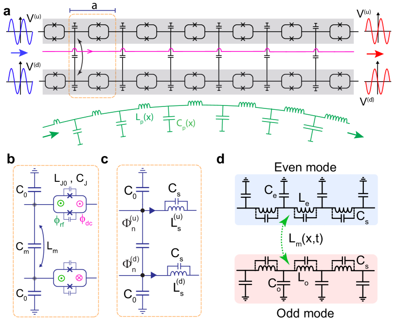
Implementation in superconducting circuit—Now, we proceed by discussing a practical implementation of this scheme in the superconducting circuit platform. The implementation has four essential components: I. Realizing two orthogonal modes of propagation (mode E and mode O) with distinct dispersion relations; II. Implementing the coupling between these two modes in a traveling wave fashion (Eq. 1); III. Carrying out the pump wave vector sweep (adiabatic phase matching) (Eq. 2); IV. And finally implementing the coupling strength variation (Eq. 3).
As depicted in Fig. 2a, we consider a pair of coupled lumped element transmission lines where the inductance in each unit-cell is provided predominantly by a pair of Josephson junctions in SQUID geometry. This forms a waveguide that supports two orthogonal modes of propagation; namely even and odd modes. The effective inductance of a SQUID is tuned by a dc bias line (shown in magenta) and also modulated by an rf pump in a separate transmission line (shown in green). We consider the configuration in which SQUIDs in the upper and lower lines receive dc flux in opposite directions while the rf flux modulations are in-phase for both lines as depicted in Fig. 2b. Therefore the effective inductance of SQUIDs in upper and lower transmission line would be,
| (5) |
where is the bare inductance of a single Josephson junction and is the reduced flux quantum and is the magnitude of the dc flux threading each SQUID. The rf flux has both temporal and spatial dependence inherited from the pump transmission line. We consider the regime where the signal currents propagating in the coupled transmission lines are much smaller than the critical current of the Josephson junctions (). In this regime, nonlinear effects due to signal propagation in the transmission lines are negligible. Therefore, SQUIDs can be considered as linear inductors whose inductance is modulated by (Fig. 2c). In the limit of small modulation, the effective inductance of SQUIDs in the upper and lower transmission line can be expressed as,
| (6) |
where the unitless parameter accounts for flux-pump-induced modulation and is the dc-biased SQUID inductance zorin2019flux .
The nonlinear dynamics of the system can be described by Lagrangian approach by defining node-fluxes in each transmission line yaakobi2013parametric ; zorin2019flux as depicted in Fig. 2c. However, we are interested in the dynamics of the even and odd modes corresponding respectively to symmetric and anti-symmetric node-flux superposition in the two transmission lines orfanidis2002electromagnetic . The equivalent circuit diagram in the even-odd basis is illustrated in Fig. 2d. Here , , and orfanidis2002electromagnetic ; supp . In this basis, we have two otherwise orthogonal propagation modes where an effective inductive mode coupling is induced by breaking the symmetry of upper and lower transmission lines via the rf flux. Far below the cut-off frequency of the transmission lines , and the Josephson plasma frequency , the even and odd modes’ characteristic impedance has the following form and the corresponding dispersion relations are,
| (7) |
In Fig. 1b, we plotted the dispersion curves for even/odd modes (blue/red lines) given a set of circuit parameters listed in Table 1. Note that the distinct dispersion relation for mode E and O is crucial for inhibiting the cascading parametric processes which otherwise would degrade the device performanceyu2009complete .
| Table 1: Circuit Parameters | |||
|---|---|---|---|
| fF | fF | fF | |
| pH | pH | ||
In the continuum limit where unit cell length is much smaller than the wavelength of propagating signals (), and far below the JJ plasma frequency, the dynamics of the node-flux in the even and odd modes can be described by a set of coupled PDEs supp ,
| (8) |
where we keep only the first order terms in and assume for brevity. Subscript and represent partial derivatives of time and position respectively. Here , where . We recast Eq. 8 in terms of forward/backward traveling waves in even and odd modes , where and and consider ansatze in form of , . Here we conveniently choose scaling parameters so that and are proportional to the average photon number propagating in each mode. For the induced coupling parameter, we consider where . Substituting these relations into the coupled equations (Eq. 8), and by applying the rotating wave approximations both in time and space 111Basically we ignore fast oscillatory terms either due to frequency mismatch or wavevector mismatch. With these approximations, forward and backward dynamics become effectively decoupled. In supplemental material supp (Fig. S3) we show that even with including higher oscillatory terms in the dynamical matrix we get similar result. and keeping only the first order terms in , we arrive at a coupled wave equations where and the dynamical matrix (see supplemental material for detailed derivations)
| (9) |
where the phase mismatches are defined as in Eq. 4. Here the effective coupling is
| (10) |
which is frequency dependent unlike our simple presented model (Eq. 4).
As illustrated in Fig. 2a, the spatially linear variation in pump wavevector is implemented by changing the capacitance and the inductance together in the pump transmission line as . In this way, the impedance of the line remains constant as . With the linear variation of the pump wavevector, the phase mismatch would be a linear function of position (See Eq. 2). We choose circuit parameters so that with pump frequency 2 GHz, perfect phase mismatching condition occurs at the center of the device for 6 GHz input signal which means in Eq. 2 we set , and for the pump wavevector sweep range we set which is reasonably achievable in practice.
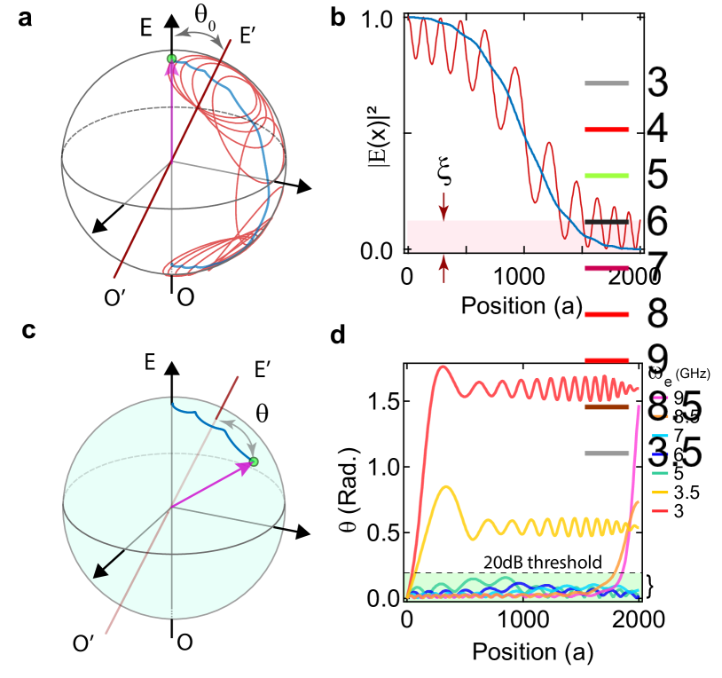
Now we discuss the implementation of spatial coupling strength ramp (Eq. 3) which is essential for this device to perform efficiently given practical limitations. The idea is that, to have an efficient adiabatic evolution, ideally, the system should start in an eigenmode and remain in its instantaneous eigenmode throughout the evolution. In our case, this requires that at the eigenmode of the system to be even/odd mode. Without spatial variation of coupling , the eigenmode of our system in the presence of flux drive would asymptotically approach to the even/odd mode in the limit of . However, due to practical upper-bound limitation for the pump maximum wavevector sweep range and lower-bound limitation for due to the finite device length, this requirement would not be met (in our case ). Therefore, as depicted in Fig. 3a and b, the signal starting at even mode at starts oscillating (the red path in 3a,b) and would not follow the ideal adiabatic path. The unwanted oscillation is translated to inefficient conversion at , which limits the isolation performance. However, increasing the mismatch sweep range is not the only way to ensure that the system starts in the eigenmode. One can slowly ramp off the coupling at both ends of the medium similar to pulse shaping techniques in the time domain martinis2014fast ; guerin2011optimal ; gambetta2011analytic ; yang2017achieving . With no coupling, mode E and O are eigenmodes and the signal starting at even mode at would not experience oscillatory evolution (e.g. the blue path in 3a,b). This technique of ramping the coupling drastically improves the adiabaticity of the evolution thus the efficiency of the conversion. In our model discussed earlier, we consider a quadratic scaling for effective coupling to carry out ramp up/down (Eq. 3). For the implementation we use slightly different ramping curve to partially compensate the frequency dependence of coupling (see Eq. 10). In our adiabatic scheme, since the effective coupling for different frequency happens effectively at different position, we can partially compensate for the frequency dependency of the coupling by implementing slightly stronger coupling at lower . We choose generalized Gaussian function,
| (11) |
where the parameter for and for controls the ramp up (ramp down) steepness. The parameters is a scaling factor to insure zero coupling at and maximum coupling at . Here corresponds to the maximum modulated inductance. The implemented ramp function is depicted in Fig. 1c inset (green curve). Practically, the ramping implementation can be done by varying the effective mutual coupling between pump line and SQUID loops as schematically illustrated in Fig. 2a.
Therefore, we have all essential components for the implementation of the proposed adiabatic scheme with a dynamics governed by Eq. (9). By terminating odd mode at both ends of the device (shown in Fig. 1a), and given the circuit parameters listed in Table 1, it gives more than 20 dB isolation over an octave of bandwidth as depicted in Fig. 1d (green curve).
adiabaticity analysis—We quantify the adiabaticity of the evolution by calculating the parameter which is the angle between the state of system (the magenta arrow in Fig. 3c) and the instantaneous eigenstate (red line in Fig. 3c) at any given position . Ideally in a full adiabatic evolution, is zero throughout the conversion which means system always follows its instantaneous eigenstate. In Fig. 3d we plot for different signal frequencies which stays close to zero for signals near 6 GHz and deviates significantly for 4 and 8 GHz as we expected from result in Fig. 1d. The angle at the end of the device determines the isolation as the probability of finding the signal at mode E at the end of the device is . The dashed line in Fig. 3d indicates the threshold angle below which we get more than 20 dB isolation. It is worth mentioning that, the final angle can be estimated by a simple geometrical analysis which is used for error estimation in adiabatic two qubit gates martinis2014fast ,
| (12) |
where and . For 20 dB isolation, the probability of the excitation at the end of the adiabatic evolution should be at most 1% () so should be less that 0.2 radian.
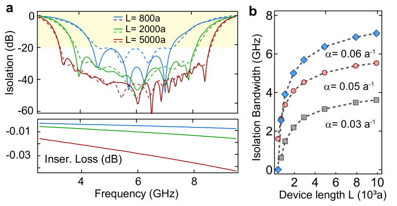
In Fig. 4a,we plot the isolation and transmission (insertion loss) performance for different device length (number of unit cells) given . Notably, the device with 800 unit cells provides over 2 GHz isolation bandwidth. The dashed lines are the estimated isolation using geometrical analysis (Eq. 12) which shows a great agreement with our result. The corresponding insertion loss plotted in the lower sub-panel in Fig. 4a is obtained by calculating the conversion of the mode E to mode O in backward direction and considering the typical dielectric loss in the superconducting qubit fabrications (loss tangent ). Figure 4c shows the isolation bandwidth versus the device length with given parameters in table 1 for three different mismatch sweep range . For infinitely long device the isolation approaches to the corresponding frequency range for pump wavevector sweep (e.g. for the isolation bandwidth approaches to GHz which is the highlighted frequency range in Fig. 1b).
mode splitter and impedance considerations— The impedance of the even and odd modes can be independently set by circuit parameters to the desired value. In this letter, we choose the parameters so that each transmission lines have 50 impedance. However, the impedance of the device is ultimately mandated by the termination configuration and the choice for the even/odd mode splitter at both ends of the device. For example, the odd mode can be blocked by a built-in broadband Wilkinson power divider. Alternatively one can use a broadband 180 hybrid couplers that split even and odd modes. The lumped element version of both types of terminations are readily available which can be naturally integrated with the device shen2009design ; gao2013design .
conclusion— Superconducting circuits have been shown a promising capability for realizing novel quantum devices. However, the realization of a large scale quantum system requires integration of its essential components. Here we show that nonlinear processes in coupled transmission lines open new possibilities of controlling photon dispersion and engineering novel quantum devices. We proposed a practical scheme for on-chip broadband isolator using adiabatic techniques and dispersion engineering in coupled superconducting transmission lines. The presented idea can be readily applied to other platforms such as silicon photonics.
acknowledgment— This work was funded in part by the AWS Center for Quantum Computing and by the MIT Research Support Committee from the NEC Corporation Fund for Research in Computers and Communications. Y. Ye acknowledges financial support from the MIT EECS Jin Au Kong fellowship. G. Cunningham acknowledges support from the Harvard Graduate School of Arts and Sciences Prize Fellowship.
References
- [1] Frank Arute, Kunal Arya, Ryan Babbush, Dave Bacon, Joseph C Bardin, Rami Barends, Rupak Biswas, Sergio Boixo, Fernando GSL Brandao, David A Buell, et al. Quantum supremacy using a programmable superconducting processor. Nature, 574(7779):505–510, 2019.
- [2] David M Pozar. Microwave engineering. John Wiley & Sons, 2009.
- [3] C. E. Fay and R. Comstock. Operation of the ferrite junction circulator. IEEE Transactions on Microwave Theory and Techniques, 13:15–27, 1965.
- [4] Quantum computing: progress and prospects. National Academies Press, 2019.
- [5] John Preskill. Reliable quantum computers. Proceedings of the Royal Society of London. Series A: Mathematical, Physical and Engineering Sciences, 454(1969):385–410, 1998.
- [6] Myeong Soo Kang, A Butsch, and P St J Russell. Reconfigurable light-driven opto-acoustic isolators in photonic crystal fibre. Nature Photonics, 5(9):549, 2011.
- [7] Shabir Barzanjeh, Matthias Wulf, Matilda Peruzzo, Mahmoud Kalaee, PB Dieterle, Oskar Painter, and Johannes M Fink. Mechanical on-chip microwave circulator. Nature communications, 8(1):1–7, 2017.
- [8] Hamidreza Ramezani, Tsampikos Kottos, Ramy El-Ganainy, and Demetrios N Christodoulides. Unidirectional nonlinear pt-symmetric optical structures. Physical Review A, 82(4):043803, 2010.
- [9] Nicholas Bender, Samuel Factor, Joshua D Bodyfelt, Hamidreza Ramezani, Demetrios N Christodoulides, Fred M Ellis, and Tsampikos Kottos. Observation of asymmetric transport in structures with active nonlinearities. Physical review letters, 110(23):234101, 2013.
- [10] Archana Kamal, John Clarke, and MH Devoret. Noiseless non-reciprocity in a parametric active device. Nature Physics, 7(4):311–315, 2011.
- [11] Benjamin J Chapman, Eric I Rosenthal, and KW Lehnert. Design of an on-chip superconducting microwave circulator with octave bandwidth. Physical Review Applied, 11(4):044048, 2019.
- [12] Benjamin J Chapman, Eric I Rosenthal, Joseph Kerckhoff, Bradley A Moores, Leila R Vale, JAB Mates, Gene C Hilton, Kevin Lalumiere, Alexandre Blais, and KW Lehnert. Widely tunable on-chip microwave circulator for superconducting quantum circuits. Physical Review X, 7(4):041043, 2017.
- [13] Leonardo Ranzani, Shlomi Kotler, Adam J Sirois, Michael P DeFeo, Manuel Castellanos-Beltran, Katarina Cicak, Leila R Vale, and José Aumentado. Wideband isolation by frequency conversion in a josephson-junction transmission line. Physical Review Applied, 8(5):054035, 2017.
- [14] Dimitrios L Sounas and Andrea Alù. Non-reciprocal photonics based on time modulation. Nature Photonics, 11(12):774–783, 2017.
- [15] Hermann A Haus and JA Mullen. Quantum noise in linear amplifiers. Physical Review, 128(5):2407, 1962.
- [16] Carlton M Caves. Quantum limits on noise in linear amplifiers. Physical Review D, 26(8):1817, 1982.
- [17] Aashish A Clerk, Michel H Devoret, Steven M Girvin, Florian Marquardt, and Robert J Schoelkopf. Introduction to quantum noise, measurement, and amplification. Reviews of Modern Physics, 82(2):1155, 2010.
- [18] Zongfu Yu and Shanhui Fan. Complete optical isolation created by indirect interband photonic transitions. Nature photonics, 3(2):91, 2009.
- [19] Hugo Lira, Zongfu Yu, Shanhui Fan, and Michal Lipson. Electrically driven nonreciprocity induced by interband photonic transition on a silicon chip. Physical review letters, 109(3):033901, 2012.
- [20] CR Doerr, L Chen, and D Vermeulen. Silicon photonics broadband modulation-based isolator. Optics express, 22(4):4493–4498, 2014.
- [21] Kevin O’Brien, Chris Macklin, Irfan Siddiqi, and Xiang Zhang. Resonant phase matching of josephson junction traveling wave parametric amplifiers. Physical review letters, 113(15):157001, 2014.
- [22] Haim Suchowski, Dan Oron, Ady Arie, and Yaron Silberberg. Geometrical representation of sum frequency generation and adiabatic frequency conversion. Physical Review A, 78(6):063821, 2008.
- [23] Haim Suchowski, Vaibhav Prabhudesai, Dan Oron, Ady Arie, and Yaron Silberberg. Robust adiabatic sum frequency conversion. Optics express, 17(15):12731–12740, 2009.
- [24] Haim Suchowski, Gil Porat, and Ady Arie. Adiabatic processes in frequency conversion. Laser & Photonics Reviews, 8(3):333–367, 2014.
- [25] William D Oliver, Yang Yu, Janice C Lee, Karl K Berggren, Leonid S Levitov, and Terry P Orlando. Mach-zehnder interferometry in a strongly driven superconducting qubit. Science, 310(5754):1653–1657, 2005.
- [26] Clarence Zener. Non-adiabatic crossing of energy levels. Proceedings of the Royal Society of London. Series A, Containing Papers of a Mathematical and Physical Character, 137(833):696–702, 1932.
- [27] Sergey N Shevchenko, Sahel Ashhab, and Franco Nori. Landau–zener–stückelberg interferometry. Physics Reports, 492(1):1–30, 2010.
- [28] JS Melinger, Suketu R Gandhi, A Hariharan, D Goswami, and WS Warren. Adiabatic population transfer with frequency-swept laser pulses. The Journal of chemical physics, 101(8):6439–6454, 1994.
- [29] Michael Garwood and Lance DelaBarre. The return of the frequency sweep: designing adiabatic pulses for contemporary nmr. Journal of magnetic resonance, 153(2):155–177, 2001.
- [30] Debabrata Goswami. Optical pulse shaping approaches to coherent control. Physics Reports, 374(6):385–481, 2003.
- [31] Yan-Xiong Du, Zhen-Tao Liang, Yi-Chao Li, Xian-Xian Yue, Qing-Xian Lv, Wei Huang, Xi Chen, Hui Yan, and Shi-Liang Zhu. Experimental realization of stimulated raman shortcut-to-adiabatic passage with cold atoms. Nature communications, 7(1):1–7, 2016.
- [32] John M Martinis and Michael R Geller. Fast adiabatic qubit gates using only z control. Physical Review A, 90(2):022307, 2014.
- [33] S Guérin, V Hakobyan, and HR Jauslin. Optimal adiabatic passage by shaped pulses: Efficiency and robustness. Physical Review A, 84(1):013423, 2011.
- [34] Jay M Gambetta, F Motzoi, ST Merkel, and Frank K Wilhelm. Analytic control methods for high-fidelity unitary operations in a weakly nonlinear oscillator. Physical Review A, 83(1):012308, 2011.
- [35] Yuan-Chi Yang, SN Coppersmith, and Mark Friesen. Achieving high-fidelity single-qubit gates in a strongly driven silicon-quantum-dot hybrid qubit. Physical Review A, 95(6):062321, 2017.
- [36] Aaron D O’Connell, M Ansmann, Radoslaw C Bialczak, Max Hofheinz, Nadav Katz, Erik Lucero, C McKenney, Matthew Neeley, Haohua Wang, Eva Maria Weig, et al. Microwave dielectric loss at single photon energies and millikelvin temperatures. Applied Physics Letters, 92(11):112903, 2008.
- [37] AB Zorin. Flux-driven josephson traveling-wave parametric amplifier. Physical Review Applied, 12(4):044051, 2019.
- [38] Oded Yaakobi, Lazar Friedland, Chris Macklin, and Irfan Siddiqi. Parametric amplification in josephson junction embedded transmission lines. Physical Review B, 87(14):144301, 2013.
- [39] Sophocles J Orfanidis. Electromagnetic waves and antennas. 2002.
- [40] Suplementary information.
- [41] Tze-Min Shen, Chin-Ren Chen, Ting-Yi Huang, and Ruey-Beei Wu. Design of lumped rat-race coupler in multilayer ltcc. In 2009 Asia Pacific Microwave Conference, pages 2120–2123. IEEE, 2009.
- [42] Nanjing Gao, Guoan Wu, and Qinghua Tang. Design of a novel compact dual-band wilkinson power divider with wide frequency ratio. IEEE Microwave and Wireless Components Letters, 24(2):81–83, 2013.