Imaging three phases of iodine on Ag (111) using low-temperature scanning tunneling microscopy
Abstract
We investigated the adsorption of iodine on Ag (111) in ultra-high vacuum. Using low-temperature scanning tunneling microscopy (LT-STM) measurements we catalog the complex surface structures on the local scale. We identified three distinct phases with increasing iodine coverage which we tentatively associate with three phases previously reported in LEED experiments (, , ). We used Fourier space and real space analysis to fully characterize each phase. While Fourier analysis most easily connects our measurements to previous LEED studies, the real space inspection reveals local variations in the superstructures of the and phase. The latter, observed here for the first time by LT-STM, appears to be stabilized by one or two adatoms sitting at the center of a rosette-like iodine reconstruction. The most stunning discovery is that variation in the adatom separation of the phase reconstructs the Ag (111) surface lattice.
I Introduction
Halogens on silver are of interest for catalytic purposes and for fundamental understanding of interaction of active gases with metal surfacesJones (1988); Andryushechkin et al. (2018). Furthermore, on-surface synthesis enables the formation of planar products and highly reactive substances that are inaccessible using traditional heterogeneous chemistry. To date, on-surface synthesis has focused on synthesizing carbon nanostructures from polycyclic hydrocarbons, with a large emphasis on using Ullmann-type reactions to couple organohalogens on metal surfaces such as Au, Ag and Cu. Held et al. (2017) The structure of the metal surface Ammon et al. (2019) and the pattern formed by self-assembly of the deposited precursors Grill et al. (2007) have both been shown to play a role in templating the nanostructure.
In the established on-surface Ullmann reactions, a high temperature anneal is required to activate the carbon–halogen bond and induce coupling of the pre-deposited precursors. This step also leaves a layer of halogen atoms on the substrate, which diffuses between the nanostructure and substrate resulting in both establishing a desirable electronic separation between the structure from the metal surface, and undesirably passivating the surface to further reaction. Eder et al. (2013) In fact, further work intentionally exposes the substrate post-reaction to additional iodine vapor to post-synthetically decouple the product from the substrate. Rastgoo-Lahrood et al. (2016)
A recent study overcomes the passivation challenge, by demonstrating that aryl coupling can be performed on a passivated surface, specifically an Ag(111) surface passivated with an inert chemisorbed iodine layer, by using an already activated aryl radical precursor in place of an aryl-halogen. Galeotti et al. (2020) The chemisorbed iodine layer was assumed to form the well-known hexagonal I-Ag(111) lattice.Andryushechkin et al. (2018). In this work, we demonstrate that the I-Ag(111) surface can be more complex than a single lattice structure. We show real-space STM images and analysis of three phases we associate with the three structures found by LEEDBardi and Rovida (1983); Yamada et al. (1996) with increasing coverage. To our knowledge, we present the first real-space images of the reconstruction. In light of observations that heating can transition the LEED pattern from to and backBardi and Rovida (1983) we discuss the possibility that the phase might be responsible for both phases. Through real space analysis of nearest-neighbor networks of the top monolayer as well as the superstructures we can relate the superstructure to the top iodine layer. In contrast, the superstructure is tied to the Ag (111) surface atoms. We further show that for either phase iodine can easily be manipulated by the STM tip. As the surface is known to play a role in templating Ullmann reactions, understanding the morphology of the passivating halogen layer is important for pursuing radical reactions on halogen passivated metal substrates.
II Experimental techniques
STM characterization was performed in a home-built low-temperature STM systemDreyer et al. (2010). In this system the bias voltage is applied to the sample while the tip is held at virtual ground by the transimpedance amplifier. The Ag (111) single crystal was cleaned in ultra-high vacuum (UHV) by cycles of argon ion etching at an energy of 750 eV while heating the sample to 450 ∘C as measured using an optical pyrometer. After the initial preparation, cleaning for minutes proved sufficient to refresh the surface. The surface quality was verified by measuring scanning tunneling spectroscopy (STS) maps of the Ag surface state where any contamination will act as a scattering center for the two dimensional electron gas. After cleaning, the sample was left to cool on the manipulator for 10 minutes prior to iodine exposure. The temperature was below the detection limit of our optical pyrometer of 250 ∘C, but was presumed to be above room temperature. Iodine was deposited from an AgI electrochemical cellFurman and Harrington (1996) at a rate of about ML/min. During the deposition the pressure inside the UHV chamber stayed in the low mbar range. Afterward, the sample was transferred into the STM and imaged at a temperature of 77 K – unless stated otherwise. For each iodine coverage the preparation process was repeated. During scanning iodine was randomly picked up by the tip which enhanced STM imaging.
III Results and discussion


The I/Ag(111) system has been extensively studied with electron diffraction techniques. Multiple phases have been identified with LEED, namely , , and Bardi and Rovida (1983); Yamada et al. (1996) which were observed with increasing iodine coverage. However, relatively few experiments have sought to identify the corresponding atomic structure for each of these phases with real space imaging techniques, such as STM. Some STM studies were performed in ambient conditionsSchott and White (1994); Hossick Schott and White (1994) as well as in ultra-high vacuumYamada et al. (1996); Bushell et al. (2005) and found the structure. One study described a “compressed ” structureAndryushechkin et al. (2018) which, we believe, is consistent with our images of the phase. For the phase there is broad agreement of iodine sitting in the FCC (ABCA …), not the HCP (ABA…), hollow sites of silver (111)Farrell et al. (1981); Maglietta et al. (1982); Forstmann et al. (1973). The atomic structure of the and phase have not been reported using STM.
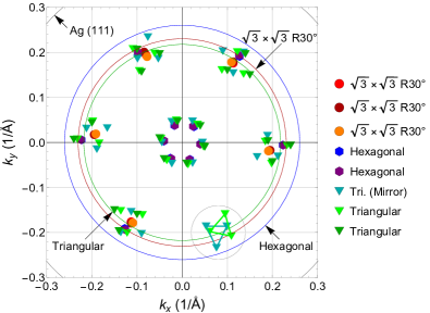
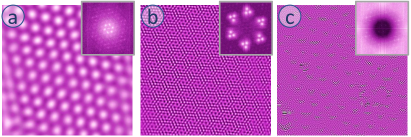
Figure 1 shows three representative STM images and the respective fast Fourier transformed (FFT) images which we associate with the three phases detected by LEEDBardi and Rovida (1983). The FFT images match the corresponding LEED patterns well. The measured length scales are also of the same order as the LEED observations. This can be seen in Fig. 2 and Tab. 1 which summarize the major FFT spots from eight different STM images. The FFT spots were rotated to compensate for the scan angle of the respective STM data set. The remaining differences in sample orientation are due to slight angle variations when locking the sample stud into the microscope. In particular the sample can be put into the microscope in two coarse orientations apart – usually at random. This, however, should not make any difference in FFT for the (111) surface of a cubic close-packed crystal such as Ag, the , , or structure. The structure, however, appears in FFT with two different orientations of the triangle spots. We attribute this to a mirrored reconstruction. We will discuss these mirror domains and their consequences later. The inner FFT peaks of the and phases represent a superstructure. While the orientation is similar, the periodicity of the two superstructures with Å and Å is clearly different (see App. C, Fig 17).
In addition to the FFT analysis we measured the individual atomic distances in real-space (See App. B). As shown in Tab. 1, the mean real-space distances reproduce the iodine-iodine distances () from FFT for the and phase. However for the phase we obtain the presumed FFT row-row distance () which is in excellent agreement with the published LEED values. This indicates that, in this case, FFT does not measure a row to row distance, as is expected for a triangular lattice, but rather the inter-atomic distance directly. This is likely due to the adatoms concealing part of the atomic lattice leaving mostly long stripes of the monolayer visible. The real-space measurements of the inter-atomic distances for the three reconstructions did not reveal any additional structure (See App. B). In contrast, real-space measurements of the and superstructures show substructures of their own (Section III.2).
| Reconstruction | LEED (Å) | FFT (Å) | RS (Å) | ||
|---|---|---|---|---|---|
| 5.00 | 4.43 | 4.88 | 5.64 | 5.79 | |
| 4.43 | 3.83 | 4.44 | 5.13 | 5.19 | |
| 4.59–5.00 | 3.98–4.43 | 4.82 | 5.57 | 4.87 | |
III.1 Up to ML ()


Figure 3 shows representative images of the reconstruction found at coverages of iodine up to ML. The images were taken at temperatures of (a) 77 K and (b) 4 K. Initially iodine is highly mobile at 77 K although it is difficult to distinguish between tip induced and thermal motion. Consequently, iodine is at first only visible as edge decoration. As the coverage approaches ML stable regions can be found on small Ag terraces. Larger terraces appear noisy due to the iodine motion. Even close to ML, where most areas show atomic order, some regions exhibit signs of motion as the patterns shift while scanning. One example is indicated by the ellipse in Fig. 3a). To the left of the defect the iodine lattice is intact while on the right side it appears distorted. The image also shows dark lines (arrow) which indicate tip changes where a presumed iodine atom at the tip apex gets pushed out of the way leading to a height change of Å. This is distinctly different from the iodine motion on the sample surface. Additionally, the tunneling current became increasingly noisy for bias voltages above V (applied to the sample) indicating tip induced iodine motion. No such effect exists for negative bias voltages.
In contrast, at 4 K (Fig. 3b), iodine forms stable areas even at coverages well below ML. Since the sample was prepared at room temperature, the ordering must occur while the sample is cooling down after being placed into the STM. Since such stable regions were not observed at 77 K, the iodine motion appears to freeze out between 77 K (6.6 meV) and 4 K (0.34 meV).
The phase has been observed multiple times by STM in different environmentsSchott and White (1994); Hossick Schott and White (1994); Yamada et al. (1996); Bushell et al. (2005). It shows no superstructure and has established iodine positions on Ag (111). However, the island structures found at a temperature of 4 K for the first time might deserve further study in terms of tip-induced iodine motion and the presumably size-dependent electronic structure.
III.2 and phases


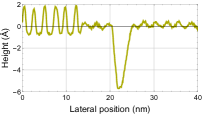
At coverages above ML we usually observed the coexistence of two reconstructions (phases) as shown in Fig. 4. No attempt was made to create a uniform coverage of either phase since it was not necessary for this STM study. The phase is preferentially found on the smaller terraces. The step edges remain straight with angles as is typical for a Ag (111) single crystal surface. Conversely, the phase is found on larger terraces with curved edges. This distinction allows one to identify either phase in larger STM scans that lack atomic resolution. Fig. 4b) shows one of the few cases where the phase grew up to the edge of a terrace covered by the phase. The expansion of the phase was likely hampered by a particle on the surface. The apparent step height between the two phases in Fig. 4b) varies nonlinear with bias voltage from Å to Å (See App. D.1, Fig. 20). This indicates, that the phase is more insulating than the phase.
III.2.1 phase


The structure has likely been observed before in STMAndryushechkin et al. (2018). As shown in Fig. 1c), the structure consists of atoms arranged in a triangular lattice with a Moiré like superstructure not unlike a charge density waveWilson et al. (1975). The interatomic distance between iodine atoms as measured by FFT was Å The superstructure had an average period of Å, while showing some irregularities in real space images. FFT also showed an average angle offset of between the atomic structure and the superstructure.
We separately determined the real-space lattice of the superstructure and the atomic structure (See App. A) from appropriately low-pass and high-pass filtered versions of three STM images obtained at different resolutions ( nm2, nm2, and nm2, each at pixels, App. D.1, Fig. 18). Higher resolution enhances the precision but limits the statistics, and vice versa. Fig. 5a) shows the combined histogram of the superstructure lattice constant. As expected, the mean value agrees well with the one determined by FFT. However, the histogram spreads over more than one iodine lattice constant which is wider than expected from noise. Another way to examine the lattice is to plot the distances from one maximum to its neighbors in a scatter plot (Fig. 5b). The plot shows mainly three blobs stemming from the three lattice directions. The blobs appear triangular in shape rather then ellipsoidal. The latter would be expected for a random shift caused by imaging noise as seen in Fig. 5b) for the atomic lattice of the phase. Examining the highest resolution data set separately (Fig. 6) sheds light on this structure. Here we find three distinct point groups at each of the three superlattice positions. The distance between the groups corresponds to the observed atomic distance within the surface and matches vectors of , and in the atomic lattice basis. We colorized the edges of the superstructure lattice according to the location in the scatter plot and overlaid it onto the STM image (Fig. 6). Here we find smaller “green”, larger “red” and rotated “orange” triangles as the main building blocks of the superlattice. The superlattice vertices are preferentially found between three surface atoms within a radius of 1.4 Å. This is more concisely shown in the appendix (App. D.1).
The structure becomes unstable at bias voltages V leading to pit formation when the STM tip repeatedly passes over an area. This allows one to measure a layer thickness of 6 Å. Cross sections also show a height change of Å from the to the phase (green). However, the measured heights vary with voltage (App. D.1, Fig. 20). This might indicate a reduced density of states of the phase and makes it difficult to ascertain the true layer thickness. It remains an open question whether Ag is mixing into the phase. Intermixing has been postulated for I/Ag(100) to explain a reconstruction observed on the (100) surfaceAndryushechkin et al. (2009). AgI can grow in a Wurtzite structure with a lattice constant of Å and Å. This form also has a band gap of eV in the bulk crystal. Since the dimensions are close to the observed values and we suspect a reduced density of states on this surface, AgI remains a possible candidate for the phase.
III.2.2 phase


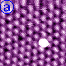
The phase is most peculiar. To our knowledge, no prior STM measurements of this phase have been reported. It consists of an iodine monolayer showing a rosette-like reconstruction with one or two adatoms sitting at the center of the each rosette. Fig. 7 shows an example across three terraces. The cross-section shows the normal step height of Ag (111) and an adatom height of about Å. On each terrace, the pattern of the iodine monolayer is atomically resolved all the way to the step edge. We note that the step edge is aligned with the reconstruction. The image also shows the rare occasion of an uncovered rosette structure in the lower right corner (yellow circle). The center appears brighter, likely due to an electronic effect that attracts the adatoms which we believe to be iodine. Selective FFT filtering identifies the rosette reconstruction as the source of the triangular spots in FFT while the six spots near the center represent the main components of the adatom structure (See App. F.1).
We performed a statistical analysis of the adatom structure over five images from two different sample preparations (details in App. F.3). We measured the ratio of singlets to doublets and analyzed the direction of the doublets. The results are summarized in Tab. 2. We found about of sites as singlets and as doublets. The ratio might depend on the coverage unless excess iodine is easily absorbed in the coexisting phase. The doublets are aligned in three distinct directions commensurate with the iodine monolayer. The distribution of the three possible angles was found to be approximately uniform.
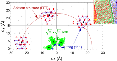
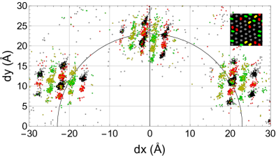
A closer examination reveals that the adatom lattice structure, and — by extension — the underlying rosette structure, is not very regular (Fig. 7a). We tested this by constructing a nearest neighbor network from the adatom centroid locations and separately from the positions of the iodine monolayer. Fig. 8 shows the edge distribution in a scatter plot. While the monolayer (green) shows a broad distribution without internal structure, the adatom distribution (red) was quite surprising. Instead of three somewhat broad spots for the three lattice directions we found three regions which resolve into a distinct triangular lattice of its own. Its average lattice constant is Å which is close to the atomic spacing of the Ag (111) surface ( Å) and distinct from the measured inter-iodine spacing of Å. Therefore the centers of the rosettes are tied to the Ag (111) lattice and not, as in the case of the phase, to the inter-iodine distance.
The mean lattice vector of the adatoms is close to in the Ag (111) basis (App. F, Fig. 29). This corresponds to a theoretical angle of between the Ag (111) surface vector and adatom lattice vectors which is close to the measured angle of . The structure and thereby possible correlations between superlattice vectors is obviously complicated since there are more than ten sub-spots for each direction. One correlation, however, concerns the double occupancy of adatom positions. It appears that the double occupancy preferentially occurs on distorted lattice sites, shifted by one Ag (111) lattice vector away from the most prominent adatom lattice position (App. F, Fig. 27). The shift also correlates with the orientation of the adatom dimer.


On a rare larger Ag terrace we found a mirror domain boundary of the phase. Mirror domains represent a change in chirality of the rosettes where the mean lattice vector should change from to in the Ag (111) basis. The expected angle between the domains is . Fig. 9 shows a sequence of zoomed in images of the domain boundary. The location of the boundary is marked in each image by a yellow arrow. The respective FFT (inset) show an average angle of between the respective adatom superstructures, close to the expected angle for two mirror domains. At the highest resolution (Fig. 9c) we find six spots in FFT (inset, yellow circle) for the underlying rosette reconstruction of the iodine monolayer. As shown in Fig. 10, the spots are the composition of two opposing triangles from the left and right side of the domain boundary (cf. Fig. 2). This immediately raises the question whether the LEED patterns of the phase is merely the average over multiple domains. We found, however, that mixed domains are only allowed on larger terraces and that the chirality is tied to the mean direction of the underlying Ag steps. The linkage was confirmed in an area where the step direction changed by and the FFT image showed split adatom peaks (App. F.2, Fig. 24). Selective filtering ties the chirality of the domains to the respective step direction. A forcing effect then might result from the average orientation of the Ag step edges with respect to the Ag crystal lattice which is also given by the misorientation of the surface with respect to the (111) normal with the azimuth component defining the average step orientation. Given that for an angle of the average width of the Ag terraces is only Å nm we assume that the LEED experiments would show a single domain and hence a triangular structure. This proposed coupling of the prevalent step direction of the single crystal to the chirality of the iodine reconstruction might serve as an explanation of the LEED results.


The mirror domains allow deeper insight into the alignment of the rosette reconstruction with the Ag (111) surface atoms. We separately constructed the adatom lattice for either domain and plotted the edge distribution in Fig. 11. The edge distribution shows two distinct sets of interwoven triangular lattices, each similar to the one shown in Fig. 8. Extracting the edge distribution from the interwoven lattice leads to three spots in a scatter plot at the Ag lattice constant, confirming a single underlying Ag lattice as expected. The interwoven nature of the edge distributions requires the rosette centers to sit on Ag (111) hollow sites. This is shown in more detail in appendix F (Fig. 28). Mirroring the edge distribution from one domain at an angle of (the angle offset found for the adatom structure in FFT) leads to overlapping point groups — even with a similar structure. This confirms that the two domains are indeed of the same structure. Fig. 11 also shows that the mirror plane (black line) runs along one of the Ag (111) lattice vectors.


Finally, the adatom structure can be disturbed by the STM tip. Fig. 12a) shows the result of a single V pulse applied to the STM junction. The adatom structure was altered within a radius of nm of the tip position. Outside the radius, the regular adatom structure remained. A closer inspection of the exposed iodine monolayer (Fig. 12b) does not show the expected rosette pattern. Instead, a slightly wavy superstructure of the monolayer, which was stable over multiple scans, is now visible. This raises the question whether the adatom structure is necessary to stabilize the structure, or whether the pulse was disruptive enough to also disturb the rosette reconstruction of the monolayer. In a different region we inadvertently removed part of the adatoms while taking an STS map (Fig. 22a). This also led to a local change of the rosette pattern. We therefore assume that the adatoms are integral to the structure.
IV Conclusion
We observed three phases of iodine on silver (111) using low temperature STM which tentatively match the , , and phases found in early LEED experiments. The phase shows the worst match in terms of lattice constant compared to LEED.
The main findings for the three phases are:
-
At 77 K, iodine is highly mobile until the full coverage is reached. Step edges stabilize the motion. We found no superstructure. At 4 K iodine mobility is reduced and we find stable islands or holes in the iodine layer depending on coverage.
-
This structure, found on larger terraces, could be a double layer of iodine or the onset of AgI growth. It shows a charge-density-wave-like superstructure with maxima located at hollow sites of the top layer atoms. The distance of the superstructure maxima corresponds to 4 or 5 atomic distances, respectively, leading to a somewhat disordered appearance. Atoms can easily be removed by voltage pulses and larger vacancies formed this way distort the superstructure.
-
This is the most intriguing structure. Iodine forms a mosaic of rosettes which apparently are stabilized by one or two adatoms at the center of each rosette. Removing the adatoms over larger areas with the STM tip also destroys the rosette structure. The adatom positions and, by extension, the centers of the rosettes are aligned with hollow sites of the underlying Ag lattice. The vectors of the adatom lattice vary by lattice vectors of the silver surface. The chirality of the rosettes is bound to the predominant Ag step direction. The latter is given by the miss-cut of the Ag crystal and thus varies little on well prepared surfaces. This explains why a triangular pattern is observed in LEED studies where small domains of random chirality would lead to a hexagonal appearance.
References
- Jones (1988) R. G. Jones, Progress in Surface Science 27, 25 (1988).
- Andryushechkin et al. (2018) B. Andryushechkin, T. Pavlova, and K. Eltsov, Surface Science Reports 73, 83 (2018).
- Held et al. (2017) P. A. Held, H. Fuchs, and A. Studer, Chemistry – A European Journal 23, 5874 (2017).
- Ammon et al. (2019) M. Ammon, M. Haller, S. Sorayya, and S. Maier, ChemPhysChem 20, 2333 (2019).
- Grill et al. (2007) L. Grill, M. Dyer, L. Lafferentz, M. Persson, M. V. Peters, and S. Hecht, Nature Nanotechnology 2, 687 (2007).
- Eder et al. (2013) G. Eder, E. F. Smith, I. Cebula, W. M. Heckl, P. H. Beton, and M. Lackinger, ACS Nano 7, 3014 (2013).
- Rastgoo-Lahrood et al. (2016) A. Rastgoo-Lahrood, J. Björk, M. Lischka, J. Eichhorn, S. Kloft, M. Fritton, T. Strunskus, D. Samanta, M. Schmittel, W. M. Heckl, and M. Lackinger, Angewandte Chemie International Edition 55, 7650 (2016).
- Galeotti et al. (2020) G. Galeotti, M. Fritton, and M. Lackinger, Angewandte Chemie International Edition 59, 22785 (2020).
- Bardi and Rovida (1983) U. Bardi and G. Rovida, Surface Science 128, 145 (1983).
- Yamada et al. (1996) T. Yamada, K. Ogaki, S. Okubo, and K. Itaya, Surface Science 369, 321 (1996).
- Dreyer et al. (2010) M. Dreyer, J. Lee, H. Wang, and B. Barker, Review of Scientific Instruments 81, 053703 (2010).
- Furman and Harrington (1996) S. A. Furman and D. A. Harrington, Journal of Vacuum Science & Technology A 14, 256 (1996).
- Schott and White (1994) J. H. Schott and H. S. White, The Journal of Physical Chemistry 98, 291 (1994), https://doi.org/10.1021/j100052a049 .
- Hossick Schott and White (1994) J. Hossick Schott and H. S. White, Langmuir 10, 486 (1994), https://doi.org/10.1021/la00014a024 .
- Bushell et al. (2005) J. Bushell, A. F. Carley, M. Coughlin, P. R. Davies, D. Edwards, D. J. Morgan, and M. Parsons, The Journal of Physical Chemistry B 109, 9556 (2005), pMID: 16852150, https://doi.org/10.1021/jp0513465 .
- Farrell et al. (1981) H. Farrell, M. Traum, N. Smith, W. Royer, D. Woodruff, and P. Johnson, Surface Science 102, 527 (1981).
- Maglietta et al. (1982) M. Maglietta, E. Zanazzi, U. Bardi, D. Sondericker, F. Jona, and P. Marcus, Surface Science 123, 141 (1982).
- Forstmann et al. (1973) F. Forstmann, W. Berndt, and P. Büttner, Phys. Rev. Lett. 30, 17 (1973).
- Wilson et al. (1975) J. Wilson, F. D. Salvo, and S. Mahajan, Advances in Physics 24, 117 (1975).
- Andryushechkin et al. (2009) B. V. Andryushechkin, G. M. Zhidomirov, K. N. Eltsov, Y. V. Hladchanka, and A. A. Korlyukov, Phys. Rev. B 80, 125409 (2009).
Appendix A Real-space analysis
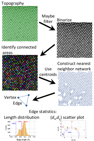
Analyzing lattices in real space allows one to detect and classify local changes in lattice parameters and to identify systematic variations. Furthermore, relations between the atomic lattice and a superstructure can be evaluated at the local level. The process is shown in Fig. 13. We started with an STM data set. The data was sometimes filtered to eliminate steps or to separate the atomic structure from a superstructure. In general, preprocessing was applied as sparingly as possible to avoid the possible introduction of artifacts. The data was then binarized with a chosen threshold level resulting in well separated cohesive regions. For each of the regions the centroid position, area, and sometimes elongation were extracted. Using the centroids positions was sufficiently accurate. More sophisticated approaches, such as using the topographic data as weights when calculating the centroids, gave little or no improvement. The results were post-selected based on area to eliminate spurious features due to noise or residual step edges. The centroid positions were then used as vertices to generate a nearest neighbor network graph, typically with six neighbors assuming a triangular lattice. Again, post-selection was used to exclude graph edges that were clearly too long or too short. Other defects such as crossing graph edges were left in place. These defects were rare enough to remain statistically insignificant. Throughout the process all back references were maintained to identify the source of any anomaly within the original STM data. The distribution of the edge length typically had a mean value close to the lattice constant determined by FFT, while a histogram width and shape give hints as to the existence of substructures. A second instructive visualization was to mark each edge vector directly in a scatter plot. For a regular triangular lattice we expect three ellipsoidal clusters. The size and asymmetry of a cluster are due to imaging noise and scanner distortions, respectively. Clusters at combinations of lattice vectors stem from missing or missed nearest neighbors so that next-nearest neighbors were included during the graph construction. Similarly, single points were errors most likely from binarizing the image creating spurious connected regions. In contrast, clusters at positions incommensurate with the expected lattice vector hint at a physical cause. This is the case for the and superstructure.
Appendix B Supplemental: real-space measurements of the interatomic distances


We measured the inter-atomic distances while disregarding any existing superstructure for the three phases of iodine on Ag (111) by appropriately filtering the images. After finding the atom locations we constructed a nearest neighbor graph with a maximum of six neighbors within a cut-off radius of Å, but no further restraints. The histogram in Fig. 14–16 shows the length distribution of the respective graph edges. As expected, the mean value of the distribution agrees with the value measured by FFT. The multiple peaks are likely an artifact of the STM measurement due to the x-y asymmetry of the piezo scanner. Using the x and y distances of all graph edges we generated the respective scatter plot. The three main spots represent the primary axis of the triangular lattice. They appear just as elliptical structureless blobs. The respective centroids give us the atomic lattice vectors.
Appendix C FFT peaks of the and superlattice structure
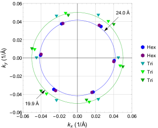
Figure 17 shows an enlarged version of the inner FFT spots from Fig. 2 representing the superstructure of the and phase. We found clearly different average length scales of Å and Å respectively. The clear difference points to different superstructure origins. The angular distribution is somewhat similar likely linked to the underlying Ag (111) surface.
Appendix D Supplemental
D.1 superlattice structure


We determined the relative position of the superlattice maxima (SLM) with respect to the atomic lattice of the phase. For each of the SLM within three STM images (see Fig. 18) we determined the location of the three nearest surface atoms. From the three locations we calculated the respective center and the distance to the SLM. The scatter plot in Fig. 19 shows the surface atom locations in red and the SLM in blue. The locations are aligned by subtracting the respective from both the SLM position as well as the three atom positions. It is obvious that while the SLM location shows some scatter it lies mostly near the center of the three surrounding atoms. The histograms show the probability density function of the SLM distance from the center estimated by a gamma distribution .


The apparent step height from the to the reconstruction varies from 0.7 Å at low absolute bias voltage to 2.5 Å at bias voltages V (Fig. 4). This indicates that the phase is more insulating than the phase.
Appendix E Tip induced modifications


The structure becomes unstable at bias voltages V leading to pit formation when the STM tip repeatedly passes over an area. Two examples are shown in Fig. 22 along with cross sections. Fig. 22a) shows a subset of the area shown in Fig. 4b). The adatoms of the phase have been disturbed after taking a spectroscopic map in the area with a voltage range of V. Topographic imaging at these voltages usually leaves the atomic structure unperturbed. The phase was not disturbed by the STS measurement but subsequently modified by repeated imaging of a small area at V. The cross sections show a height change of Å from the to the phase (green). The step height measurement varies with voltage (App. D.1, Fig. 20). This might indicate a reduced density of states of the phase and makes it difficult to ascertain the layer thickness. The yellow cross section shows a corrugation of Å for the phase. The hole shows a depth of about Å, but without a clear flat bottom. In a second area (Fig. 22b) we repeated the process to create a larger hole. Here the cross section clearly shows a flat bottom and a depth of Å with a shelf at Å. The later might be due to a double tip artifact. It is also noteworthy that in this case the superstructure showed distortions while for the smaller hole in Fig. 22a) the superstructure remained intact. Also, in both cases, the phase is atomically resolved up to the edges of the holes as well as at the boundary with the phase in Fig. 22a).
Appendix F Supplemental
F.1 Selective FFT filtering
FFT filtering allows one to easily correlate peaks in the FFT spectrum to topographic features. Fig. 23 shows an example for the structure as filtered real space images together with its FFT after applying the respective filter. The inner spots in FFT (a) clearly belong to the superstructure, although the double occupancy at certain sites is lost. Filtering on the FFT peaks (b) leaves the visible iodine monolayer showing the outer rosette structure. The center portion remains diffuse since it was covered up by the adatoms and thus cannot be reconstructed by inverse FFT. Finally, high-pass filtering with a cutoff length scale of Å shows noisy features near the adatom position. This is the residual effect of variations of the adatom positions on the Ag (111) lattice.
F.2 domains bound to step edge


Figure 24a) shows a stepped area with two mirror domains. We used FFT filtering to highlight either domain, shown in Fig. 24b) and c). The estimated domain boundary is marked with a yellow line with an inscribed angle of . The green line marks the estimated change in step direction of . Comparing the domain boundary to the Ag (111) step direction in Fig. 24a) a linkage becomes apparent as the domain boundary (yellow) also demarcates the Ag (111) step domains.
F.3 Semi-automatic Adatom Classification
| data set | Total | single | double | ang1 | ang2 | ang3 | ||||||
|---|---|---|---|---|---|---|---|---|---|---|---|---|
| 1 | 165 | 62.4 % | 37.6 % |
|
|
|
||||||
| 2 | 1795 | 58.4 % | 41.6 % |
|
|
|
||||||
| 3 | 1849 | 70.4 % | 29.6 % |
|
|
|
||||||
| 4 | 2163 | 65.0 % | 35.0 % |
|
|
|
||||||
| 91008A06.tfr 5 | 517 | 66.2 % | 33.8 % |
|
|
|


We used Mathematica to identify and classify the adatoms found on the phase. An example is shown in Fig. 25. The image was filter followed by binarization and extractions of cohesive areas. From areas above a pixel threshold of typically 5 we extracted the centroid position as well as other parameters such as area (). The elongation () and angle of the long axis () where determined by a fit to an equal-area ellipse. Fig. 25 shows polar plots of and . The latter was used to distinguish between single or double occupancy and to classify for the adatom dimers. The angle of the dimers lies in three direction of the direction of the Ag (111) with a seemingly random distribution. The estimated inter-dimer distance was 7.7 Å. All real space measurements followed this scheme. The filter function and binarization threshold had to be adapted for the respective data set.


For a deeper analysis we colored the edges of the adatom nearest neighbor network according to their length, similar to what we did for the phase shown in Fig. 6. The result is shown in Fig. 26. The three regions in the NNN edge distribution plot were overlapped by rotating them by an angle of and degrees, respectively. However, since there are up to 15 different length scales to consider (the example shows coloring for just 6), this method is of limited use.
Some insight could be gained by finding the distances involving dimer-occupied sites. Fig. 27 shows an example. The points in the NNN distance vector plot of the adatom lattice are colored if they involve a dimer site. The colors are chosen according to the major axis angle (see inset). This distinguishes the cluster points and hints at a coupling of the occupancy number and dimer orientation to the local strain build into the iodine monolayer.


The mirror domains (Fig. 9) allow to locate the center of the rosettes on Ag (111) hollow sites. First, the distances within the NNN distance vector plots of the adatoms for both domains give three base vectors for a single Ag (111) surface (Fig. 28, top). Selecting two base vectors we can reconstruct the Ag (111) lattice including the x-y piezo asymmetry due to piezo creep. Overlaying the adatom NNN vector distribution shows hollow sites as a plausible location for the rosette centers.


Figure 29 shows a simple model for the rosette centers of the phase. The blue points mark Ag (111) locations and the red points mark a lattice — the average lattice vector for the adatoms. The lower figure demonstrates that a simple can not maintain hollow sites consistently. Therefore local distortions are expected.