Area-selective deposition and B -doping of Si(100) with BCl3
Abstract
B-doped -layers were fabricated in Si(100) using BCl3 as a dopant precursor in ultrahigh vacuum. BCl3 adsorbed readily at room temperature, as revealed by scanning tunneling microscopy (STM) imaging. Annealing at elevated temperatures facilitated B incorporation into the Si substrate. Secondary ion mass spectrometry (SIMS) depth profiling demonstrated a peak B concentration 1.2(1) 1021 cm-3 with a total areal dose of 1.85(1) 1014 cm-2 resulting from a 30 L BCl3 dose at 150 ∘C. Hall bar measurements of a similar sample were performed at 3.0 K revealing a sheet resistance of = 1.91 k, a hole concentration of = 1.90 1014 cm-2 and a hole mobility of = 38.0 cm2V-1s-1 without performing an incorporation anneal. Further, the conductivity of several B-doped -layers showed a log dependence on temperature suggestive of a two-dimensional system. Selective-area deposition of BCl3 was also demonstrated using both H- and Cl-based monatomic resists. In comparison to a dosed area on bare Si, adsorption selectivity ratios for H and Cl resists were determined by SIMS to be 310(10):1 and 1529(5):1, respectively, further validating the use of BCl3 as a dopant precursor for atomic precision fabrication of acceptor-doped devices in Si.
I Introduction
The realization of atomic-precision, advanced manufacturing (APAM) processes using acceptor and donor doping is an essential step towards integrated quantum circuitriesWard et al. (2020). APAM process development, thus far, has largely focused on donor dopant-based devices in Si, and in particular, the precision placement of P atoms and their subsequent operation as qubitsWeber et al. (2014). More recently, acceptor-based Si devices have been proposedSalfi et al. (2014, 2016); Shim and Tahan (2014); Blase et al. (2009) and realizedŠkereň et al. (2020) demonstrating the opportunities of hole-type devices and the need for further development of alternate chemistries for device fabrication. While APAM acceptor-doped devices have been demonstrated in Si(100) using diborane (B2H6)Škereň et al. (2020), it results in the formation of electrically inactive dopant complexes due to its inherent dimerized natureCampbell et al. (2021), prompting further investigations towards finding a more ideally suited B dopant precursor.
The use of BCl3 as a dopant precursor has been well documented on Si substratesHerner and Clark (2004); Consiglio et al. (2016); Pilli et al. (2018); Duvauchelle et al. (2015). Moreover, it has been used to achieve superconductivity in Si through gas immersion laser dopingCammilleri et al. (2008). While these BCl3 doping demonstrations have all been performed at temperatures or processing conditions that are inherently incompatible with the current APAM process flow, they remain suggestive of the potential viability of BCl3 as an APAM acceptor precursor that warrants further investigation.
In this paper, we demonstrate the formation and characterization of B-doped -layers from BCl3-dosed Si(100). We find that BCl3 adsorbs readily onto the Si(100) surface at room temperature. Further, the adsorption of BCl3 generates an active carrier concentration exceeding 1014 cm-2 without directly annealing the substrate to facilitate activation. STM was used to verify both BCl3 adsorption and B incorporation, while secondary ion mass spectrometry (SIMS) depth profiling was used to quantify the B content of the -layers and verify resist selectivity. We find BCl3 to demonstrate selectivity in adsorption on H- and Cl-terminated Si with respect to bare Si(100), making it chemically compatible with current STM lithographic processes. Hall bar measurements obtained at 3.0 K revealed similar values for sheet resistance, carrier concentration, and carrier mobility to those reported for the well developed process of P-doped -layers formation using PH3. This work serves as a stepping stone to enable further development of acceptor-based devices, including complementary digital electronics at the atomic-scale.
II Experimental Methods
II.1 B -Layer Preparation
BCl3 dosing, STM imaging, and lithography were performed in a ScientaOmicron VT-STM ultra-high vacuum (UHV) system with base pressure Pa ( Torr). The STM is run using a ZyVector STM Lithography control system. The Si(100) wafers used in these experiments were p-type (B-doped) obtained from ITME with resistivity = 1 cm to 10 cm, and oriented within 0.5∘ of (100). Si samples used for dosing tests and electrical measurements were cut to 4 mm 12 mm in size and cleaned by sonication in acetone, methanol, and isopropanol. Samples were then immediately mounted on a ScientaOmicron XA sample plate and loaded into the UHV system. Samples used for lithography tests were prepared differently. Fiducial marks were etched in the surface to allow a patterned area to be relocated in the STM (see Supplemental Information). These samples were then diced to 5 mm 9 mm and chemically cleaned of metals and organics using a common cleaning recipe consisting of piranha solution (H2SO4:H2O2), HF, and SC-2 (H2O:HCl:H2O2) before being sonicated and loaded in a similar manner to other samples. Clean Si(100)-(21) surfaces were prepared in UHV following the procedure described in Ref. Trenhaile et al., 2006 by flash annealing the sample to 1225 ∘C. Sample temperature was monitored with an optical pyrometer. Each sample was initially scanned in the STM to check that it was free of metal and carbon contaminants then re-flashed to produce a fresh Si(100) surface prior to BCl3 dosing.
Samples were generally slightly above room temperature during sample transfer to the dosing chamber and BCl3 dosing to minimize water contaminationYu et al. (2008) and, ultimately, O content within the B -layer. BCl3 was introduced into the UHV chamber via a precision leak valve with dosing pressures ranging from 1.3 Pa ( Torr) and 5.3 Pa ( Torr). Dosing values reported here are expressed in units of Langmuir (1 L = 10-6 Torrs) and generally have a relative uncertainty of 0.1. Dosing parameters were varied for three samples used for electrical measurements, denoted samples B2, B3, and B4. Sample B2 was dosed with 3.6 L BCl3 at room temperature (20 ∘C), sample B3 was dosed with 3.6 L BCl3 at 350 ∘C to try to drive chemisorption and increase the B concentration beyond the room temperature saturation, and sample B4 was dosed with 0.12 L BCl3 at room temperature (20 ∘C). B incorporation anneals were not performed on these samples. Another sample used for SIMS analysis, denoted B1, was dosed with 30 L BCl3 at 150 ∘C to prevent any water adsorption then annealed at 350 ∘C to incorporate the B. To form buried B -layers and enable ex situ SIMS and electrical measurements, BCl3-dosed samples were encapsulated with 20 nm to 65 nm of Si at a typical rate of 0.016 nm/s using a MBE Komponenten SUSI-63 sublimation source. Samples B1 and B4 was encapsulated with a deposition rate of 0.004 nm/s at 240 ∘C. Other samples were not heated deliberately during deposition, although thermal radiation from the deposition source heated the sample to around 200 ∘C to 250 ∘C. SIMS depth profiling (Eurofins EAG Materials Science) was used to quantify the B, Cl, and H content of the B -layers and Si films.
II.2 Electrical Measurements
Electrical transport properties of the B -layers were characterized with standard Hall bar measurements. Hall bars of width 25 m and length 60 m were patterned by electron beam lithography and the surrounding area was etched to a depth of around 100 nm with a reactive ion etcher (RIE) (see Supplemental Information). A 50 50 array of 1 m sized squares were also etched into the contact pad region to enhance the contact quality between each pad and the B-doped -layer. Ti/Au (5 nm/150 nm) was then deposited using an electron-beam deposition system to define the contact pads. Through this method, contact resistances of 1 k at room temperature were routinely achieved without any annealing process. Electrical transport measurements of the B -layers were performed at temperatures ranging from 300 K to 1.9 K and magnetic fields from -14 T to +14 T to characterize the sheet resistance (), hole carrier density (), and mobility (). The values for these parameters reported here were measured at 3.0 K, where the measurement system was more stable.
III Results and Discussion
III.1 BCl3 Adsorption and Incorporation
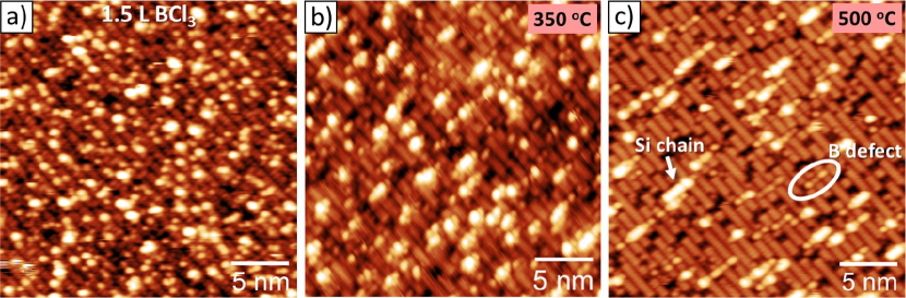
Density functional theory calculations have determined that BCl3 dissociatively chemisorbs onto Si(100) forming Si-BCl2 and Si-Cl moieties on a single Si dimerFerguson et al. (2009). There are a number of papers discussing the use of BCl3 as a dopant sourceDeutsch et al. (1981); Kunii et al. (2004), and there have also been a number of investigations of adsorption on Si(111)Lapiano-Smith and McFeely (1992), but to the best of our knowledge, no STM studies exist of BCl3 adsorption on the Si(100) surface. Figure 1 shows filled-state STM images of a Si(100) surface exposed to BCl3 before (a) and after annealing to 350 ∘C (b) or 500 ∘C (c). The surface was dosed with 1.5 L of BCl3 at room temperature (20 ∘C) resulting in numerous bright features due to adsorbates as seen in Fig. 1(a). BCl3 is widely used in ALD applications and is known to stick readily to Si(100)Pilli et al. (2018); Consiglio et al. (2016); Ferguson et al. (2002). We also find BCl3 to adsorb readily onto the Si(100) surface at room temperature forming a variety of surface bound structures. Many of these features are likely chemisorbed BCl2 and as well as Cl atoms. The brighter BCl3 features in (a) comprise a surface coverage of roughly 0.32.
After dosing, several samples were annealed at different temperatures to observe the evolution of surface features with temperature, eventually leading to incorporation of the B atoms into the substrate, which is typically done to foster electrical activation. Figure 1(b) depicts the surface of a sample with the same dose as in (a) after annealing at 350 ∘C for 1 minute. Some of the smaller round BCl3 adsorbate features seen in (a) are gone while larger features remain. This may indicate partial dissociation or incorporation into the surface at this temperature. Also seen are darker dimer row defects, which can indicate additional Cl on the surface.
Figure 1(c) depicts the surface shown in (a) after annealing at 500 ∘C for 1 minute. This anneal was chosen based on similar anneals used for B2H6 Škereň et al. (2020) and AlCl3 incorporationRadue et al. (2021). The annealed surface appears quite differently with many of the bright round features in (a) disappearing. Short Si chains running perpendicular to the underlying dimer row direction can be seen on the surface (arrow) with their height verified to be one atomic layer. This is a potential indicator that B atoms were incorporated into the surface causing Si atoms to be ejected as adatoms, forming the chains. It is also possible that some of the ejected Si observed was the result of surface etching due to the presence of Cl on the surface during the anneal step. Very little Cl is observed on the annealed surface in Fig. 1(c), matching our expectation that Cl is removed at 500 ∘CRadue et al. (2021). Additionally, among the various defects that are visible, there appears to be B-related surface defects (circle) which span three dimer rows and are similar to features often observed on B-doped Si substrates caused by B atoms several layers below the surfaceLiu et al. (2008); Wang and Hamers (1995). Annealing at intermediate temperatures of 400 ∘C and 450 ∘C produce similar surfaces to the 350 ∘C surface in Fig. 1(b), though with additional Si chains appearing at 450 ∘C, indicating that this temperature is closer to the onset of B incorporation.
III.2 SIMS Characterization of B -Layers
As discussed earlier, B -doped samples were formed by exposing clean Si(100) to BCl3 and then capping them with epitaxial Si. The -layers were characterized ex situ with SIMS to ascertain the estimated peak dopant concentration, the areal dose, and the estimated thickness of the -doped layer. Figure 2 shows SIMS depth profiles of -layer samples B1 and B2. Sample B1 was capped with 19 nm Si and B2 was capped with 62 nm Si after dosing. B profiles show in Fig. 2 represent the total B, i.e. the sum of 10B and 11B. For B2 (dotted line), the peak B concentration was measured to be 4.1(1) 1020 cm-3 at the interface with a total areal dose of 1.59(1) 1014 cm-2. While the SIMS measurement for B2 was performed using typical settings, -layer sample B1 was measured using a lower primary ion energy of 250 eV resulting in a higher spacial resolution. The measurement on B1 was done as a reference to more accurately gauge the peak B concentration and, importantly, the -layer thickness when eliminating some known SIMS measurement artifactsGautier et al. (1996). Areal dose accuracy, however, is consistent between different measurement types, according to the analysis provider. We believe the 3.6 L dose of B2 is at or near a saturation dose and thus the higher 30 L dose of B1 should not lead to a significantly increased B content. The high resolution measurement of B1 yielded a peak B concentration of 1.2(1) 1021 cm-3 with a total areal dose of 1.85(1) 1014 cm-2, similar to the areal dose of B2. Additionally, a SIMS measurement of B1 using a primary ion energy of 1 keV, similar to that of B2, shows a significant lowering of the peak to 6.3(1) 1020 cm-3 (see Supplemental Information). It can therefore be assumed that the peak B concentration for sample B2 used in electrical measurements is closer to 1021 cm-3 than that measurement indicated. This B concentration is similar to reported concentrations for B and P -layers deposited via a precursor of roughly 1021 cm-3, and the areal dose is similar for PHagmann et al. (2018); Škereň et al. (2020). It is also consistent with a number of reported B-doped -layers fabricated using molecular beam epitaxy (MBE)Weir et al. (1994).
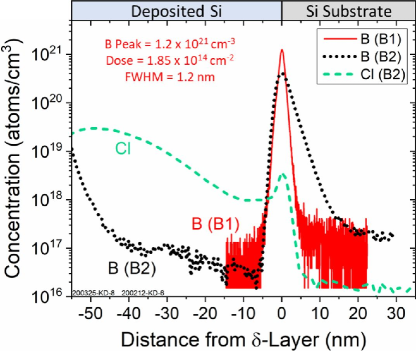
One measure of the thickness of the -layers is determined from the full width at half max (FWHM) of the B peak in Fig. 2. For sample B1, the thickness of the B -layer is estimated from the displayed depth profile to be 1.2 nm. This value is close to the measurement limit of SIMS even using high resolution settings and so may yet be an overestimate. The lower resolution measurement of sample B2 resulted in a FWHM of 3.4 nm. However, by comparing the SIMS data from multiple measurement energies, a measure of the SIMS instrument artifacts that cause broadening of the -layer can be determinedGautier et al. (1996). Then, an estimate of the “true” thickness can be extrapolated for a situation with zero instrument artifact effects (see Supplemental Information). Extrapolating the measurements from sample B1 in this manner yielded a FWHM of 0.8 nm. Further, by fitting the depth profiles at each energy to a -layer model that accounts for the instrument broadening, the standard deviation on the distribution of B can also be extrapolated to reduce the broadening effect. This type of analysis was done for sample B1 and resulted in a standard deviation of the -layer thickness of 0.5 nm, or within 4 monolayers (ML). Previous studies of B deposited as a -layer by MBE also found the B spreads over just a few MLWeir et al. (1994). Taken together, these estimates give us confidence to place an upper bounds on the full thickness of our B -layers of 1.0 nm. The thickness of the electrically active region of a -layer can also be measured by studying the weak localization in the sample, as has been demonstrated with P -layersHagmann et al. (2018, 2020), and will be explored in future studies.
A Cl depth profile (dashed line) from sample B2 was also measured and revealed Cl present both at the buried interface layer and throughout the Si capping layer in Fig. 2. At the buried interface, we find an areal dose of Cl of 1.4(1) 1012 cm-2, or roughly 2 10-3 ML. While there is a measured peak Cl concentration of 3.3(3) 1018 cm-3 at the buried interface, a substantially larger amount of Cl was found within the epitaxial Si layer closer to the surface. Cl is expected to act as a surfactant during Si growth and exchange places with deposited Si, altering the growth kineticsPavlova et al. (2019) in much the same way as H, leading to the profile seen in Fig. 2. Surfactant-mediated growth is known to enhance layer-by-layer growth in homoepitaxy and suppress three-dimensional (3D) islandingZhang and Lagally (1994); Voigtländer and Zinner (1994). In addition, theoretical investigations have suggested a pathway towards removing Cl from the growth front due to lowered barriers to desorption for SiCl2Pavlova et al. (2019). Under the growth conditions utilized in these investigations, we find evidence of Cl exchanging with Si adatoms and floating to the surface, but are unable to quantify amount of Cl lost. Additional optimization of the growth and incorporation parameters can significantly reduce the residual Cl at the interface as well as in the Si film. These parameters will be explored in future studies.
III.3 Selectivity of BCl3 with H and Cl Atomic Resists
For compatibility with existing APAM processes, BCl3 must demonstrate selective adsorption with respect to an atomic resist. H-Si(100) has been the standard substrate for atomically-precise device fabrication due in large part to its ease of patterning and the use of PH3 and, more recently, B2H6 for doping reactions. H-based dopant precursors experience no driving force to react with the H-terminated substrate. In contrast, the use of BCl3 presents a possible pathway for reaction with the H resist layer through abstractionFerng et al. (2009); Li et al. (2011) thereby compromising the selectivity required for device fabrication with good pattern fidelity.
Recent experiments demonstrating compatibility of TiCl4 with a patterned H-resistMitsui et al. (1999); Dick et al. (2016); Longo et al. (2014) at room temperature as well as density functional theory calculations predicting PH3 compatibility with a Cl-resistPavlova et al. (2018) suggest BCl3 may be similarly compatible with H-Si(100). However, this has not yet been explored experimentally prior to this work. Additionally, XPS investigations of BCl3 adsorption on Si(100) found that Cl hindered further adsorptionPilli et al. (2018) and atomically precise lithographic patterning of Cl-Si(100) was recently demonstratedDwyer et al. (2019) providing another potential resist for B-doped APAM applications. As such, the selective adsorption of BCl3 with both H- and Cl-based resist layers and their ability to mask B deposition on Si(100) was explored here using STM and SIMS.
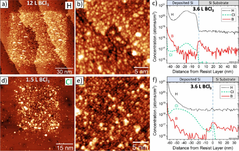
Figure 3(a) and (d) show filled-state STM images of lithographically patterned squares on H- and Cl-Si(100), respectively, after exposure to BCl3 at room temperature (20 ∘C). The H pattern in Fig. 3(a) consisted of a 80 nm 80 nm square (lithographic parameters: +7.0 V, 1.5 nA, 4 mC/cm) that was exposed to a 12 L dose of BCl3. While this dose is beyond our typical saturation dose, it provides a more robust test of the H pattern fidelity. The Cl pattern in (d) consisted of a 25 nm 25 nm square (lithographic parameters: +10.0 V, 9.0 nA, 15 mC/cm) that was exposed to a more typical 1.5 L of BCl3. The initial H- and Cl-Si(100) surfaces were first scanned with STM to verify full surface passivation. We observe that the areas outside of the patterned squares in Fig. 3(a) and (d) appear as typical H- and Cl-terminated surfaces, with the exception of some spurious dangling bonds from the depassivation process. STM images obtained away from the patterned areas after BCl3 exposure revealed that full H and Cl passivation was maintained with negligible changes in the defect concentration (see Supplemental Information). Higher magnification images of the centers of the dosed H and Cl patterns are shown in Fig. 3(b) and (e), respectively. Within the patterned area, we find a variety of features similar in appearance to those seen on the Si surface in Fig. 1(a). The clear preservation of the lithographic patterns after dosing verifies the ability of both H and Cl to mask the surface and validates their use as atomic resists for area-selective deposition of BCl3. However, the STM images do not provide a quantifiable measure of the selectivity of the adsorption on the two resist surfaces.
A more precise measure of the adsorption selectivity of BCl3 on H- and Cl-Si(100) compared to bare Si(100) was determined using SIMS. Figures 3(c) and (f) present SIMS depth profiles of B, H, and Cl from BCl3-dosed H- and Cl-Si(100) surfaces, respectively. Both fully-terminated surfaces were exposed to 3.6 L of BCl3 at room temperature (20 ∘C) and encapsulated with Si to bury the interface following the same procedure used to create the B-doped -layer samples, as discussed earlier. They were then removed from UHV and analyzed using SIMS depth profiling ex situ. The H-Si(100) sample was not heated before encapsulation with Si, while the Cl-Si(100) sample was heated to 250 ∘C for 10 minutes in an effort to drive off potential physisorbed speciesSilva-Quinones et al. (2020). However, both sample processing is still comparable as both were heated radiatively by the Si source during deposition to roughly this temperature. The depth profiles show a background B concentration in the substrate of 1017 cm-3 with buried interfaces located 45 nm and 65 nm beneath the surface of the Si capping layer on the H-Si(100) and Cl-Si(100) samples, respectively. At the buried interface, a slight increase in the B concentration above 1017 cm-3 is observed on both samples, but it is not possible to conclude from the B signal alone whether or not this increase is due to BCl3 adsorption or surface segregation of B from the substrate during sample preparationZhang et al. (1996). We have observed similar peaks in the B concentration at the Si overgrowth interface for some samples that were not exposed to BCl3 (see Supplemental Information).
However, Cl is observed in Fig. 3(c) above 1017 cm-3 within the Si capping layer indicating possible BCl3 reactions on H-Si(100). To test if the increase in B was due to a reaction with H and not adsorption at single dangling bonds present on the initial H-Si surface, a similarly prepared H-terminated Si surface was exposed to the same dose of BCl3 at 250 ∘C. SIMS of this sample revealed slightly higher concentrations of both B and Cl, indicating a thermally activated reaction, as this dosing temperature is well below the hydrogen desorption temperature (see Supplemental Information).
Cl is also observed at the interface of the Cl-Si(100) surface and in the Si capping layer at over 1018 cm-3 in Fig. 3(f). Unlike for the case of the H-Si(100) surface, it cannot be assumed that the presence this Cl is due to reactions with BCl3 as the surface was already saturated with Cl. We cannot determine quantitatively how much, if any, BCl3 reacts through the Cl resist other than it appears negligible and is several orders of magnitude lower than that seen on bare Si(100) as in Fig. 2. As Fig. 3(c) and (f) show, Cl readily migrates from the interface towards the growth surface during Si overgrowth. Even for the case of Cl-Si(100), with an initial Cl coverage approximately 1 ML, the buried interface after Si growth is left with and areal coverage of just 5.1(2) 1010 cm-2 of Cl, or ML. While the residual Cl content at the buried interface is not insignificant, i.e. it is above the background level in the substrate, the magneto-transport and device measurements presented in the following section suggests Cl does not have a detrimental impact on Hall bar measurements.
To more accurately determine the adsorption selectivity of H and Cl resists with BCl3, we compare the total areal dose of B measured by SIMS for both resists to that of bare Si(100) when all three are dosed with 3.6 L BCl3. The SIMS measurement in Fig. 2 (lower resolution B2 measurement) gives the bare Si B areal dose of 1.59(1) 1014 cm-2, while the B areal doses on the resist layers are measured from Fig. 3(c) and (f) to be 2.6(1) 1011 cm-2 for H-Si(100) and 5.2(2) 1010 cm-2 for Cl-Si(100). The adsorption selectivity ratios for these resists is then calculated in a similar manner as is done for area-selective depositionMackus et al. (2019); Gladfelter (1993):
| (1) |
where is taken to be the measured B dose in the growth area (bare Si) and is the B dose in the non-growth area (H- and Cl-terminated Si). From Eq. (1), the adsorption selectivity is found to be 310(10):1 and 1529(5):1 for H- and Cl-Si(100) at room temperature, respectively.
| Sample | BCl3 Dose | (k) | (1014 cm-2) | (cm2V-1s-1) | ||||
|---|---|---|---|---|---|---|---|---|
| B4 | 0.12 L, 20 ∘C | 7.04 | 0.395 | 21.4 | ||||
| B3 | 3.6 L, 350 ∘C | 3.69 | 1.13 | 15.0 | ||||
| B2 | 3.6 L, 20 ∘C | 1.91 | 1.90 | 38.0 |
A selectivity ratio of 1000:1 would be similar to values obtained for PH3 on H-Si(100) and, as such, is the desired goal. However, a final dopant concentration due to incorporation through the resist of 1018 cm-3 is sufficient to ensure carrier freeze out of stray adsorbed BCl3 within the resist layer at typical device measurement temperatures of 4 K. Both H and Cl resist measurements presented here result in B concentrations below that threshold, as seen in Fig. 3(c) and (f). Still, a small amount of BCl3 incorporation through the H resist could pose an issue for fabricating single-atom devices, though that remains to be determined for the amount measured here.
III.4 Electrical Characterization of B -Layers
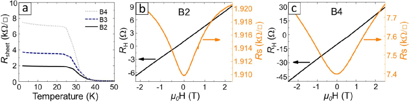
We studied the electrical transport characteristics of B-doped -layer samples B2, B3, and B4, which were fabricated into mesa-etched Hall bars 25 m 60 m in size, as described earlier. An optical micrograph of a Hall bar device is shown in the Supplemental Information. While full B incorporation was demonstrated by annealing at 500 ∘C, as shown in Fig. 1(c), -layers discussed here were not annealed that hot, as described earlier. Incorporation of dopants through annealing is typically considered important for good electrical activation, but here we wanted to isolate the effects of annealing on electrical properties and actually found that B dopant activation was high despite no deliberate incorporation. The dose parameters and measurement results of sheet resistance (), hole carrier density (), and mobility () for these samples are described in Table 1 with reported values measured at 3.0 K.
The temperature dependence of the sheet resistance between 50 K and 1.9 K is shown in Fig. 4(a) for samples B2 (solid line), B3 (dashed line), and B4 (dotted line). The measured sheet resistance values of 10 k below 30 K reflect the properties of the -layer as the resistance of the substrate and the Si capping layer increases to over 10 M at these temperatures and thus do not contribute to the measurement. Figure 4(b) and (c) show the magnetic field dependence of the longitudinal magnetoresistance, (left axis), and transverse Hall resistance, (right axis), resistance of samples B2 and B4. The positive slope of observed in (b) and (c) indicates that holes are the primary carriers in these devices, verifying that an acceptor-doped region is being measured. Likewise, the positive values of measured for these samples also indicates acceptor dopantsRamanayaka et al. (2018), as expected for a B -layer. Since APAM processes requires tight control over the entire doping and annealing process, achieving a minimum sheet resistance for sample B2 of = 1.91 k without an incorporation annealing step validates the use of BCl3 as an acceptor doping precursor. Comparing this result to -layer devices dosed with PH3 shows they are electrically similar with the sheet resistances of P-doped -layers reported to be between = 0.5 k and = 5 k for mildly dosed sampleGoh et al. (2006); Weber et al. (2012).
From the data in Fig. 4(b), the carrier density calculated for sample B2 is = 1.90 1014 cm-2 with a hole mobility = 38.0 cm2V-1s-1. This carrier density is slightly larger than the B areal dose measured by SIMS of 1.59(1) 1014 cm-2, implying full dopant activation and possibly some additional electrical pathways such as vacancies or impurities in the overgrowth layer. We compare sample B2 with B4, which was produced with a smaller BCl3 dose. The sheet resistance of B4 was larger at = 7.04 k compared to B2. The carrier density and mobility for sample B4 were both lower compared to B2 with = 3.95 1013 cm-2 and = 21.4 cm2V-1s-1. The increased carrier density of B2 is only a factor of 5 times larger than for B4 despite the BCl3 dose being a factor of 30 times larger. Suggesting that the surface of B2 may have been fully saturated by the 3.6 L dose.
Sample B3 was dosed with the same dose of BCl3 as B2 but at an elevated temperature of 350 ∘C to see if BCl3 chemisorption could be facilitated in order to increase B concentration in the -layer. As shown in Fig. 1(b), BCl3 dissociation is enhanced at this temperature relative to room temperature. However, the sheet resistance of B3 was observed to increase to = 3.69 k compared to the room temperature-dosed (20 ∘C) sample B2 as shown in Fig. 4(a), while the hole carrier density and mobility for this sample was found to decrease at = 1.13 1014 cm-2 and = 15.0 cm2V-1s-1. As with B2, a SIMS depth profile of B for B3 (not shown) measured a B areal dose similar to the carrier density of 1.17(1) 1014 cm-2. This indicates BCl3 adsorbs readily at room temperature and more so than at 350 ∘C. It is possible that at 350 ∘C, the sticking coefficient of BCl3 is decreased resulting in fewer molecules chemisorbing. Alternatively, pairs of B atoms may be starting to dimerize as they diffuse about and incorporate into the surface at this temperature, becoming electrically inactive. It has been reported in literature that P-doped -layers fabricated by dosing Si(100) with PH3 at 550 ∘C showed a similar increase in sheet resistance and decrease in carrier concentration when compared to devices dosed at room temperatureGoh et al. (2006). Comparing the SIMS depth profile measurements of the B areal doses in samples B2 and B3 indicates that the total amount of B was reduced by a factor of 0.26. This reduction does not fully explain the drop in carrier density in B3 by a factor of 0.41 compared to B2, indicating some B deactivation may also be occurring.
Sample B2 with its more optimized dosing conditions has similar properties to some P-doped -layers with reported Hall carrier densities of 2 1014 cm-2 and mobilities between = 30 cm2V-1s-1 and = 60 cm2V-1s-1Goh et al. (2006); Weber et al. (2012). Further, compared to literature values for B-doped -layer propertiesŠkereň et al. (2020) dosed with 1 L of B2H6 ( 1014 cm-2, 20 cm2V-1s-1) and 170 L of B2H6 ( 12 k) then annealed to 250 ∘C, these BCl3-dosed samples show lower values of sheet resistance with B2 also having a higher carrier density and mobility without utilizing an incorporation anneal. This result supports the notion that due to B2H6 being deposited as B dimers, many are electrically inactive without high annealing temperatures, while deposition of single B via BCl3 results in higher electrical activation.
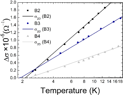
While these B-doped -layers have favorable electrical properties, their two-dimensional (2D) nature is also critical for use in APAM and quantum information applications and requires investigation. The estimated -layer width from the SIMS depth profile of Fig. 2 is not necessarily reliable evidence for a true 2D layer due to limitations of the SIMS measurement. Therefore, we use the electrical measurements to ascertain the dimensionality of the hole transport through the devices. We define a relative conductivity, , as the change in conductivity from minimum measurement temperature for each data set. This allows the data from multiple samples to be plotted together for clarity. Figure 5 shows the temperature dependence of the relative conductivity in the absence of a magnetic field with temperature plotted on a log scale for samples B2 (squares), B3 (circles), and B4 (triangles).
We then fit the data as a function of to a 2D conductance modelLee and Ramakrishnan (1985).
| (2) |
The dimensionless fitting parameter depends on the scattering mechanism of the carriers in the device and the dephasing length. The fits to the data are shown as solid lines in Fig. 5 with fit values for of = 0.84 for B2, = 0.56 for B3, and = 0.33 for B4. Similar values of have been reported for other B -layers highly doped via MBEWeir et al. (1994). Based on these fits, is found to have a linear relationship to , as seen in Fig. 5. This indicates that the transport data is consistent with 2D conductionLee and Ramakrishnan (1985), however we cannot rule out other mechanisms that contribute to a linear dependence such as electron-electron interactions based on this data alone. However, combined with the relatively thin B layer determined from the SIMS data, this analysis leads us to conclude that B-doped -layers formed from BCl3 dosing described here likely produces a 2D hole system suitable for fabrication of quantum devices in APAM applications. Obtaining a more accurate measure of the dimensionality of conduction requires further investigations such as weak localization measurement techniques, as have been done for P-doped -layersHagmann et al. (2018, 2020).
IV Conclusion
In summary, we have demonstrated the viability of BCl3 as a molecular precursor for acceptor-doping of B -layers in Si(100) for the fabrication of atomically-precise devices. B concentrations achieved in the -layers were shown to be similar to those achieved in the more well-developed processes for P-doped -layers. Importantly, BCl3 was shown to be compatible with both H- and Cl-based resists for STM lithography-based device fabrication. Cl content is not expected to be detrimental to device operation as it moves out of the buried interface towards the top of the Si epitaxial layer during growth, which can additionally be etched/polished back. Moreover, the electrical properties demonstrated here on B-doped -layers rival those of P-doping from PH3 and B-doping from B2H6 without yet optimizing the incorporation anneal step. The compatibility of BCl3 dosing with multiple resists ensures that it can be implemented in process flows including PH3 for the formation of exotic atomic-scale devices like pn junctions. The fact that BCl3 shows a slight preference for reacting with H-Si over Cl-Si could be exploited for other process applications involving halogen adsorption into patterned areas on H-Si(100)Ferng et al. (2009) to serve as a negative resist. Overall, these results point towards the suitability of BCl3 as a viable gaseous precursor for acceptor doping processes associated with atomic precision advanced manufacturing of Si-based devices.
V Acknowledgement
The authors would like to thank J. Foglebach, D. Ketchum, P. Hannah, J. Moody, S. Brown and T. Olver for their assistance with BCl3 handling and installation. We also acknowledge Matt Radue, George Wang, Ezra Bussmann, and Scott Schmucker for thought provoking discussions. This work was supported in part by the Laboratory Directed Research and Development program at Sandia National Laboratories, a multimission laboratory managed and operated by National Technology and Engineering Solutions of Sandia, LLC., a wholly owned subsidiary of Honeywell International, Inc., for the U.S. Department of Energy’s National Nuclear Security Administration under contract DE-NA-0003525. This paper describes objective technical results and analysis. Any subjective views or opinions that might be expressed in the paper do not necessarily represent the views of the U.S. Department of Energy or the United States Government.
References
- Ward et al. (2020) D. R. Ward, S. W. Schmucker, E. M. Anderson, E. Bussmann, L. Tracy, T.-M. Lu, L. N. Maurer, A. Baczewski, D. M. Campbell, M. T. Marshall, and S. Misra, (2020), arXiv:2002.11003 .
- Weber et al. (2014) B. Weber, Y. H. Tan, S. Mahapatra, T. F. Watson, H. Ryu, R. Rahman, L. C. Hollenberg, G. Klimeck, and M. Y. Simmons, Nature Nanotechnology 9, 430 (2014).
- Salfi et al. (2014) J. Salfi, M. Tong, S. Rogge, and D. Culcer, Nanotechnology 27, 244001 (2014).
- Salfi et al. (2016) J. Salfi, J. A. Mol, D. Culcer, and S. Rogge, Phys. Rev. Lett. 116, 246801 (2016).
- Shim and Tahan (2014) Y.-P. Shim and C. Tahan, Nat. Commun. 5, 4225 (2014).
- Blase et al. (2009) X. Blase, E. Bustarret, C. Chapelier, T. Klein, and C. Marcenat, Nat. Mater. 8, 375 (2009).
- Škereň et al. (2020) T. Škereň, S. A. Köster, B. Douhard, C. Fleischmann, and A. Fuhrer, Nature Electronics , 2520 (2020).
- Campbell et al. (2021) Q. Campbell, J. A. Ivie, E. Bussmann, S. W. Schmucker, A. D. Baczewski, and S. Misra, Journal of Physical Chemistry C 125, 481 (2021).
- Herner and Clark (2004) S. B. Herner and M. H. Clark, Journal of Vacuum Science & Technology B: Microelectronics and Nanometer Structures 22, 1 (2004).
- Consiglio et al. (2016) S. Consiglio, R. D. Clark, D. O’Meara, C. S. Wajda, K. Tapily, and G. J. Leusink, Journal of Vacuum Science & Technology A: Vacuum, Surfaces, and Films 34, 01A102 (2016).
- Pilli et al. (2018) A. Pilli, J. Jones, V. Lee, N. Chugh, J. Kelber, F. Pasquale, and A. LaVoie, Journal of Vacuum Science & Technology A 36, 061503 (2018).
- Duvauchelle et al. (2015) J. E. Duvauchelle, A. Francheteau, C. Marcenat, F. Chiodi, D. Débarre, K. Hasselbach, J. R. Kirtley, and F. Lefloch, Applied Physics Letters 107, 072601 (2015).
- Cammilleri et al. (2008) D. Cammilleri, F. Fossard, D. Débarre, C. T. Manh, C. Dubois, E. Bustarret, C. Marcenat, P. Achatz, D. Bouchier, and J. Boulmer, Thin Solid Films 517, 75 (2008).
- Trenhaile et al. (2006) B. R. Trenhaile, A. Agrawal, and J. H. Weaver, Appl. Phys. Lett. 89, 151917 (2006).
- Yu et al. (2008) S.-Y. Yu, H. Kim, and J.-Y. Koo, Phys. Rev. Lett. 100, 036107 (2008).
- Ferguson et al. (2009) G. A. Ferguson, U. Das, and K. Raghavachari, J. Phys. Chem. C 113, 10146 (2009).
- Deutsch et al. (1981) T. Deutsch, D. Ehrlich, D. Rathman, D. Silversmith, and R. Osgood Jr, Applied Physics Letters 39, 825 (1981).
- Kunii et al. (2004) Y. Kunii, Y. Inokuchi, A. Moriya, H. Kurokawa, and J. Murota, Applied surface science 224, 68 (2004).
- Lapiano-Smith and McFeely (1992) D. Lapiano-Smith and F. McFeely, Journal of applied physics 72, 4907 (1992).
- Ferguson et al. (2002) J. D. Ferguson, A. W. Weimer, and S. M. George, Thin Solid Films 413, 16 (2002).
- Radue et al. (2021) M. S. Radue, S. Baek, A. Farzaneh, K. J. Dwyer, Q. Campbell, A. D. Baczewski, E. Bussmann, G. T. Wang, Y. Mo, S. Misra, and R. E. Butera, (2021), arXiv:2101.09265 .
- Liu et al. (2008) Z. Liu, Z. Zhang, and X. Zhu, Physical Review B - Condensed Matter and Materials Physics 77, 035322 (2008).
- Wang and Hamers (1995) Y. Wang and R. J. Hamers, Applied Physics Letters 66, 2057 (1995).
- Gautier et al. (1996) B. Gautier, R. Prost, G. Prudon, and J. C. Dupuy, Surface and Interface Analysis 24, 733 (1996).
- Hagmann et al. (2018) J. A. Hagmann, X. Wang, P. Namboodiri, J. Wyrick, R. Murray, M. D. Stewart, R. M. Silver, and C. A. Richter, Applied Physics Letters 112, 043102 (2018).
- Weir et al. (1994) B. E. Weir, L. C. Feldman, D. Monroe, H. J. Grossmann, R. L. Headrick, and T. R. Hart, Applied Physics Letters 65, 737 (1994).
- Hagmann et al. (2020) J. A. Hagmann, X. Wang, R. Kashid, P. Namboodiri, J. Wyrick, S. W. Schmucker, M. D. Stewart, R. M. Silver, and C. A. Richter, Physical Review B 101, 245419 (2020).
- Pavlova et al. (2019) T. V. Pavlova, E. S. Skorokhodov, G. M. Zhidomirov, and K. N. Eltsov, The Journal of Physical Chemistry C 123, 19806 (2019).
- Zhang and Lagally (1994) Z. Zhang and M. G. Lagally, Physical review letters 72, 693 (1994).
- Voigtländer and Zinner (1994) B. Voigtländer and A. Zinner, Journal of Vacuum Science & Technology A: Vacuum, Surfaces, and Films 12, 1932 (1994).
- Ferng et al. (2009) S.-S. Ferng, S.-T. Wu, D.-S. Lin, and T. C. Chiang, J. Chem. Phys. 130, 164706 (2009).
- Li et al. (2011) H.-D. Li, C.-Y. Chang, L.-Y. Chien, S.-H. Chang, T.-C. Chiang, and D.-S. Lin, Phys. Rev. B 83, 075403 (2011).
- Mitsui et al. (1999) T. Mitsui, R. Curtis, and E. Ganz, J. Appl. Phys. 86, 1676 (1999).
- Dick et al. (2016) D. Dick, J. B. Ballard, R. C. Longo, J. N. Randall, K. Cho, and Y. J. Chabal, The Journal of Physical Chemistry C 120, 24213 (2016), https://doi.org/10.1021/acs.jpcc.6b08130 .
- Longo et al. (2014) R. C. Longo, S. McDonnell, D. Dick, R. M. Wallace, Y. J. Chabal, J. H. G. Owen, J. B. Ballard, J. N. Randall, and K. Cho, Journal of Vacuum Science & Technology B 32, 03D112 (2014), https://doi.org/10.1116/1.4864619 .
- Pavlova et al. (2018) T. V. Pavlova, G. M. Zhidomirov, and K. N. Eltsov, J. Phys. Chem. C 122, 1741 (2018).
- Dwyer et al. (2019) K. J. Dwyer, M. Dreyer, and R. E. Butera, J. Phys. Chem. A 123, 10793 (2019).
- Silva-Quinones et al. (2020) D. Silva-Quinones, C. He, R. E. Butera, G. T. Wang, and A. V. Teplyakov, Applied Surface Science , 146907 (2020).
- Zhang et al. (1996) Z. Zhang, M. A. Kulakov, B. Bullemer, I. Eisele, and A. V. Zotov, Applied Physics Letters 69, 494 (1996).
- Mackus et al. (2019) A. J. Mackus, M. J. Merkx, and W. M. Kessels, Chemistry of Materials 31, 2 (2019).
- Gladfelter (1993) W. L. Gladfelter, Chemistry of Materials 5, 1372 (1993).
- Ramanayaka et al. (2018) A. N. Ramanayaka, H.-S. Kim, J. A. Hagmann, R. E. Murray, K. Tang, F. Meisenkothen, H. R. Zhang, L. A. Bendersky, A. V. Davydov, N. M. Zimmerman, C. A. Richter, and J. M. Pomeroy, AIP Advances 8, 075329 (2018), https://doi.org/10.1063/1.5045338 .
- Goh et al. (2006) K. Goh, L. Oberbeck, M. Simmons, A. Hamilton, and M. Butcher, Physical Review B 73, 035401 (2006).
- Weber et al. (2012) B. Weber, S. Mahapatra, H. Ryu, S. Lee, A. Fuhrer, T. Reusch, D. Thompson, W. Lee, G. Klimeck, L. C. Hollenberg, et al., Science 335, 64 (2012).
- Lee and Ramakrishnan (1985) P. A. Lee and T. Ramakrishnan, Reviews of Modern Physics 57, 287 (1985).