Roles of the Narrow Electronic Band near the Fermi Level in 1T-TaS2-Related Layered Materials
Abstract
Here we use low-temperature scanning tunneling microscopy and spectroscopy to reveal the roles of the narrow electronic band in two 1-TaS2 related materials (bulk 1-TaS2 and 4-TaS2). 4-TaS2 is a superconducting compound with alternating 1-TaS2 and 1-TaS2 layers, where the 1-TaS2 layer has weak charge density wave (CDW) pattern and reduces the CDW coupling between the adjacent 1-TaS2 layers. In the 1-TaS2 layer of 4-TaS2, we observe a narrow electronic band located near Fermi level, and its spatial distribution is consistent with the tight-binding calculations for two-dimensional 1-TaS2 layers. The weak electronic hybridization between the 1-TaS2 and 1-TaS2 layers in 4-TaS2 shifts the narrow electronic band to be slightly above the Fermi level, which suppresses the electronic correlation induced band splitting. In contrast, in bulk 1-TaS2, there is an interlayer CDW coupling induced insulating gap. In comparison with the spatial distributions of the electronic states in bulk 1-TaS2 and 4-TaS2, the insulating gap in bulk 1-TaS2 results from the formation of a bonding band and an antibonding band due to the overlap of the narrow electronic bands in the dimerized 1-TaS2 layers.
Atomic layers with narrow electronic band near Fermi level offer unique platforms for the emergence of unconventional superconducting or magnetic phases Cao et al. (2018); Sharpe et al. (2019); Lu et al. (2019). In the narrow electronic band, the kinetic energy of the electrons is strongly reduced. When the Fermi level of the electronic system lies within the narrow band, the Coulomb interactions between electrons can significantly exceed their kinetic energy and drives the system into correlated electronic phases. When the atomic layers with narrow electronic band stack together, the interlayer coupling between the adjacent stacking layers can also strongly modify their narrow electronic bands Yankowitz et al. (2019); Ritschel et al. (2018); Wang et al. (2020). The interplay between in-plane electron-electron interactions and interlayer coupling makes the electronic properties of layered materials with narrow electronic band near Fermi level extremely complicated.
One prominent example about the important and complicated roles of the narrow electronic band near Fermi level is the origin of the low-temperature insulating phase in bulk 1-TaS2 which has been debated over the past 40 years Ritschel et al. (2018); Wang et al. (2020); Kim et al. (1994); Fazekas and Tosatti (1979); Butler et al. (2020); Ritschel et al. (2015); Lee et al. (2019). Below 350 K, the in-plane lattice distortion leads to the formation of Star-of-David (SD) cluster which consists of 13 Ta atoms Wilson et al. (1975). There is a single Ta-5d electron in each Ta site and each SD cluster has an odd number of electrons. Below 180 K, the SD clusters become long-range ordered and the bulk 1-TaS2 enters the commensurate charge density wave (CDW) state with an insulating ground state Rossnagel (2011). Without considering interlayer CDW coupling, the tight-binding simulations for two-dimensional 1-TaS2 indicate there is a very narrow electronic band near Fermi level in the commensurate CDW state of 1-TaS2 and it may be susceptible to Mott-Hubbard transition Rossnagel and Smith (2006); Smith et al. (1985). The measured low-temperature insulating gap in bulk 1-TaS2 is first interpreted as a Mott-insulating gap due to the strong electron-electron interactions [Fig. 1(a)] Kim et al. (1994); Cho et al. (2016, 2015). However, the recent scanning tunneling microscopy (STM) and angle-resolved photoemission spectroscopy (ARPES) studies demonstrate that the interlayer CDW dimerization doubles the unit cell to contain even number of Ta-5d-orbital electrons, and the insulating gap in bulk 1-TaS2 is a band insulating gap [Fig. 1(a)] Ritschel et al. (2018); Wang et al. (2020); Butler et al. (2020); Ritschel et al. (2015); Lee et al. (2019); Ma et al. (2016). In this scenario, studying the electronic properties of the 1-TaS2 layers with strongly reduced interlayer CDW coupling would be very helpful to further reveal the roles of the narrow electronic band in the 1-TaS2 layer.
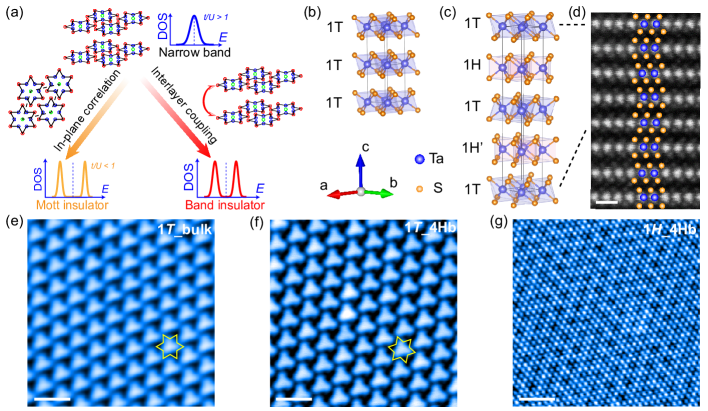
4-TaS2 is another 1-TaS2 related layered material in which the unit cell consists of alternating layers of 1-TaS2 and 1-TaS2 (half of 2-TaS2) [Fig. 1(c)]. The alternate stacking of the 1-TaS2 and 1-TaS2 layers can be clearly seen in the high-resolution transmission electron microscopy image [Fig. 1(d)]. In contrast to the low-temperature insulating phase in bulk 1-TaS2, 4-TaS2 is a superconductor with transition temperature c 3 K (see Supplemental Materials Fig.S1, Sup ). Although the CDW order exists in the 1-TaS2 layer of 4-TaS2 (1_4), the CDW order in the 1-TaS2 layer of 4-TaS2 (1_4) is very weak Ekvall et al. (1997); Han et al. (1994); Kim and Olin (1995). The 1_4 can greatly reduce the interlayer CDW coupling between adjacent 1_4, and the previous ARPES measurements indicate 1_4 and 1_4 still retain their original electronic dispersion Ribak et al. (2020). This makes 4-TaS2 an interesting platform to investigate the electronic properties of the 1-TaS2 layers with strongly reduced interlayer CDW coupling.
In this letter, we use low-temperature STM to probe and reveal the roles of the narrow electronic band in the low-temperature electronic states of 4-TaS2 and bulk 1-TaS2. We find that the narrow electronic band near Fermi level exists in the 1_4 and it is localized near the center of the SD cluster. We show that the correlation effect in the 1_4 depends on the filling factor of the narrow electronic band. We also demonstrate the relationship between the narrow electronic band in 1-TaS2 layer and the low-temperature insulating gap in bulk 1-TaS2.
Bulk 1-TaS2 and 4-TaS2 single crystals were synthesized by chemical vapor transport method with iodine as a transport agent and the detailed growth conditions were described elsewhere Gao et al. (2020); Shen et al. (2020). STM experiments were performed with a home-built low-temperature STM. Bulk 1-TaS2 and 4-TaS2 samples were cleaved at 77 K and then transferred into the low-temperature STM head for measurements at 4.3 K which is slightly above the superconducting transition temperature of 4-TaS2. Chemically etched tungsten tips were flashed by electron-beam bombardment for several minutes before use. Scanning tunneling spectroscopy (STS) measurements were done by using standard lock-in technique with 3 mV modulation at the frequency of 914 Hz.
Figure 1(e) and (f) are the negative-bias-voltage STM topographies taken on the bulk 1-TaS2 and the 1_4, respectively. The CDW pattern can be clearly seen on both these surfaces. In the negative-bias-voltage STM topography taken on the 1_4, the intrinsic CDW pattern can be barely seen [Fig. 1(g)]. Due to the CDW order in the underneath 1_4, there is a modulation pattern with the periodicity in the positive-bias-voltage STM topography taken on the 1_4 (Supplemental Materials Figs.S2 and S3, Sup ). Our STM topographies indicate that the CDW pattern in the 1_4 is weak, which makes it behaves as a buffer layer between the adjacent 1_4.
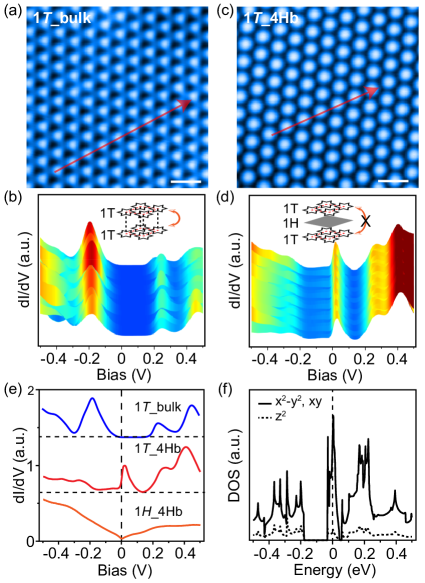
We next perform STS to study and compare the local electronic structures in bulk 1-TaS2 and 1_4. Figure 2(a) is the STM topography taken on the most typical cleave plane of bulk 1-TaS2. Figure 2(b) shows the line cut differential conductance (d/d) spectra along the red arrow shown in Fig. 2(a), where the 150 mV insulating gap induced by the interlayer dimerization effect can be clearly seen Butler et al. (2020). In comparison, Figure 2(d) shows the line cut d/d spectra taken on the 1_4 along the red arrow shown in Fig. 2(c). As shown in Fig. 2(d), there is a sharp peak feature located just above the Fermi level, and the peak width at half height is 50 mV. Another clear feature in Fig. 2d is a gap-like feature between 200mV and the Fermi level. Figure 2(e) shows the typical d/d spectra taken on the 1_4, 1_4 and the bulk 1-TaS2. The overall feature of the d/d spectrum on 1_4 is -shaped without clear electronic peaks and gaps (Supplemental Materials Figs.S4 and S5, Sup ).
Because of the 1_4, the interlayer CDW coupling between the adjacent 1_4 is reduced. To understand the features in the d/d spectrum taken on the 1_4, we compare it with the previous empirical tight-binding simulations for two-dimensional 1-TaS2 without considering the interlayer coupling [Fig. 2(f)] Rossnagel and Smith (2006). Surprisingly, the overall feature in the d/d spectrum of the 1_4 matches with the calculated density of states shown in Fig. 2(f), including the narrow band near Fermi level and the gap between 200 mV and the Fermi level. The difference is that the whole spectrum measured on the 1_4 is shifted up by 20 mV [Fig. 2(e)]. This is likely due to the weak electronic hybridization between the 1_4 and the 1_4, which induces effective doping effect to the 1_4 Shao et al. (2019). This is also consistent with the previous photoemission measurements on 4-TaS2 (Supplemental Materials Fig. S8, Sup ) Hughes and Scarfe (1995); Ribak et al. (2020).
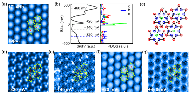
To further prove that the measured narrow electronic band near the Fermi level in the 1_4 has the same characters as the calculated narrow electronic band in the previous tight-binding simulations [Fig. 2(f)] Rossnagel and Smith (2006), we perform spatially resolved STS to map its spatial distribution and compare with the atom-projected tight-binding simulations. As shown in Fig. 3(c), there are three kinds of inequivalent Ta atoms in each SD cluster, which are labelled as ‘a’, ‘b’, and ‘c’ atoms. According to the tight-binding simulations [right panel in Fig. 3(b)] Rossnagel and Smith (2006), in the energy range of 500 mV and 500 mV, only the calculated narrow electronic band near the Fermi level has higher intensity in the central ‘a’ atom of the SD cluster. Figures 3(d)-(g) are the d/d maps taken on the same region shown in Fig. 3(a) with 320 mV, 140 mV, 20 mV, and 460 mV bias voltages, respectively. The CDW unit cell as well as the SD clusters are also outlined in each d/d map. As shown in Figs. 3(d)-(g), the narrow electronic band located near Fermi level prefers to locate in the center of the SD cluster [Fig. 3(f)] and all the other electronic bands have higher intensity at the rim of the SD cluster, which agree very well with the atom-projected density of states in the tight-binding simulations [right panel in Fig. 3(b)] Rossnagel and Smith (2006).
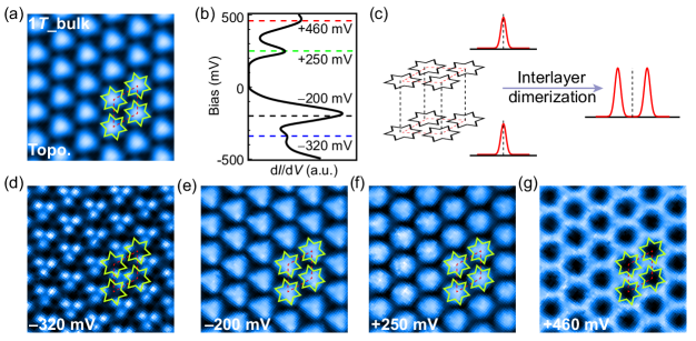
After characterizing the narrow electronic band in the 1_4, we try to explore the relationship between this narrow electronic band and the insulating gap in the bulk 1-TaS2. We also use spatially resolved STS to measure the spatial distributions of the electronic states in bulk 1-TaS2. As shown in Figs. 4(d) and (g), the spatial distributions of the electronic states at 320 mV and 460 mV are consistent with the corresponding electronic states in the 1_4 [Figs. 3(d) and (g)] which prefer to locate at the rim the SD cluster. Interestingly, the spatial distributions of the electronic peaks below and above the insulating gap [Figs. 4(e) and (f)] agree with the spatial distribution of the narrow electronic band in the 1_4 [Fig. 3(f)], which prefer to reside on the center of the SD cluster Qiao et al. (2017). The recent STM work has demonstrated that the 150 meV insulating gap in bulk 1-TaS2 [Fig. 4(b)] appears when the CDW patterns are vertical aligned in the dimerized 1-TaS2 layers [Fig. 4(c)] Butler et al. (2020). Our data further indicates that in that stacking configuration, the narrow electronic bands in the dimerized 1-TaS2 layers have strong spatial overlap and form the bonding and antibonding bands [Fig. 4(c)].
We next discuss why the narrow electronic band in the 1_4 is not splitted by the in-plane electron-electron interactions. This is likely because of the weak electronic hybridization between the 1_4 and 1_4 which shifts the narrow electronic band to be slightly above the Fermi level. This makes the narrow electronic band in the 1_4 almost unfilled, and suppresses the correlation induced electronic gap. The filling-factor-dependent correlation gap has been reported in twisted-bilayer graphene, where the correlation induced band splitting strongly depends on the filling factor of the flat electronic band Jiang et al. (2019). However, the electronic hybridization is usually sensitive to the interlayer distances between the two layers. In the 4-TaS2 sample, we find that in a few regions the narrow electronic band is located slightly closer to the Fermi level, and a 30 meV electronic gap can be detected (see Supplemental Materials Fig.9, Sup ). This 30 mV gap may be due to the electronic-correlation-induced gap in the 1_4. This also agrees with the size of the possible correlation gap (50 meV) in the undimerized 1-TaS2 layer of bulk 1-TaS2 Butler et al. (2020). For the further experiments, it would be interesting to investigate correlation effect in the 1_4 by moving the narrow electronic band closer to Fermi level with electron doping.
In summary, our data not only shows the existence of the narrow electronic band near Fermi level in 1-TaS2 layer, but also demonstrates it plays a crucial role in the low-temperature electronic properties of 1-TaS2 related materials. When the narrow electronic band in the 1_4 is located slightly above the Fermi level, the electronic correlation induced narrow band splitting is suppressed. The insulating gap in bulk 1-TaS2 originates from the interlayer CDW dimerization induced bonding and antibonding bands of the narrow electronic band. Our work also paves the way for further understanding the novel electronic phases in 1-TaS2 related materials, such as the possible chiral superconductivity in 4-TaS2 Ribak et al. (2020) and the electronic states in single layer 1-TaS2 Zhang et al. (2014); Lin et al. (2019).
S.Y. acknowledges the financial support from Science and Technology Commission of Shanghai Municipality (STCSM) (Grant No. 18QA1403100), National Science Foundation of China (Grant No. 11874042) and the start-up funding from ShanghaiTech University. J.L. acknowledges the financial support from National Science Foundation of China (Grant No. 61771234). J.J.G., X.L., W.J.L and Y.P.S. thank the support of National Key Research and Development Program under Contract No. 2016YFA0300404, the National Nature Science Foundation of China under Contracts No. 11674326 and No. 11774351, and the Joint Funds of the National Natural Science Foundation of China and the Chinese Academy of Sciences’ Large-Scale Scientific Facility under Contracts No. U1832141, No. U1932217 and U2032215. TEM experiments were supported by ShanghaiTech University and the Center for High-resolution Electron Microscopy (CEM) through EM-19430216.
References
- Cao et al. (2018) Y. Cao, V. Fatemi, S. Fang, K. Watanabe, T. Taniguchi, E. Kaxiras, and P. Jarillo-Herrero, Nature 556, 43 (2018).
- Sharpe et al. (2019) A. L. Sharpe, E. J. Fox, A. W. Barnard, J. Finney, K. Watanabe, T. Taniguchi, M. A. Kastner, and D. Goldhaber-Gordon, Science 365, 605 (2019).
- Lu et al. (2019) X. Lu, P. Stepanov, W. Yang, M. Xie, M. A. Aamir, I. Das, C. Urgell, K. Watanabe, T. Taniguchi, G. Zhang, A. Bachtold, A. H. MacDonald, and D. K. Efetov, Nature 574, 653 (2019).
- Yankowitz et al. (2019) M. Yankowitz, S. Chen, H. Polshyn, Y. Zhang, K. Watanabe, T. Taniguchi, D. Graf, A. F. Young, and C. R. Dean, Science 363, 1059 (2019).
- Ritschel et al. (2018) T. Ritschel, H. Berger, and J. Geck, Phys. Rev. B 98, 195134 (2018).
- Wang et al. (2020) Y. D. Wang, W. L. Yao, Z. M. Xin, T. T. Han, Z. G. Wang, L. Chen, C. Cai, Y. Li, and Y. Zhang, Nat. Commun. 11, 4215 (2020).
- Kim et al. (1994) J.-J. Kim, W. Yamaguchi, T. Hasegawa, and K. Kitazawa, Phys. Rev. Lett. 73, 2103 (1994).
- Fazekas and Tosatti (1979) P. Fazekas and E. Tosatti, Philos. Mag. B 39, 229 (1979).
- Butler et al. (2020) C. J. Butler, M. Yoshida, T. Hanaguri, and Y. Iwasa, Nat. Commun. 11, 2477 (2020).
- Ritschel et al. (2015) T. Ritschel, J. Trinckauf, K. Koepernik, B. Büchner, M. v. Zimmermann, H. Berger, Y. I. Joe, P. Abbamonte, and J. Geck, Nat. Phys. 11, 328 (2015).
- Lee et al. (2019) S. H. Lee, J. S. Goh, and D. Cho, Phys. Rev. Lett. 122, 106404 (2019).
- Wilson et al. (1975) J. Wilson, F. D. Salvo, and S. Mahajan, Adv. Phys. 24, 117 (1975).
- Rossnagel (2011) K. Rossnagel, J. Phys. Condens. Matter 23, 213001 (2011).
- Rossnagel and Smith (2006) K. Rossnagel and N. V. Smith, Phys. Rev. B 73, 073106 (2006).
- Smith et al. (1985) N. V. Smith, S. D. Kevan, and F. J. DiSalvo, J. Phys. C 18, 3175 (1985).
- Cho et al. (2016) D. Cho, S. Cheon, K.-S. Kim, S.-H. Lee, Y.-H. Cho, S.-W. Cheong, and H. W. Yeom, Nat. Commun. 7, 10453 (2016).
- Cho et al. (2015) D. Cho, Y.-H. Cho, S.-W. Cheong, K.-S. Kim, and H. W. Yeom, Phys. Rev. B 92, 085132 (2015).
- Ma et al. (2016) L. Ma, C. Ye, Y. Yu, X. F. Lu, X. Niu, S. Kim, D. Feng, D. Tománek, Y.-W. Son, X. H. Chen, and Y. Zhang, Nat. Commun. 7, 10956 (2016).
- (19) See Supplemental Material for detailed information on the temperature-dependent electrical resistivity of 4-TaS2, TEM image and STM topographies taken on 4-TaS2, Fourier transform images of the STM topographies taken on the 1-TaS2 layers of 4-TaS2, line cut d/d spectra on the 1-TaS2 layer of 4-TaS2, d/d maps taken on the 1-TaS2 layer of 4-TaS2, high-resolution STM topography taken on the 1-TaS2 layer of 4-TaS2, d/d maps at energies below 200 mV in the 1-TaS2 layer of 4-TaS2, comparison with the ARPES data and d/d spectra taken on the 1-TaS2 layer of 4-TaS2 showing a 30 mV gap.
- Ekvall et al. (1997) I. Ekvall, J.-J. Kim, and H. Olin, Phys. Rev. B 55, 6758 (1997).
- Han et al. (1994) W. Han, E. R. Hunt, O. Pankratov, and R. F. Frindt, Phys. Rev. B 50, 14746(R) (1994).
- Kim and Olin (1995) J.-J. Kim and H. Olin, Phys. Rev. B 52, R14388 (1995).
- Ribak et al. (2020) A. Ribak, R. M. Skiff, M. Mograbi, P. K. Rout, M. H. Fischer, J. Ruhman, K. Chashka, Y. Dagan, and A. Kanigel, Sci. Adv. 6, eaax9480 (2020).
- Gao et al. (2020) J. J. Gao, J. G. Si, X. Luo, J. Yan, Z. Z. Jiang, W. Wang, Y. Y. Han, P. Tong, W. H. Song, X. B. Zhu, Q. J. Li, W. J. Lu, and Y. P. Sun, Phys. Rev. B 102, 075138 (2020).
- Shen et al. (2020) S. Shen, B. Shao, C. Wen, X. Yuan, J. Gao, Z. Nie, X. Luo, B. Huang, Y. Sun, S. Meng, and S. Yan, Nano Lett. 20, 8854 (2020).
- Shao et al. (2019) B. Shao, A. Eich, C. Sanders, A. S. Ngankeu, M. Bianchi, P. Hofmann, A. A. Khajetoorians, and T. O. Wehling, Nat. Commun. 10, 180 (2019).
- Hughes and Scarfe (1995) H. P. Hughes and J. A. Scarfe, Phys. Rev. Lett. 74, 3069 (1995).
- Qiao et al. (2017) S. Qiao, X. Li, N. Wang, W. Ruan, C. Ye, P. Cai, Z. Hao, H. Yao, X. Chen, J. Wu, Y. Wang, and Z. Liu, Phys. Rev. X 7, 041054 (2017).
- Jiang et al. (2019) Y. Jiang, X. Lai, K. Watanabe, T. Taniguchi, K. Haule, J. Mao, and E. Y. Andrei, Nature 573, 91 (2019).
- Zhang et al. (2014) Q. Zhang, L.-Y. Gan, Y. Cheng, and U. Schwingenschlögl, Phys. Rev. B 90, 081103(R) (2014).
- Lin et al. (2019) H. Lin, W. Huang, K. Zhao, S. Qiao, Z. Liu, J. Wu, X. Chen, and S.-H. Ji, Nano Res. 13, 133 (2019).