Electric field tunable valley-Zeeman effect in bilayer graphene heterostructure: realization of the spin-orbit valve effect
Abstract
We report the discovery of electric field-induced transition from a topologically trivial to a topologically non-trivial band-structure in an atomically sharp heterostructure of bilayer graphene (BLG) and single-layer \chWSe2 per the theoretical predictions of by Gmitra et al. [Phys. Rev. Lett. 119, 146401 (2017)]. Through detailed studies of the quantum correction to the conductance in the BLG, we establish that the band-structure evolution arises from an interplay between proximity induced strong spin-orbit interaction (SOI) and the layer-polarizability in BLG. The low-energy carriers in the BLG experience an effective valley-Zeeman SOI that is completely gate-tunable to the extent that it can be switched on/off by applying a transverse displacement field or can be controllably transferred between the valence and the conduction band. We demonstrate that this results in the evolution from weak localization to weak anti-localization at a constant electronic density as the net displacement field is tuned from a positive to a negative value with a concomitant SOI-induced splitting of the low-energy bands of the BLG near the ()–valley which is a unique signature of the theoretically predicted spin-orbit valve effect. Our analysis shows that quantum correction to the Drude conductance in Dirac materials with strong induced SOI can only be explained satisfactorily by a theory that accounts for the SOI induced spin-splitting of the BLG low-energy bands. Our results demonstrate the potential for achieving highly tunable devices based on the valley-Zeeman effect in dual-gated 2-dimensional materials.
Over the last decade, the search for new quantum materials has attracted much interest from physicists and material scientists. A route to engineer new materials with desirable set of properties is via van der Waals (vdW) heterostructures of two-dimensional (2D) materials Liu et al. (2016); Geim and Grigorieva (2013); Lotsch (2015); Wang et al. (2014); Zhou et al. (2018); Novoselov et al. (2016); Kumar et al. (2018). This has led to the emergence of materials with designer properties not present in the parent components. For example, there is a particular interest in gaining the ability to manipulate the spin-degree of freedom in graphene electrically. The intrinsic SOI in graphene being very small (10eV) Gmitra et al. (2009), this endeavor has met with minimal success. Several efforts have been made to increase the SOI in graphene, including doping it with the heavy atoms Weeks et al. (2011) or topological nanoparticles Hatsuda et al. (2018); this has been achieved at the cost of degrading the quality of graphene.
Recently, both theoretical Gmitra and Fabian (2017); Khoo et al. (2017); Cummings et al. (2017); Gmitra and Fabian (2015); Offidani et al. (2017) and experimental Leutenantsmeyer et al. (2018); Island et al. (2019); Wang et al. (2016); Benítez et al. (2018); Zihlmann et al. (2018); Omar and van Wees (2018); Xu et al. (2018) studies have indicated that strong SOI can be ‘induced’ in graphene when placed on ultra-thin films of transition metal dichalcogenides (TMD). Broken inversion symmetry, coupled with the presence of heavy atoms, leads to the appearance of strong intrinsic Ising spin-orbit coupling in single-layer TMD Gmitra and Fabian (2017); Khoo et al. (2017). When placed in close proximity to graphene, the hybridization of d-orbitals of the TMD with those of carbon in graphene leads to the appearance of a large SOI in the latter. The case of BLG is particularly interesting: As the SOI is induced by a modification of the band structure of BLG, it opens up an avenue for preparing materials imbibing strong spin-polarizing SOI along with other desirable properties of BLG like high-mobility, gate-tunable bandgap, and valley/layer polarizability for possible spintronics, and optoelectronics applications Garcia et al. (2018a).
This proximity-induced SOI in the low-energy bands of BLG has two primary components – a valley-Zeeman term that causes spin-splitting of the band structure and a Kane-Mele term that opens up a topological gap at the two non-equivalent valleys, Ilić et al. (2019); Khoo et al. (2017); Gmitra and Fabian (2017); Wang et al. (2016); Garcia et al. (2018a). It was predicted that for BLG on a single-layer of \chWSe2, the strength of the SOI in the valence band (VB) of the BLG (2 meV) could be two orders of magnitude larger than that in the conduction band (CB) Gmitra and Fabian (2017). This is because the VB is formed by the non-dimer carbon atom orbitals in the BLG bottom layer, which are in proximity with \chWSe2. In contrast, the CB is formed by the non-dimer orbitals of the top layer of the BLG, where the SOI strength remains similar to that in intrinsic BLG Gmitra and Fabian (2017); Wang et al. (2015). The induced SOI is manifested as a relatively large, spin-polarized splitting of the VB of the BLG.
Further, by applying an electric field of sufficient strength perpendicular to the interface, it is possible to invert the band structure, i.e., close the bandgap and reopen it - but this time transferring the SOI induced splitting to the conduction band. Calculations show that by tuning the electric field, it is thus possible to transform the band-structure of the BLG system from a topologically trivial to non-trivial. In recent work, we have demonstrated that this leads to the appearance of the time-reversal invariant topological phase in BLG Tiwari et al. (2020). Although SOI induced splitting of the VB/CB was experimentally verified recently using penetration field capacitance measurements Island et al. (2019), direct transport observation of electric field-induced band-inversion is missing.
In this letter, we present results of magneto-transport measurements in dual gated hBN/BLG/single-layer \chWSe2/hBN heterostructures explicitly designed to explore the proposal of Gmitra et al. Gmitra and Fabian (2017). We show a precise electric field tuning of the band structure topology of BLG – from a doubly-split CB and an un-split VB at to a doubly-split VB and an un-split CB at . Thus, the band structure splitting could be controllably transferred from the VB to the CB using the electric field as an external tuning parameter. In a given band, the strength of the SOI was tunable by the electric field from a significant value to negligibly small, thus realizing the spin-orbit valve Gmitra and Fabian (2017).
We further establish out that the conventional McCann-Fal’ko (MF) equation McCann and Fal’ko (2012), which has been used almost universally to study W(A)L in graphene/TMD heterostructures, is not appropriate to quantify the weak localization physics when there is an SOI induced spin-splitting of bands, as in our case. Instead, we show that the models developed by S. Ilic et al. Ilić et al. (2019) and Ochoa et al. Ochoa et al. (2014) can account for the scattering mechanisms of the spin-split bands. We found that in the WAL case, the relevant parameters determining magneto-transport are the phase coherence time and the anti-symmetric spin relaxation (which breaks the inversion symmetry). On the other hand, in the WL regime where the induced SOI is very small, the relevant time scales are and intervalley scattering time .
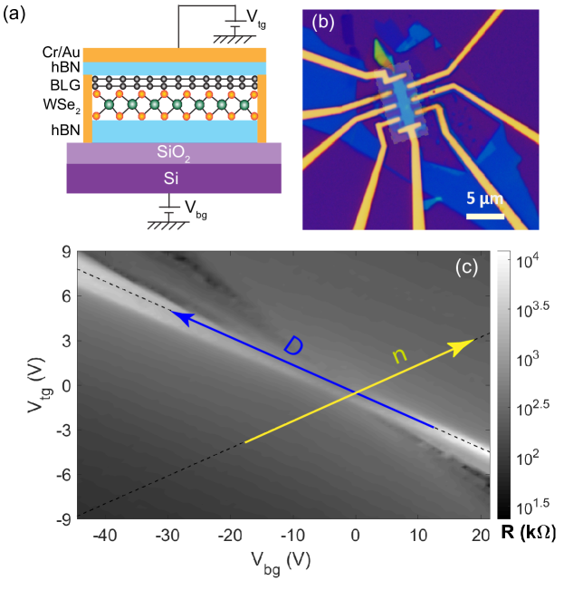
Heterostructures of hBN/BLG/single-layer \chWSe2/hBN were fabricated using standard dry transfer technique Pizzocchero et al. (2016); Wang et al. (2013) (see Supplemental Material sup ) 1). Single-layer \chWSe2 was used as it induces a much stronger SOI in BLG than thicker flakes. Fig. 1(a) is the schematic showing the dual-gated architecture of the devices. Fig. 1(b) is optical images of a device without top-gate. All electrical measurements were performed at = 20 mK in a dilution refrigerator unless specified, using standard low-frequency ac lock-in techniques.
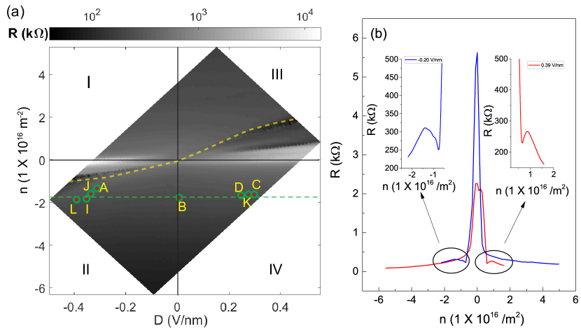
The presence of both top- and bottom-gates in the device allowed independent tuning of and via the relations and . Here, is the residual charge-density due to doping and is net internal displacement field. Fig. 1(c) shows variation of the four-probe longitudinal resistance, with and on a logarithmic scale. The blue and yellow arrows indicate the directions of increasing and , respectively. A contour plot of the logarithm of the 4-probe longitudinal resistance as functions of and ((Fig. 2(a)) shows that the resistance at the Dirac point (DP) increases with an increase in establishing the opening of a bandgap in BLG. Along with the prominent peak at DP, an asymmetric feature is observed near it as outlined by the yellow dashed curve in Fig. 2(a). This is a direct consequence of the predicted spin-splitting of the VB and CB due to proximity induced SOI in BLG Gmitra and Fabian (2017) and observed recently through penetration field capacitance studies Island et al. (2019) and transport measurements Tiwari et al. (2020).This asymmetric feature in the plane depends on the direction and magnitude of displacement field - appearing in the positive (negative) regime for positive (negative) (Fig. 2(b)).

These observations can be understood by noting that the presence of the single-layer \chWSe2 causes the BLG to experience, in addition to the strong valley-Zeeman SOI, a displacement field of the order of -0.25 V/nm making it layer-polarized. For , the Bloch waves associated with the VB and CB of the BLG reside on the bottom-layer and top-layer, respectively (Fig. 3(a)). Since the bottom layer is in close contact with the \chWSe2, the VB is prominently spin-split. This splitting increases as is made more negative via the gate-voltages. Upon changing to increasingly positive the bandgap initially closes as the external field cancels out that due to the \chWSe2. On increasing further, the bandgap reopens, but now the layer-polarization of the BLG reverses direction, causing the lower-layer to form the spin-split CB (Fig. 3(b)). Calculations show that this will cause the system to undergo a displacement field induced topological phase transition into the anomalous valley Hall phase Khoo et al. (2017) and quantum spin hall phase Tiwari et al. (2020) as recently demonstrated.
Having established displacement field induced band-inversion in our device, we move on to probe the electron dynamics as we transit from the trivial VB at to the non-trivial spin-split VB at . The SOI mechanism can be effectively probed by studying the quantum correction to the conductance in the presence of a perpendicular magnetic field . The magnetoconductance measurements were performed in the parameter space of - plane along the green line shown in Fig. 2(b) for a m-2 while changing |D| from negative to positive. To avoid contamination of the data by universal conductance fluctuation Lee and Stone (1985), each plot is an ensemble average of 40 traces measured at very close values of (spanning the range m-2).
The four-terminal magnetoconductance traces plotted in Fig. 4(a) show a clear crossover from WAL to WL as the displacement field changes from negative to positive. This transition can be understood as follows: for negative and chemical potential lying in VB (regime II in Fig. 2 and Fig. 3), the holes experience a strong SOI. This, along with the breaking of the symmetry, leads to the observed WAL McCann and Fal’ko (2012). As the displacement field becomes positive, the electrons in conduction bands experience strong SOI, while the SOI in VB reduces to a value intrinsic to BLG, which, as discussed before, is extremely small. Since the still lies in the VB (regime IV in Fig. 2 and Fig. 3), we observe WL, which is the characteristic of BLG due to its intrinsic Berry phase of 2. This transformation of the magnetoconductance from WAL to WL again demonstrates displacement field induced band-inversion in BLG/\chWSe2 heterostructures. Fig. 4(a) also shows the magnetoconductance for V/nm (blue data points). In this cross-over regime, the orbitals localized in both the upper- and the lower-layer of the BLG contribute equally to the valance and conduction bands leading to a magnetoconductance curve, which is a complex admixture of WL (arising from the intrinsic Berry curvature of unbiased BLG) and WAL (due to the induced SOC).

As mentioned earlier, the MF equation cannot be used to extract the scattering time-scales in our system, as it does not take into account the spin splitting of bands. To get a quantitative estimate of different scattering time scales involved, the magnetoconductance data was analyzed following the approach recently Ilić et al. (2019) which discusses the two different regimes taking into account the relative strengths of the SOI interaction, Zihlmann et al. (2018) and inter-valley scattering rate, . The Valley-Zeeman SOI is a strong source of symmetric spin relaxation rate Zihlmann et al. (2018); Garcia et al. (2018b). In the presence of this component of SOI, the net symmetric spin relaxation rate becomes . The asymmetric spin relaxation rate , on the other hand, arises from the Rashba SOI. When lies in VB and the CB is spin-split (), this regime is characterized by . In this WL regime, for phase coherence rate comparable to , the magnetoconductance can be analyzed using the following equation Ilić et al. (2019):
| (1) |
where , is the digamma function, and is the diffusion coefficient. For , and lying in the spin-split VB, the system is characterized by . Due to strong valley-Zeeman SOI, WL gets suppressed, and one will observe WAL described by the following equation Ilić et al. (2019):
| (2) |
where corresponds to the scattering rate . Physically corresponds to the spin-flip processes that break the symmetry induced by Rashba SOI.
Figs. 4(b,c) are plots of WL and the data were fitted using Eqn. 1. The WAL data are shown in figs. 4(d,e) and have been fitted using Eqn. 2. The extracted time-scales are tabulated in Supplemental Material sup ). In the case of WAL, was found to be ps, smaller than , which varies between 7-22 ps, consistent with the earlier observations Omar and van Wees (2018); Wang et al. (2016) and theoretical predictions Garcia et al. (2018a). For the WL case, (0.9-2 ps) was found to be smaller than (9-14 ps). The above analysis establishes that electron interference effects are dominated by spin-flip processes in the spin-split band and by inter-valley scattering in the spin-degenerate bands of BLG. It also shows that the strength of the SOI can be tuned from a significant value to negligibly small by the external electric field – this unequivocally establishes the realization of the spin-orbit valve effect and is one of the central results of this letter Gmitra and Fabian (2017).
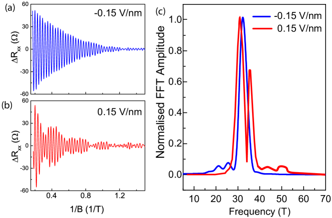
Additional support to our claim of electric field tuned band-inversion and SOI induced band-splitting comes from the results of Shubnikov-de Haas (SdH) oscillations measurements. The data were collected in a similar device of higher mobility (1,10,000 ) at a constant number density m-2. Each measurement consisted of 3000 data points and was performed for several values of between -0.15 V/nm and 0.15 V/nm. For and (regime III) we observe a beating pattern in the SdH oscillations – fig. 5(b) shows a representative data for V/nm. The beating results from the presence of two close-by frequencies of nearly equal magnitudes in the signal. The FFT data plotted in Fig. 5(c) confirms the presence of two frequencies at 31.5 T and 36.1 T reflecting the presence of two extrema of the Fermi surface at this energy. This SOI-induced band-splitting has been reported previously in BLG/\chWSe2 heterostructures Wang et al. (2016) – although in that case, a study of displacement field tunability was lacking. When the experiment was repeated for (regime I) no beating pattern was observed (see fig. 5(a) for data at V/nm) – the FFT of the data has a single peak at 32.6 T (fig. 5(c)). Thus, a clear transition from a single Fermi surface to two Fermi surfaces is observed as is varied from negative (regime I) to positive (regime III) when lies in the CB. The results of SdH oscillations complement our observation, from low-field magnetoresistance measurements, of transition from a single Fermi surface to two Fermi surfaces as is varied from positive (regime IV) to negative (regime II) for lying in the VB. We thus demonstrate ‘on-demand’ electric field induced band structure modulation of BLG over all four regimes marked in Fig. 2(a).
In summary, we demonstrate an electric field induced band structure engineering in BLG. Through magneto-transport measurements, we observe a transition from a topologically trivial to a non-trivial band in BLG. The low-energy carriers in the BLG experience an effective valley-Zeeman SOI that is gate-tunable to the extent that it can be switched on/off by applying a transverse displacement field or can be controllably transferred between the valence and the conduction band. This leads to the realization of the predicted spin-orbit valve effect.
Acknowledgements.
The authors acknowledge fruitful discussions with Tanmoy Das and Sujay Ray and facilities in CeNSE, IISc. S.K.S. acknowledges financial support from PMRF, MHRD. AB acknowledges funding from SERB (HRR/2015/000017) and DST (DST/SJF/PSA-01/2016-17).References
References
- Liu et al. (2016) Y. Liu, N. O. Weiss, X. Duan, H.-C. Cheng, Y. Huang, and X. Duan, Nature Reviews Materials 1, 16042 (2016), ISSN 2058-8437, URL https://doi.org/10.1038/natrevmats.2016.42.
- Geim and Grigorieva (2013) A. K. Geim and I. V. Grigorieva, Nature 499, 419 (2013), ISSN 1476-4687, URL https://doi.org/10.1038/nature12385.
- Lotsch (2015) B. V. Lotsch, Annual Review of Materials Research 45, 85 (2015), eprint https://doi.org/10.1146/annurev-matsci-070214-020934, URL https://doi.org/10.1146/annurev-matsci-070214-020934.
- Wang et al. (2014) H. Wang, F. Liu, W. Fu, Z. Fang, W. Zhou, and Z. Liu, Nanoscale 6, 12250 (2014), URL http://dx.doi.org/10.1039/C4NR03435J.
- Zhou et al. (2018) X. Zhou, X. Hu, J. Yu, S. Liu, Z. Shu, Q. Zhang, H. Li, Y. Ma, H. Xu, and T. Zhai, Advanced Functional Materials 28, 1706587 (2018).
- Novoselov et al. (2016) K. S. Novoselov, A. Mishchenko, A. Carvalho, and A. H. Castro Neto, Science 353 (2016), ISSN 0036-8075, URL https://science.sciencemag.org/content/353/6298/aac9439.
- Kumar et al. (2018) C. Kumar, S. K. Srivastav, P. Adhikary, S. Banerjee, T. Das, and A. Das, Physical Review B 98, 155408 (2018).
- Gmitra et al. (2009) M. Gmitra, S. Konschuh, C. Ertler, C. Ambrosch-Draxl, and J. Fabian, Physical Review B 80, 235431 (2009).
- Weeks et al. (2011) C. Weeks, J. Hu, J. Alicea, M. Franz, and R. Wu, Physical Review X 1, 021001 (2011).
- Hatsuda et al. (2018) K. Hatsuda, H. Mine, T. Nakamura, J. Li, R. Wu, S. Katsumoto, and J. Haruyama, Science advances 4, eaau6915 (2018).
- Gmitra and Fabian (2017) M. Gmitra and J. Fabian, Phys. Rev. Lett. 119, 146401 (2017), URL https://link.aps.org/doi/10.1103/PhysRevLett.119.146401.
- Khoo et al. (2017) J. Y. Khoo, A. F. Morpurgo, and L. Levitov, Nano Letters 17, 7003 (2017), pMID: 29058917, eprint https://doi.org/10.1021/acs.nanolett.7b03604, URL https://doi.org/10.1021/acs.nanolett.7b03604.
- Cummings et al. (2017) A. W. Cummings, J. H. Garcia, J. Fabian, and S. Roche, Phys. Rev. Lett. 119, 206601 (2017), URL https://link.aps.org/doi/10.1103/PhysRevLett.119.206601.
- Gmitra and Fabian (2015) M. Gmitra and J. Fabian, Phys. Rev. B 92, 155403 (2015), URL https://link.aps.org/doi/10.1103/PhysRevB.92.155403.
- Offidani et al. (2017) M. Offidani, M. Milletarì, R. Raimondi, and A. Ferreira, Phys. Rev. Lett. 119, 196801 (2017), URL https://link.aps.org/doi/10.1103/PhysRevLett.119.196801.
- Leutenantsmeyer et al. (2018) J. C. Leutenantsmeyer, J. Ingla-Aynés, J. Fabian, and B. J. van Wees, Phys. Rev. Lett. 121, 127702 (2018), URL https://link.aps.org/doi/10.1103/PhysRevLett.121.127702.
- Island et al. (2019) J. Island, X. Cui, C. Lewandowski, J. Khoo, E. Spanton, H. Zhou, D. Rhodes, J. Hone, T. Taniguchi, K. Watanabe, et al., Nature 571, 85 (2019).
- Wang et al. (2016) Z. Wang, D.-K. Ki, J. Y. Khoo, D. Mauro, H. Berger, L. S. Levitov, and A. F. Morpurgo, Phys. Rev. X 6, 041020 (2016), URL https://link.aps.org/doi/10.1103/PhysRevX.6.041020.
- Benítez et al. (2018) L. A. Benítez, J. F. Sierra, W. Savero Torres, A. Arrighi, F. Bonell, M. V. Costache, and S. O. Valenzuela, Nature Physics 14, 303 (2018), ISSN 1745-2481, URL https://doi.org/10.1038/s41567-017-0019-2.
- Zihlmann et al. (2018) S. Zihlmann, A. W. Cummings, J. H. Garcia, M. Kedves, K. Watanabe, T. Taniguchi, C. Schönenberger, and P. Makk, Phys. Rev. B 97, 075434 (2018), URL https://link.aps.org/doi/10.1103/PhysRevB.97.075434.
- Omar and van Wees (2018) S. Omar and B. J. van Wees, Phys. Rev. B 97, 045414 (2018), URL https://link.aps.org/doi/10.1103/PhysRevB.97.045414.
- Xu et al. (2018) J. Xu, T. Zhu, Y. K. Luo, Y.-M. Lu, and R. K. Kawakami, Phys. Rev. Lett. 121, 127703 (2018), URL https://link.aps.org/doi/10.1103/PhysRevLett.121.127703.
- Garcia et al. (2018a) J. H. Garcia, M. Vila, A. W. Cummings, and S. Roche, Chem. Soc. Rev. 47, 3359 (2018a), URL http://dx.doi.org/10.1039/C7CS00864C.
- Ilić et al. (2019) S. Ilić, J. S. Meyer, and M. Houzet, Phys. Rev. B 99, 205407 (2019), URL https://link.aps.org/doi/10.1103/PhysRevB.99.205407.
- Wang et al. (2015) Z. Wang, D.-K. Ki, H. Chen, H. Berger, A. H. MacDonald, and A. F. Morpurgo, Nature Communications 6, 8339 (2015), ISSN 2041-1723, URL https://doi.org/10.1038/ncomms9339.
- Tiwari et al. (2020) P. Tiwari, S. K. Srivastav, S. Ray, T. Das, and A. Bid, ACS nano (2020).
- McCann and Fal’ko (2012) E. McCann and V. I. Fal’ko, Phys. Rev. Lett. 108, 166606 (2012), URL https://link.aps.org/doi/10.1103/PhysRevLett.108.166606.
- Ochoa et al. (2014) H. Ochoa, F. Finocchiaro, F. Guinea, and V. I. Fal’ko, Phys. Rev. B 90, 235429 (2014), URL https://link.aps.org/doi/10.1103/PhysRevB.90.235429.
- Pizzocchero et al. (2016) F. Pizzocchero, L. Gammelgaard, B. S. Jessen, J. M. Caridad, L. Wang, J. Hone, P. Bøggild, and T. J. Booth, Nature communications 7, 1 (2016).
- Wang et al. (2013) L. Wang, I. Meric, P. Huang, Q. Gao, Y. Gao, H. Tran, T. Taniguchi, K. Watanabe, L. Campos, D. Muller, et al., Science 342, 614 (2013).
- (31) See Supplemental Material at [URL will be inserted by APS] for addition raw data and detailed discussion on device fabrication, measurement techniques and analysis which includes Refs.Gorbachev et al. (2007) (????).
- McCann and Koshino (2013) E. McCann and M. Koshino, Reports on Progress in Physics 76, 056503 (2013), URL https://doi.org/10.1088%2F0034-4885%2F76%2F5%2F056503.
- Lee and Stone (1985) P. A. Lee and A. D. Stone, Physical review letters 55, 1622 (1985).
- Garcia et al. (2018b) J. H. Garcia, M. Vila, A. W. Cummings, and S. Roche, Chemical Society Reviews 47, 3359 (2018b).
- Gorbachev et al. (2007) R. Gorbachev, F. Tikhonenko, A. Mayorov, D. Horsell, and A. Savchenko, Physical review letters 98, 176805 (2007).
See pages - of Supplementary.pdf