Robust wavefront dislocations of Friedel oscillations in gapped graphene
Abstract
Friedel oscillation is a well-known wave phenomenon, which represents the oscillatory response of electron waves to imperfection. By utilizing the pseudospin-momentum locking in gapless graphene, two recent experiments demonstrate the measurement of the topological Berry phase by corresponding to the unique number of wavefront dislocations in Friedel oscillations. Here, we study the Friedel oscillations in gapped graphene, in which the pseudospin-momentum locking is broken. Unusually, the wavefront dislocations do occur as that in gapless graphene, which expects the immediate verification in the current experimental condition. The number of wavefront dislocations is ascribed to the invariant pseudospin winding number in gaped and gapless graphene. This study deepens the understanding of correspondence between topological quantity and wavefront dislocations in Friedel oscillations, and implies the possibility to observe the wavefront dislocations of Friedel oscillations in intrinsic gapped two-dimensional materials, e.g., transition metal dichalcogenides.
Since the seminal discovery of grapheneNovoselov et al. (2004), two-dimensional materials have attracted wide interest because of their novel physics and great potential applicationsLiu et al. (2020). Usually, two-dimensional materials have high mobility, in which the antiparticles move ballistically and exhibit unconventional quantum tunneling and interferenceKatsnelson et al. (2006); Young and Kim (2009); Cheianov et al. (2007); Beenakker et al. (2009); Wu et al. (2011); Castro Neto et al. (2009). One can intentionally add one or two impurities to form the impurity-design system, this kind of system is charming because it is easily handled theoretically and experimentally, and then it can be regarded as the model system for the exploration of ballistic physicsSettnes et al. (2014a). Experimentally, scanning tunneling spectroscopy (STM) is a proper tool for impurity-design systemBasov et al. (2014). More interesting, the dimension of two-dimensional materials are very unique. On one hand, the bare surface properties of two-dimensional materials are also the bulk properties in contrast to three-dimensional materials. On the other hand, different from the one-dimensional materials, two-dimension materials with two-dimensional parameter space is enough to evolve the global topological quantityDutreix et al. (2020). Therefore, surface-sensitive STM measurement is promising to explore the topological physics of impurity-design two-dimensional materials.
Friedel oscillations (FO) is the quantum interference of electronic waves scattering by the imperfection in crystalline host materialsFriedel (1952). Recently, STM has been demonstrated experimentally to measure the topological Berry phase of monolayer graphene by counting wavefront dislocations in Friedel oscillations, which is induced by the intentional hydrogen adatom Dutreix et al. (2019). One subsequent experiment shows that for bilayer graphene FOs can exhibit , , or wavefront dislocations explained by the Berry phase, the specific sublattice positions of the single impurity and the position of STM tipZhang et al. (2020). Electronic Berry phase as the intrinsic nature of the wave functions is defined in momentum space, which is responsible for many exotic electronic dynamics such as the index shift of quantum Hall effect in monolayer grapheneNovoselov et al. (2005); Zhang et al. (2005) and bilayer grapheneNovoselov et al. (2006), Klein tunnelingKatsnelson et al. (2006); Young and Kim (2009) and the weak antilocalization Wu et al. (2007). The probe of Berry phase usually requires the magnetic fieldXiao et al. (2010); Novoselov et al. (2005); Zhang et al. (2005); Young and Kim (2009). These two experiments not only do not need external magnetic field, but also realize the measurement of Berry phase in real space. However, two experiments both focus on the gapless cases for graphene and emphasize the relation between Berry phase and wavefront dislocation number. This attracts us to explore the effect of gap opening on the interference pattern of FOs.
Gap opening in graphene occurs in various different ways with the substrate coupling as a typical exampleChaves et al. (2020). Most experiments and devices are performed on the substrate-supported graphene, in which lattice mismatch induced inversion symmetry breaking makes Berry phase unquantized multiple of Yao et al. (2008). As a result, gap opening should challenge the established correspondence relation between Berry phase and wavefront dislocation number in previous experimentsDutreix et al. (2019); Zhang et al. (2020). In this study, we study the FOs in gapped graphene. Comparing to the gapless graphene, gapped graphene does not have pseudospin-momentum locking, this may prohibit the occurrence of characteristic interference structure (namely, wavefront dislocations) in FOs following the intuitive picture as suggested by the seminal work Dutreix et al. (2019). But the wavefront dislocations in FOs do emerge. Here, we explain the origin of wavefront dislocations by the invariant pseudospin winding number in gaped and gapless graphene, which can be regarded as an updated correspondence relation compatible with the previous experimentsDutreix et al. (2019); Zhang et al. (2020). The wavefront dislocations in FOs of gapped graphene can be verified in the present experimental conditions, and this study helps deepen the understanding of topological physics reflected in the FOs of the impurity-design system.
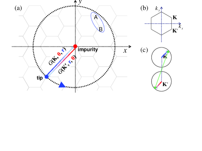
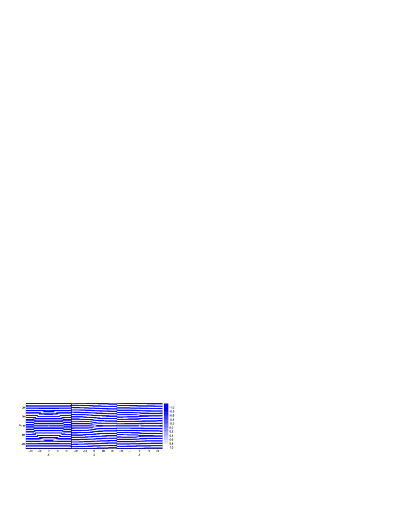
Fig. 1 gives the schematic measurement of impurity-induced electronic density oscillation of monolayer graphene by STM. The present experimental technology allows one to intentionally introduce a single-atom vacancy on arbitrary sublattice site of grapheneGonzalez-Herrero et al. (2016), e.g., on the sublattice as shown by the red dot in Fig. 1(a). Corresponding to the introduction of the single vacancy, FOs occur, and lead to the change of the space-resolved and energy-resolved local density of states (LDOS) Bena (2008); Zou et al. (2016):
| (1) |
where represents the change of the total Green’s function (GF) or propagator incorporating the effect of the vacancy relevant to the bare propagator of host system (i.e., graphene in Fig. 1(a)), and has the form
| (2) |
Here, the -matrix approach is used to describe the effect of vacancy whose potential is simulated by , and -matrix isDutreix and Katsnelson (2016)
| (3) |
In the -matrix, is usually a matrix and its form depends on the specific position of the vacancy, e.g., in Fig. 1(a) (for the other vacancy configuration in supplementary materials), it is
| (4) |
For graphene, there are two Dirac valleys in the Brillouin zoneCastro Neto et al. (2009) (cf. Fig. 1(b)), and , then are contributed by the intravalley and intervalley scattering. In graphene, the intravalley scattering contribution to has been well understood through many theoreticalCheianov and Falko (2006); Bena (2008); Hwang and Das Sarma (2008); Pereg-Barnea and MacDonald (2008); Bena (2009); Pellegrino et al. (2009); Bacsi and Virosztek (2010); Gomez-Santos and Stauber (2011); Lawlor et al. (2013); Settnes et al. (2014b); Settnes et al. (2015); Dutreix and Katsnelson (2016); Rusin and Zawadzki (2018) and experimentalRutter et al. (2007); Brihuega et al. (2008); Mallet et al. (2012); Clark et al. (2014); Gonzalez-Herrero et al. (2016) efforts, while intervalley scattering contribution attracts people’s attention very recently due to its underlying topological natureDutreix et al. (2019); Zhang et al. (2020); Zhang and He (2020). is measured easily by STM. FOs of are dominated by the backscattering events along the constant energy contourSprunger et al. (1997); Zhang et al. (2019). Focusing on the intervalley scattering, the corresponding physical process of Eq. 2 is shown in Fig. 1(a), i.e., STM tip emits the electron waves from one valley , as shown by the propagator , scattering by the vacancy back to STM tip through the other valley , as shown by the propagator . Of course, the conjugate process also exists, i.e., the emission/scattering waves are from valley. Here, is the matrix element of matrix and is associated with the valley momentum index. When the STM tip is shifted around the vacancy in real space as shown in Fig. 1(a), the contributing momentum states to the propagator change their momentum around and as shown in Fig. 1(c). As a result, the Berry phase defined in momentum space is measured by STM in real space, and the key is the pseudospin-momentum lockingDutreix et al. (2019). In contrast, we will show that the pseudospin winding number instead of Berry phase is measured by STM in gaped graphene without pseudospin-momentum locking.
The physics is essentially the same for gapped monolayer and bilayer graphene, described below using gapped monolayer as an example and the relevant results for gapped bilayer graphene in supplementary materials. The Hamiltonian of gaped monolayer graphene is . is expressed in the sublattice basis of , then is the Pauli matrix acting on the pseudospin space. is the staggered potential on the sublattice and , which originates from the inversion symmetry breaking, e.g., by the proximity substrateZhou et al. (2007); Chaves et al. (2020). And is valley index for two inequivalent valleys in graphene, with being the carbon-carbon bond length and being the nearest-neighbor hopping energy, and / is used as the length/enegy unit in our conventionCastro Neto et al. (2009). The energy spectrum and the spinor wavefunction are, respectively,
| (5) |
and
| (6) |
where the reduced quantities are defined as , with for the conduction and the valence band. The GF in momentum space is defined as , and it is
| (7) |
Here, with for the retarded properties of GF and the Fermi level is assumed in the conduction band for brevity. Performing the Fourier transformation to the momentum space GF, we express the real space GFZhu et al. (2011) as with
| (8) |
where is -th order Handel function of the first kind, , , and ( is the module (azimuthal angle) of . Concentrating on the intervalley contribution, the change of LDOS is
| (9) |
where the sublattice-resolved LDOS are
| (10a) | ||||
| (10b) | ||||
| Here, , , and is the matrix element of -matrix induced by the vacancy on the sublattice . | ||||
Nontrivially, Eq. 2 for the LDOS contributed by the intervalley scattering has the identical form as that in gapless graphene Dutreix et al. (2019) and it reproduces the result of gapless case when . For the vacancy on the sublattice , is trivial. for the intervalley scattering, then the phase of is singular at . By shifting STM tip around the vacancy, i.e., is rotated by , there should be additional wavefronts in the Friedel oscillation pattern of Dutreix et al. (2019). In Fig. 2, focusing on the intervalley scattering contribution, we show electronic density oscillations around a single-atom vacancy and on sublattice (left panel) and on sublattice (middle panel), respectively. And the sum as total electronic density modulation (right panel). As expected, exhibit the normal oscillating wavefronts perpendicular to with a wavelength , and does not display any topological feature. gives two wavefront dislocations at , which accommodates for the phase accumulated along the contour enclosing the singular point of the phase Nye et al. (1974). In the total electronic density modulation (cf. right panel of Fig. 2), only shifts the position of dislocations from along the direction parallel to , but does not change the shape and the number of dislocationsDutreix et al. (2019).
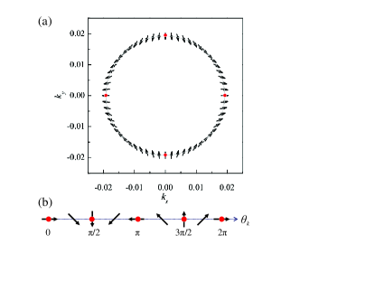
The number of additional wavefronts is regarded as the signature of the Berry phase of graphene. However, the correspondence between Berry phase and the wavefront dislocation number fails since the Berry phase is unquantized multiple of in gapped graphene. Back to Fig. 1(c), in which we do not follow the referencesDutreix et al. (2019); Zhang et al. (2020) to plot the momentum-resolved pseudospin direction, but it still shows synchronous motion of the dominant scattering state contributing to FOs in momentum space and STM tip in real space, e.g., the scattering state rotates clockwise/counterclockwise on the constant energy contour when STM tip is shifted clockwise/counterclockwise around the vacancy. The scattering state can be used to define the pseudospin vector where
| (11a) | ||||
| (11b) | ||||
| Due to and , Eq. 11 gives fixing points with the momentum azimuthal angle , , , and , at which the pseudospin directions are fixed. This feature has no dependence on , then is robust to the gap opening. To show more visually, we arbitrarily choose a set of parameters to plot the pseudospin texture in Fig. 3. With the scattering state moving on the constant energy contour, the pseudospin direction twists continuously in Fig. 3(a). Clearly, there are fixing points shown by the red dots (cf. Fig. 3(a)), which implies the invariant pseudospin winding number. Referring to Fig. 3(b), when evolves from to , the pseudospin rotates by corresponding to the winding number . Alternatively, the invariant pseudospin winding number can also be shown mathematicallyFuchs et al. (2010). To rewrite the gapped Hamiltonian of monolayer graphene into the form: | ||||
| (12) |
where the azimuthal and polar angles on the Bloch sphere are defined as , with and Arg. As a result, we obtain the Berry phase along a closed Fermi surface:
| (13) |
Here, we have used the Berry connection . Most importantly, the winding number is introduced
| (14) |
While the Berry phase of Eq. 13 has the dependence and becomes unquantized multiple of , of Eq. 14 with the absolute value is topologically invariant in gapless and gapped graphene. As a result, the wavefront dislocations also exist in gapped graphene, which should be ascribed to the invariant winding number.
Here, we firstly discuss the experimental implication of our theoretical discovery. When for gapless graphene, one can say that the Berry phase and winding number are equivalent, then Berry phase is measured by the wavefront dislocationsDutreix et al. (2019); Zhang et al. (2020). But a supplementary experiment is necessary to confirm the gapless nature of graphene sample. In previous two experimentsDutreix et al. (2019); Zhang et al. (2020), there is no such supplementary experiment and they do not perform the quantitative comparison between experiments and simulations for the FOs, which both prohibit the discovery of the possible gap opening. The quantitative calculations of FOs, especially properly incorporating the strength and range of impurity potential, is rather important and is worth of further simulations, e.g., by using density functional calculationsNoori et al. (2020). Also, this experimental discussions are also applicable to one recent theoretical proposal, which uses the presence or absence of wavefront dislocations in FOs to distinguish the incompatible low-energy models for twisted bilayer graphenePhong and Mele (2020). In light of present experimental technology, we expect the immediate verification of our theoretical prediction in gapped graphene. In addition, our results may stimulate the theoretical and experimental research interest on the FOs in intrinsic gapped two-dimensional materials, e.g., transition metal dichalcogenidesWang et al. (2012); Schaibley et al. (2016).
The robustness of the wavefront dislocations of FOs to the gap opening dictates the potential applications in graphene-based pseudospintronicsPesin and MacDonald (2012). Each imperfection can be regarded as one vortex, and the sublattice dependence of wavefront dislocation help define the vortex and antivortex since the orientations of the tripod shape of the imperfection on two sublattices are differentDutreix et al. (2019). Then, we can use the vortex/antivortex as 0/1 to construct the memory device. And the the writing of vortex-based memory device can be performed by using STM to shift the imperfection from one sublattice to the other oneGonzalez-Herrero et al. (2016), while its reading is realized by scanning the imperfection-induced FOs to characterize the orientations of the tripod shape of the imperfection. One recent experimentZhang and He (2020) studies the effect of spacing on the wavefront dislocation of two vortices, and shows the irrelevant vortices on the several nanometer scale which favors the high-density of vortex-based memory device. This implies the great potential of impurity-design graphene in pseudospintronics.
In summary, we have studied the Friedel oscillation in gapped graphene. Although the pseudospin-momentum locking is broken, the wavefront dislocations still emerge in intervalley scattering contributed Friedel oscillations. We establish the correspondence between the invariant winding number instead of the Berry phase and the number of wavefront dislocations in gapped graphene, which can be verified by the present experimental technology. This study is helpful to the understanding of correspondence between topological quantity and wavefront dislocations in Friedel oscillations, and broadens the range of materials to observe the wavefront dislocations of FOs, e,g, in transition metal dichalcogenidesWang et al. (2012); Schaibley et al. (2016).
Acknowledgements
The authors thank Dr. Li-Kun Shi for helpful discussions. This work was supported by the National Key RD Program of China (Grant No. 2017YFA0303400), the National Natural Science Foundation of China (NSFC) (Grants No. 11774021 and No. 11504018), and the NSAF grant in NSFC (Grant No. U1930402). We acknowledge the computational support from the Beijing Computational Science Research Center (CSRC).
References
- Novoselov et al. (2004) K. S. Novoselov, A. K. Geim, S. V. Morozov, D. Jiang, Y. Zhang, S. V. Dubonos, I. V. Grigorieva, and A. A. Firsov, Science 306, 666 (2004).
- Liu et al. (2020) C. Liu, H. Chen, S. Wang, Q. Liu, Y.-G. Jiang, D. W. Zhang, M. Liu, and P. Zhou, Nature Nanotechnology 15, 545 (2020).
- Katsnelson et al. (2006) M. I. Katsnelson, K. S. Novoselov, and A. K. Geim, Nat. Phys. 2, 620 (2006).
- Young and Kim (2009) A. F. Young and P. Kim, Nat. Phys. 5, 222 (2009).
- Cheianov et al. (2007) V. V. Cheianov, V. Fal’ko, and B. L. Altshuler, Science 315, 1252 (2007).
- Beenakker et al. (2009) C. W. J. Beenakker, R. A. Sepkhanov, A. R. Akhmerov, and J. Tworzydło, Phys. Rev. Lett. 102, 146804 (2009).
- Wu et al. (2011) Z. Wu, F. Zhai, F. M. Peeters, H. Q. Xu, and K. Chang, Phys. Rev. Lett. 106, 176802 (2011).
- Castro Neto et al. (2009) A. H. Castro Neto, F. Guinea, N. M. R. Peres, K. S. Novoselov, and A. K. Geim, Rev. Mod. Phys. 81, 109 (2009).
- Settnes et al. (2014a) M. Settnes, S. R. Power, D. H. Petersen, and A.-P. Jauho, Phys. Rev. Lett. 112, 096801 (2014a).
- Basov et al. (2014) D. N. Basov, M. M. Fogler, A. Lanzara, F. Wang, and Y. Zhang, Rev. Mod. Phys. 86, 959 (2014).
- Dutreix et al. (2020) C. Dutreix, M. Bellec, P. Delplace, and F. Mortessagne, Wavefront dislocations reveal insulator topology (2020), eprint 2006.08556.
- Friedel (1952) J. Friedel, The London, Edinburgh, and Dublin Philosophical Magazine and Journal of Science 43, 153 (1952).
- Dutreix et al. (2019) C. Dutreix, H. Gonzlez-Herrero, I. Brihuega, M. I. Katsnelson, C. Chapelier, and V. T. Renard, Nature 574, 219 (2019).
- Zhang et al. (2020) Y. Zhang, Y. Su, and L. He, Phys. Rev. Lett. 125, 116804 (2020).
- Novoselov et al. (2005) K. S. Novoselov, A. K. Geim, S. V. Morozov, D. Jiang, M. I. Katsnelson, I. V. Grigorieva, S. V. Dubonos, and A. A. Firsov, Nature 438, 197 (2005).
- Zhang et al. (2005) Y. Zhang, Y.-W. Tan, H. L. Stormer, and P. Kim, Nature 438, 201 (2005).
- Novoselov et al. (2006) K. S. Novoselov, E. McCann, S. V. Morozov, V. I. Falko, M. I. Katsnelson, U. Zeitler, D. Jiang, F. Schedin, and A. K. Geim, Nature Physics 2, 177 (2006).
- Wu et al. (2007) X. Wu, X. Li, Z. Song, C. Berger, and W. A. de Heer, Phys. Rev. Lett. 98, 136801 (2007).
- Xiao et al. (2010) D. Xiao, M.-C. Chang, and Q. Niu, Rev. Mod. Phys. 82, 1959 (2010).
- Chaves et al. (2020) A. Chaves, J. G. Azadani, H. Alsalman, D. R. daCosta, R. Frisenda, A. J. Chaves, S. H. Song, Y. D. Kim, D. He, J. Zhou, et al., npj 2D Materials and Applications 4, 29 (2020).
- Yao et al. (2008) W. Yao, D. Xiao, and Q. Niu, Phys. Rev. B 77, 235406 (2008).
- Gonzalez-Herrero et al. (2016) Gonzalez-Herrero, Hector, Brihuega, Ivan, Ugeda, Miguel, M., Gomez-Rodriguez, Jose, and M. and, Science 352, 437 (2016).
- Bena (2008) C. Bena, Phys. Rev. Lett. 100, 076601 (2008).
- Zou et al. (2016) Y.-L. Zou, J. Song, C. Bai, and K. Chang, Phys. Rev. B 94, 035431 (2016).
- Dutreix and Katsnelson (2016) C. Dutreix and M. I. Katsnelson, Phys. Rev. B 93, 035413 (2016).
- Cheianov and Falko (2006) V. V. Cheianov and V. I. Falko, Phys. Rev. Lett. 97, 226801 (2006).
- Hwang and Das Sarma (2008) E. H. Hwang and S. Das Sarma, Phys. Rev. Lett. 101, 156802 (2008).
- Pereg-Barnea and MacDonald (2008) T. Pereg-Barnea and A. H. MacDonald, Phys. Rev. B 78, 014201 (2008).
- Bena (2009) C. Bena, Phys. Rev. B 79, 125427 (2009).
- Pellegrino et al. (2009) F. M. D. Pellegrino, G. G. N. Angilella, and R. Pucci, Phys. Rev. B 80, 094203 (2009).
- Bacsi and Virosztek (2010) A. Bcsi and A. Virosztek, Phys. Rev. B 82, 193405 (2010).
- Gomez-Santos and Stauber (2011) G. Gomez-Santos and T. Stauber, Phys. Rev. Lett. 106, 045504 (2011).
- Lawlor et al. (2013) J. A. Lawlor, S. R. Power, and M. S. Ferreira, Phys. Rev. B 88, 205416 (2013).
- Settnes et al. (2014b) M. Settnes, S. R. Power, D. H. Petersen, and A.-P. Jauho, Phys. Rev. B 90, 035440 (2014b).
- Settnes et al. (2015) M. Settnes, S. R. Power, J. Lin, D. H. Petersen, and A.-P. Jauho, Phys. Rev. B 91, 125408 (2015).
- Rusin and Zawadzki (2018) T. M. Rusin and W. Zawadzki, Phys. Rev. B 97, 205410 (2018).
- Rutter et al. (2007) Rutter, M. G., J. N. Crain, Guisinger, P. N., T., N. First, P., Stroscio, and A. J., Science 317, 219 (2007).
- Brihuega et al. (2008) I. Brihuega, P. Mallet, C. Bena, S. Bose, C. Michaelis, L. Vitali, F. Varchon, L. Magaud, K. Kern, and J. Y. Veuillen, Phys. Rev. Lett. 101, 206802 (2008).
- Mallet et al. (2012) P. Mallet, I. Brihuega, S. Bose, M. M. Ugeda, J. M. Gomez-Rodriguez, K. Kern, and J. Y. Veuillen, Phys. Rev. B 86, 045444 (2012).
- Clark et al. (2014) K. W. Clark, X.-G. Zhang, G. Gu, J. Park, G. He, R. M. Feenstra, and A.-P. Li, Phys. Rev. X 4, 011021 (2014).
- Zhang and He (2020) Y. Zhang and L. He, arXiv (2020), eprint 2008.03956.
- Sprunger et al. (1997) P. T. Sprunger, L. Petersen, E. W. Plummer, E. Laegsgaard, and F. Besenbacher, Science 275, 1764 (1997).
- Zhang et al. (2019) S.-H. Zhang, D.-F. Shao, and W. Yang, Journal of Magnetism and Magnetic Materials 491, 165631 (2019).
- Zhou et al. (2007) S. Y. Zhou, G.-H. Gweon, A. V. Fedorov, P. N. First, W. A. deHeer, D.-H. Lee, F. Guinea, A. H. Castro Neto, and A. Lanzara, Nature Materials 6, 770 (2007).
- Zhu et al. (2011) J.-J. Zhu, D.-X. Yao, S.-C. Zhang, and K. Chang, Phys. Rev. Lett. 106, 097201 (2011).
- Nye et al. (1974) J. F. Nye, M. V. Berry, and F. C. Frank, Proceedings of the Royal Society of London. A. Mathematical and Physical Sciences 336, 165 (1974).
- Fuchs et al. (2010) J. N. Fuchs, F. Piechon, M. O. Goerbig, and G. Montambaux, The European Physical Journal B 77, 351 (2010).
- Noori et al. (2020) K. Noori, S. Y. Quek, and A. Rodin, Phys. Rev. B 102, 195416 (2020).
- Phong and Mele (2020) V. O. T. Phong and E. J. Mele, Phys. Rev. Lett. 125, 176404 (2020).
- Wang et al. (2012) Q. H. Wang, K. Kalantar-Zadeh, A. Kis, J. N. Coleman, and M. S. Strano, Nature Nanotechnology 7, 699 (2012).
- Schaibley et al. (2016) J. R. Schaibley, H. Yu, G. Clark, P. Rivera, J. S. Ross, K. L. Seyler, W. Yao, and X. Xu, Nature Reviews Materials 1, 16055 (2016).
- Pesin and MacDonald (2012) D. Pesin and A. H. MacDonald, Nat. Mater. 11, 409 (2012).