Distinguishing a Mott Insulator from a Trivial Insulator with Atomic Adsorbates
Abstract
In an electronic system with various interactions intertwined, revealing the origin of its many-body ground state is challenging and a direct experimental way to verify the correlated nature of an insulator has been lacking. Here we demonstrate a way to unambiguously distinguish a paradigmatic correlated insulator, a Mott insulator, from a trivial band insulator based on their distinct chemical behavior for a surface adsorbate using 1T-TaS2, which has been debated between a spin-frustrated Mott insulator or a spin-singlet trivial insulator. We start from the observation of different sizes of spectral gaps on different surface terminations and show that potassium adatoms on these two surface layers behave in totally different ways. This can be straightforwardly understood from distinct properties of a Mott and a band insulators due to the fundamental difference of a half and a full-filled orbital involved respectively. This work not only solves an outstanding problem in this particularly interesting material but also provides a simple touchstone to identify the correlated ground state of electrons experimentally.
Introduction.—When a material has strong interactions in various degrees of freedom, such as charge, spin, orbital, lattice, disorder, and topology, our understanding of the system’s ground state and phase evolution is largely limited, and intriguing quantum phenomena emerge. The competition of a few different interactions often makes it truly challenging to identify the origin of the material’s ground state, such as the high-temperature superconductivity Keimer2015 , which would be crucial to control its macroscopic properties and functionalize the material. For a simple but paradigmatic example, the Mott insulating state is driven by strong on-site Coulomb interaction of electrons () for a material with a half-filled electron band, which would otherwise form a metallic state Mott1968 . This state is usually distinguished by the existence of an energy gap in spectroscopy against the theoretical prediction of a gapless state without the inclusion of Mott1968 . However, there has been no direct experimental way to verify the half-filled insulating state and distinguish it from a band insulator with a full-filled electron band. The situation becomes more complicated when there exist competing insulating states of different origins, such as the charge or spin density wave states. In this Letter, we introduce a simple but powerful method to straightforwardly distinguish a Mott insulator from a band insulator based on the chemical difference in a half and a full-filled electronic orbital.
As a critical example to show the limitation in distinguishing a Mott insulator under various different interactions, we take a layered transition metal dichalcogenide 1T-TaS2. This material has been assumed widely as a Mott insulator with a coexisting charge-density-wave state Fazekas1979 ; Giambattista1990 ; Kim1994 ; Kim1996 ; Zwick1998 ; Pillo2000 ; Rossnagel2005 ; Sipos2008 ; Xu2010 ; Ang2012 ; Ang2013 ; Stojchevska2014 ; Lahoud2014 ; Ang2015 ; Cho2015 ; Cho2016 ; Law2017 ; Cho2017 ; Ribak2017 ; Ligges2018 ; Lutsyk2018 ; Skolimowski2019 ; Park2019 ; Cheng2020 but there exist a few other degrees of freedom to be considered. It undergoes a characteristic series of phase transitions from a metal to a commensurate charge-density-wave (CCDW) phase through a nearly commensurate charge-density-wave (NCCDW) phases Wilson1975 . A common unit cell of CDW phases has 13 Ta atoms distorted into a David-star(DS)-shape cluster to form a superstructure Wilson1975 . 13 5 electrons of a unit cell, one from each Ta atom, form 6 full-filled and one half-filled band with its electron localized strongly on the central Ta atom. The system exhibits a metal-insulator transition accompanying the NCCDW-CCDW transition and the strong localization of the half-filled electron, a very small bandwidth to amplify , provides a natural ground of a Mott insulator model Fazekas1979 . The model prevailed the scene for more than three decades Fazekas1979 ; Giambattista1990 ; Kim1994 ; Kim1996 ; Zwick1998 ; Pillo2000 ; Rossnagel2005 ; Sipos2008 ; Xu2010 ; Ang2012 ; Ang2013 ; Stojchevska2014 ; Lahoud2014 ; Ang2015 ; Cho2015 ; Cho2016 ; Law2017 ; Cho2017 ; Ribak2017 ; Ligges2018 ; Lutsyk2018 ; Skolimowski2019 ; Park2019 ; Cheng2020 and fueled the recent proposal of a quantum spin liquid state to explain the absence of a magnetic ordering down to a very low temperature Law2017 ; Ribak2017 .
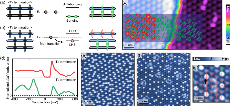
However, the Mott insulator model is seriously challenged by a few recent band structure calculations Ritschel2015 ; Ritschel2018 ; Lee2019 . Very importantly, the above model ignores the interlayer hopping of electrons, which can crucially affect the bandwidth. The experiments seem to favor a bilayer stacking order, the layers within the bilayer stacked without a lateral translation Ishiguro1991 ; Witte2019 ; Stahl2020 ; Butler2020 ; Wang2020 [a TA stacking, Fig. 1(a)] and each bilayer unit stacked with a translation of a half unit cell Witte2019 ; Butler2020 [a TC stacking, Fig. 1(b)], where half-filled Ta 5 electrons within bilayers form a spin-singlet state to lead to a trivial bonding-antibonding energy gap against the Mott insulator model. In our point of view, while tracking the intriguing interlayer ordering is very important, this situation manifests the weakness of the current method to verify a Mott insulating state, which relies crucially on the band structure calculation.
Methods.—1T-TaS2 single crystal was cleaved in high vacuum and K atoms were deposited in a ultra high vacuum at room temperature. STM images were obtained at 4.4 K by a constant-current mode with a sample bias of -600 (TC) or -800 meV (TA) depending on the terminations suppl . A lock-in technique with a modulation of 1 kHz was utilized for measurements. After the measurements on the adsorption behavior, K adatoms were removed by through mild electric field applied by an STM tip in order to determine the layer stacking suppl .
First-principles calculations were performed using the projected augmented plane-wave method implemented in the Vienna ab initio simulation package Blochl1994 ; Kresse1996 and the generalized gradient approximation for the exchange and correlation potential Perdew1996 . Spin-orbit coupling was also included. Electronic wave functions were expanded in plane waves with an energy cutoff of 400 eV. The isolated and K-adsorbed TaS2 layers were considered within supercell geometries where the interlayer spacing was 20 Å. Geometries were relaxed until the forces on each atom were less than 0.01 eV Å-1. We used a 771 and 331 k-point grid to sample the entire Brillouin zone for the pristine and K-adsorbed 1T-TaS2 system, respectively.
Different surface terminations with distinct adsorption behavior.—The bilayer stacking would manifest itself as the existence of two distinct, inter- and intra-bilayer, terminations (TA and TC terminations, respectively) on the cleaved surface [Figs. 1(a) and 1(b)]. Indeed, a very recent STM experiment observed both terminations but with different sizes of the band gap Butler2020 . However, the nature of each band gap is unclear. We pick up two neighboring surface layers separated by a single-layer-height step [Figs. 1(c) and 1(d)] and assign accurately the centers of DS clusters through the numerical processing of the STM images and compared them quantitatively between the neighboring layer. The top layer corresponds to the TC termination, which inevitably requests the bottom one as TA based on the alternative TA-TC stacking order at low temperature Witte2019 ; Butler2020 . They both exhibit insulating tunneling spectra [the normalized differential tunneling conductance ()] but with different band gaps of 250 and 400 meV as shown in Fig. 1(d), which is quantitatively consistent with the recent STM results Butler2020 ; suppl .
These two terminations are sharply contrasted by a simple electron-donating adsorbate of K as illustrated in the STM images of Figs. 1(e)-1(g). The most apparent is that the adsorption behaviors of K atoms are distinct on different terminations. On the TC termination [Fig. 1(e)], all K atoms sit on the center of a DS cluster as reported recently Lee2020 , and the surface unit cells bifurcate into two groups, DS with and without K adatom at their center. On the other hand, we observe two different adsorbate configurations on the TA termination. The bright ones are at the center of the DS clusters as on the TC termination, but there exist off-centered adsorbates [medium contrast protrusions in Figs. 1(f) and 1(g)] mostly between neighboring DS clusters. The off-centered adsorbates are metastable configurations, which are prone to hop and easily perturbed by STM tips. The distinct adsorption behavior of the neighboring terraces is uniformly observed over different areas surfaces and in different cleavages.
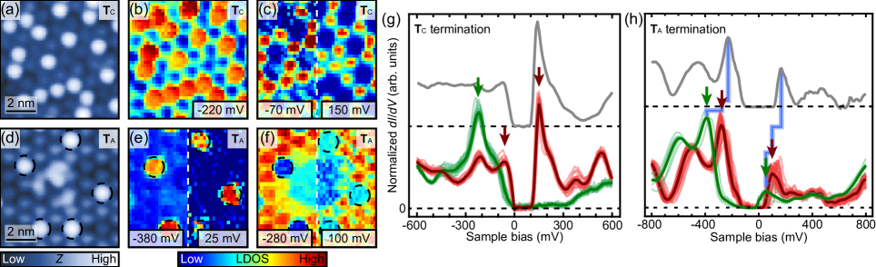
Distinct electronic states of different surface terminations with adsorbates.—The difference between two different terminations becomes more evident in the spectroscopic measurements. The DS clusters with central K adsorbates exhibit strong local density of states (LDOS) at different energies, -220 meV on the TC [Figs. 2(a) and 2(b)], and 25 and -380 meV on the TA termination [Figs. 2(d) and 2(e)] as shown in the LDOS maps. The corresponding spectra reveal more important details. The DS clusters without K on the TC termination show no change of the LDOS while those with K have a single strong LDOS peak at -220 meV replacing the two peaks defining the energy gap at the Fermi level [Fig. 2(g)] suppl . This is natural for a Mott insulator since the half-filled electron in a unit cell with a K adsorbate would be fully saturated by the electron from the adsorbate. Since the full-filled electron orbital is strongly localized, the neighboring bare unit cells would have little doping effect [Figs. 2(c) and 2(g)]. In stark contrast, on the TA termination, the two LDOS peaks defining the band gap are rigidly shifted to lower energies for the DS clusters without an adsorbate and to even lower energy for those with K [Fig. 2(h)] suppl . This straightforwardly indicates that the K adsorbates dope the system. The rigid shift upon doping is what is expected in a band insulator. The doping effect is stronger on the DS cluster with K adsorbate and weaker on those without [see their LDOS maps in Figs. 2(e) and 2(f)].
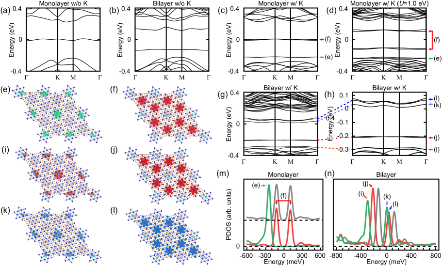
DFT calculations with a single and a bilayer model.—All experimental results are well explained by the DFT calculations with an isolated single and a bilayer layer model for the TC and TA termination, respectively. The validity of the single-layer model can be confirmed by a trilayer model suppl and is easily understood from a marginal overlap of half-filled electrons between the top and the second layer. Even before any calculation, the difference of the electronic system is obvious. In contrast to the single layer with half-filled electrons, there exist an even number of electrons in a double-layer unit cell, which would form an interlayer bonding on each unit cell to fall into a simple band insulator [Fig. 1(a)]. These result in totally different single-particle band structures, a metallic band at the Fermi level [Fig. 3(a)] and insulating bonding-antibonding bands [Fig. 3(b)] in a single and a double layer, respectively. As well known, introducing electron correlation in the single layer would open a Mott gap but does not affect substantially the bonding-antibonding bands suppl .
The K adsorption on both terminations is modeled with a periodic occupation of 1/3 of DS clusters, which results in a superstructure. As detailed previously, on the TC termination, this superstructure is highly favored due to the dipole-dipole interaction of adsorbates Lee2020 . When K atoms are deposited, its 4 electron forms a strong local bonding with electron at the center of the DS [Fig. 3(e)] and a full-filled band at -200 meV [Fig. 3(c)]. The electrons in the bare DS clusters are almost intact [Fig. 3(f)] with their partially-filled band remaining at the Fermi level [Fig. 3(c)] or Mott Hubbard bands [Fig. 3(d)] when is excluded or included, respectively. The corresponding partial density of states [PDOS, Fig. 3(m)] reproduce well the spectroscopic data suppl , two distinct spectra on a K-adsorbed and a bare DS cluster, as mentioned above [Fig. 2(g)]. On the TA termination, in clear contrast, the 4 electron is donated to the bands to shift them rigidly. There exist different amounts of shifts for the DS clusters with and without K adsorbates, a larger shift for the former, as observed in the experiment, giving rise to basically two sets of bands with wave functions on different unit cells [Figs. 3(g), 3(h), and 3(i)-3(l)]. The inclusion of does not affect the overall band structure but only increases the band gap marginally (15 meV) suppl . The PDOS changes [Fig. 3(n)] match excellently with the experimental data [Fig. 2(h)] suppl .
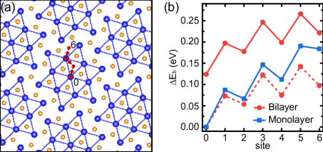
Details of the adsorption behavior.—As we mentioned above, the difference of the surface termination appears not only in spectroscopy but also in the adsorbate distribution as the existence of the minor adsorption sites on the TA termination. This can also be explained within the DFT calculations. In principle, there are 28 symmetrically inequivalent adsorption sites in a DS cluster Lee2020 . We first exclude those on top of surface sulfur atoms, which are energetically unfavored. The adsorption energy is found to be minimized at the DS center but depends on the termination as -2.85 and -2.73 eV on TC and TA termination, respectively. A larger adsorption energy gain is expected on the TC termination due to the localized half-filled electrons as discussed above. As shown for 7 representative sites [Fig. 4(a)] with different distances from the center, the adsorption energy increases rather linearly with the distance from the center [Fig. 4(b)]. We note the relatively large difference of the adsorption energy between the site 5 and 6 on the TA than the TC termination. Note also that the energy difference between the site 6 and the most stable site (site 0) is much large on the TC termination. Thus, the adatom migration to a more stable sites toward the center of a DS cluster is much easier on the TC termination. These adsorption-energy landscapes qualitatively explain the absence/presence of adsorbates on the site 6 in the experiment on the TC/TA termination suppl . While the difference in the adsorbate distribution is easily observable in the topographic imaging, its origin is not as fundamental as the spectroscopic difference on different terminations. However, roughly speaking, the origin of the difference can be traced back to the stronger bonding of the electron-donating adsorbate on the Mott insulator due to the half-filled electron. Combining all the experimental and theoretical result consistently, we introduce that the adsorption of monovalent adsorbates can be a direct and unique touchstone to distinguish a Mott insulator from a band insulator or other types of insulators based on filled orbitals.
This work was supported by the Institute for Basic Science (Gradnt No. IBS-R014-D1). K.-H. Jin is supported by the Institute for Basic Science (Grant No. IBS-R014-Y1).
References
- [1] B. Keimer, S. A. Kivelson, M. R. Norman, S. Uchida, and J. Zaanen, From quantum matter to high-temperature superconductivity in copper oxides, Nature 518, 179 (2015).
- [2] N. F. Mott, Metal-Insulator Transition, Rev. Mod. Phys. 40, 677 (1968).
- [3] P. Fazekas and E. Tosatti, Electrical, structural and magnetic properties of pure and doped , Philos. Mag. B 39, 229 (1979).
- [4] B. Giambattista, C. G. Slough, W. W. McNairy, and R. V. Coleman, Scanning tunneling microscopy of atoms and charge-density waves in , , and , Phys. Rev. B 41, 10082 (1990).
- [5] J.-J. Kim, W. Yamaguchi, T. Hasegawa, and K. Kitazawa, Observation of Mott Localization Gap Using Low Temperature Scanning Tunneling Spectroscopy in Commensurate , Phys. Rev. Lett. 73, 2103 (1994).
- [6] J.-J. Kim, I. Ekvall, and H. Olin, Temperature-dependent scanning tunneling spectroscopy of , Phys. Rev. B 54, 2244 (1996).
- [7] F. F.Zwick et al., Spectral Consequences of Broken Phase Coherence in , Phys. Rev. Lett. 81, 1058 (1998).
- [8] T. Pillo et al., Interplay between electron-electron interaction and electron-phonon coupling near the Fermi surface of , Phys. Rev. B 62, 4277 (2000).
- [9] K. Rossnagel, E. Rotenberg, H. Koh, N. V. Smith, and L. Kipp, Continuous Tuning of Electronic Correlations by Alkali Adsorption on Layered , Phys. Rev. Lett. 95, 126403 (2005).
- [10] B. Sipos et al., From Mott state to superconductivity in , Nat. Mater. 7, 960 (2008).
- [11] P. Xu et al., Superconducting phase in the layered dichalcogenide upon inhibition of the metal-insulator transition, Phys. Rev. B 81, 172503 (2010).
- [12] R. Ang et al., Real-Space Coexistence of the Melted Mott State and Superconductivity in Fe-Substituted , Phys. Rev. Lett. 109, 176403 (2012).
- [13] R. Ang et al., Superconductivity and bandwidth-controlled Mott metal-insulator transition in 1-TaS2-xSex, Phys. Rev. B 88, 115145 (2013).
- [14] L. Stojchevska et al., Ultrafast Switching to a Stable Hidden Quantum State in an Electronic Crystal, Science 344, 177 (2014).
- [15] E. Lahoud, O. N. Meetei, K. B. Chaska, A. Kanigel, and N. Trivedi, Emergence of a Novel Pseudogap Metallic State in a Disordered 2D Mott Insulator, Phys. Rev. Lett. 112, 206402 (2014).
- [16] R. Ang et al., Atomistic origin of an ordered superstructure induced superconductivity in layered chalcogenides, Nat. Commun. 6, 6091 (2015).
- [17] D. Cho, Y.-H. Cho, S.-W. Cheong, K.-S. Kim, and H. W. Yeom, Interplay of electron-electron and electron-phonon interactions in the low-temperature phase of , Phys. Rev. B 92, 085132 (2015).
- [18] D. Cho et al., Nanoscale manipulation of the Mott insulating state coupled to charge order in , Nat. Commun. 7, 10453 (2016).
- [19] K. T. Law and P. A. Lee, as a quantum spin liquid, Proc. Natl. Acad. Sci. 114, 6996 (2017).
- [20] D. Cho et al., Correlated electronic states at domain walls of a Mott-charge-density-wave insulator , Nat. Commun. 8, 392 (2017).
- [21] A. Ribak et al., Gapless excitations in the ground state of , Phys. Rev. B 96, 195131 (2017).
- [22] M. Ligges et al., Ultrafast Doublon Dynamics in Photoexcited -, Phys. Rev. Lett. 120, 166401 (2018).
- [23] I. Lutsky et al., Electronic structure of commensurate, nearly commensurate, and incommensurate phases of by angle-resolved photoelectron spectroscopy, scanning tunneling spectroscopy, and density functional theory, Phys. Rev. B 98, 195425 (2018).
- [24] J. Skolimowski, Y. Gerasimenko, and R. Žitko, Mottness collapse without metallization in the domain wall of the triangular-lattice Mott insulator , Phys. Rev. Lett. 122, 036802 (2019).
- [25] J. W. Park, G. Y. Cho, J. Lee, and H. W. Yeom, Emergent honeycomb network of topological excitations in correlated charge density wave, Nat. Commun. 10, 4038 (2019).
- [26] L. Cheng et al., Renormalization of the Mott gap by lattice entropy: The case of 1T-, Phys. Rev. Res. 2, 023064 (2020).
- [27] J. A. Wilson, F. J. Di Salvo, and S. Mahajan, Charge-density waves and superlattices in the metallic layered transition metal dichalcogenides, Adv. Phys. 24, 117 (1975).
- [28] T. Ritschel et al., Orbital textures and charge density waves in transition metal dichalcogenides, Nat. Phys. 11, 328 (2015).
- [29] T. Ritschel, H. Berger, and J. Geck, Stacking-driven gap formation in layered 1T-, Phys. Rev. B 98, 195134 (2018).
- [30] S.-H. Lee, J. S. Goh, and D. Cho, Origin of the Insulating Phase and First-Order Metal-Insulator Transition in , Phys. Rev. Lett. 122, 106404 (2019).
- [31] Y. D. Wang et al., Band insulator to Mott insulator transition in 1T-TaS2, Nat. Commun. 11, 4215 (2020).
- [32] C. J. Butler, M. Yoshida, T. Hanaguri, and Y. Iwasa, Mottness versus unit-cell doubling as the driver of the insulating state in , Nat. Commun. 11, 2477 (2020).
- [33] T. Ishiguro and H. Sato, Electron microscopy of phase transformations in 1T-, Phys. Rev. B 44, 2046 (1991).
- [34] G. von Witte et al., Surface structure and stacking of the commensurate charge density wave phase of , Phys. Rev. B 100, 155407 (2019).
- [35] W. Stahl et al., Collapse of layer dimerization in the photo-induced hidden state of 1T-TaS2, Nat. Commun. 11, 1247 (2020).
- [36] See the Supplemental Material at [URL will be given by the publisher] for the details, which includes Refs. Cho2016 ; Ma2016 ; Wang2020 ; Butler2020 .
- [37] P. E. Blöchl, Projector augmented-wave method, Phys. Rev. B 50, 17953 (1994).
- [38] G. Kresse, and J. Furthmüller, Efficient iterative schemes for ab initio total-energy calculations using a plane-wave basis set, Phys. Rev. B 54, 11169 (1996).
- [39] J. P. Perdew, K. Burke, and M. Ernzerhof, Generalized Gradient Approximation Made Simple, Phys. Rev. Lett. 77, 3865 (1996).
- [40] J. Lee et al., Honeycomb-Lattice Mott Insulator on Tantalum Disulphide, Phys. Rev. Lett. 125, 096403 (2020).
- [41] L. Ma et al., A metallic mosaic phase and the origin of Mott-insulating state in 1T-TaS2, Nat. Commun. 7, 10956 (2016).