[orcid=0000-0002-8157-3534] \cormark[1] \creditConceptualization, Software & Investigation, synthesis & characterization, Writing
[orcid=0000-0003-3719-8535] \creditConceptualization, Software Investigation
[orcid=0000-0002-1775-6598] \creditInvestigation, Writing - review editing
[orcid=0000-0002-8572-1485] \creditInvestigation and Supervision
[orcid=0000-0003-0418-5375] \creditConceptualization, Funding acquisition, Investigation, Supervision, Writing - review editing
[orcid=0000-0003-2168-853X] \fnmark[1] \creditConceptualization, Funding acquisition, Investigation, Methodology, Supervision, Writing - review editing
[cor1]Corresponding author \fntext[fn1]On sabatical leave at ICF-UNAM from CIICAP-UAEM
Optimization of wide-band quasi-omnidirectional 1-D photonic structures
Abstract
We have designed, optimized, fabricated and characterized highly reflective quasi-omnidirectional (angular range of ) multilayered structures with a wide spectral range. Two techniques, chirping (a continuous change in thicknesses) and stacking of Bragg-type sub-structures, have been used to enhance the reflectance with minimum thickness for a given pair of refractive indices. Numerical calculations were carried out employing the transfer matrix method and we optimized the design parameters to obtain maximal reflectance averaged over different spectral ranges for all angles. We fabricated some of the optimized structures with porous silicon dielectric multilayers with low refractive contrast and compared their measured optical properties with the calculations. Two chirped structures with thicknesses 21.6 m and 60.4 m, resulting in quasi omnidirectional mirrors with bandwidths of 360 nm and 1800 nm, centered at 1160 nm and 1925 nm respectively have been shown. In addition, we fabricated a stacked sub-Bragg mirror structure with a quasi omnidirectional bandwidth of 1800 nm (centered at 1850 nm) and a thickness of 41.5 m, which is almost two third (in thickness) of the chirped structure. Thus, our techniques allowed us to obtain relatively thin quasi-omnidirectional mirrors with wide bands over different wavelength ranges. Our analysis techniques can be used for the optimization of the reflectance not only in multilayered PS systems with different refractive index contrasts but also for systems with other types of materials with low refractive index contrast. The present study could also be useful for obtaining omnidirectional dielectric mirrors in large spectral regions using different materials, flat focusing reflectors, thermal regulators, or, if defects are included, as filters or remote chemical/biosensors with a wide angular independent response.
keywords:
Optimized reflectance \sepOmnidirectional structures \sepChirped structures \sepStacked Bragg mirror structures1 Introduction
Photonic crystal (PC)-based structures have been extensively investigated due to their light controlling properties [1, 2]. Photons entering a PC interact with its periodically varying dielectric constant and their energies are consequently organized into photonic bands. In analogy to electronic bands withiny a crystal, propagation is forbidden if the energy lies within certain regions known as photonic band gaps (PBG’s). Thus, the PC behaves as a mirror if illuminated by light with frequencies within in a PBG. For several applications it is useful to fabricate ommnidirectional mirrors with an absolute band gap for all angles of incidence. The use of metallic mirrors is limited due to their relatively large absorption at the visible (Vis) and near infrared (NIR) frequencies. An attractive alternative consists of low-absorption dielectric structures, which may be designed for specific frequency ranges. One-dimensional (1D) and two-dimensional (2D) PCs have applications in optoelectronics, optical telecommunications and computing, laser technology [3, 4], and radiative cooling applications [5]. The simplest 1D-PC is composed of a finite number of periodically alternating layers of high and low refractive indices, with corresponding thicknesses and chosen so that their optical thicknesses corresponds to a quarter of a wavelength at a nominal wavelength . This yields a Bragg mirror (BM) which might have a large PBG including an omnidirectional gap if the contrast and the number of periods are large enough. Mirrors with high reflectance within a wider frequency range may be engineered by using different nominal wavelengths for different layers. One way to obtain such structures is to gradually change the width of the layers as a function of their depth, producing chirped-type structures [6]. Another alternative is to stack BMs, in such a way that their reflection bands partially overlap each other at their edges, resulting in a wider high-reflection band [7].
On the other hand, different fabrication techniques have been used to obtain omnidirectional mirrors (ODM) that operate on the visible and/or near infrared (Vis-NIR) range of the electromagnetic spectrum. For example, Chen et al. [8], reported the fabrication of a structure made of six pairs of TiO2/SiO2 layers with an omnidirectional band (ODB) of about 70 nm in the NIR range, employing a sol-gel deposition method. Park et al. [9], used molecular beam epitaxy to grow a stack of four pairs of GaAs/AlAs layers, followed by its conversion to GaAs/Al2O3 by selective oxidation of the AlAs layers, to obtain an ODB from 710 to 950 nm. On the other hand, DeCorby et al. [10], fabricated mirrors by coupling multiple layers of Ge33As12Se55 chalcogenide glass and polyamide-imide deposited by thermal evaporation and spin-casting respectively, to obtain a 150 nm wide omnidirectional band centered at 1750 nm. Furthermore, Jena et al. [11], used sequential asymmetric bipolar pulsed DC magnetron sputtering for TiO2 layers and radio frequency magnetron sputtering for SiO2 layers to generate TiO2/SiO2 1D-PC’s and achieved an ODB from 592 to 668 nm. However, these techniques are expensive and they require sophisticated equipment and long fabrication times. Use of porous silicon (PS) is an attractive alternative, since it can be easily manufactured by electrochemical etching crystalline Si in an hydrofluoric acid based electrolyte to obtain a sponge-like nanostructure composed of Si and air. By modulating the supplied current and its application time during the electrochemical reaction, it is possible to obtain multilayered structures allowing for the fabrication ODM’s [12, 13]. Although optical filters [14, 15] are the most common application of PS PC’s, they have also been widely used as chemical sensors [16, 17], waveguides [18] and for photoluminescence control [19]. Recently, the study of chirped multilayer structures has increased due to their possible application as flat focusing mirrors [20, 21, 22]. PS based dielectric optical filters, quasi-ODM’s and ODM’s have been extensively studied in different regions of the electromagnetic spectrum, such as the ultraviolet (UV) [23], visible [24], and NIR [25] regions. However, to obtain the desirable high index of refraction contrast, layers of high porosity have to be employed, which makes the resulting structures relatively fragile. In addition, use of high porosity makes the fabrication of large structures, with a very large number of layers, unfeasible. For this reason, in this work we study different strategies to produce multilayered mirrors with high reflectance omnidirectional band with relatively small thickness and refractive index contrast.
This paper is organized as follows. In Sec. 2 we develop the methods used to design and calculate the reflectance spectra of the PS multilayered structures such as chirped structures and mirror stacks. In Sec. 3 we provide details about the fabrication of these structures. In Sec. 4 we present the numerical and experimental results corresponding to our proposed structures and compare them to previous reports. We obtained significantly large band-widths with relatively thinner structures than reported previously. Finally, we discuss our conclusions in Section 5.
2 Theory
For the analysis of the propagation of electromagnetic fields through multilayered systems it is usual to employ the transfer matrix method [26, 27]. Assuming the system is 1D, with variations only along the directions, and that the polarization of light is either transverse electric (TE) or transverse magnetic (TM), the transfer matrix is a 2x2 matrix that relates the components of the electric and magnetic fields parallel to the plane evaluated at to their value at ,
Many equivalent formulations have been proposed to obtain and use [28, 29, 30]. Here we use a recently developed formalism for the numerically stable calculation of the reflectance of large multilayer systems, as proposed by Puente-Díaz, et al. [31], summarized in the supplementary information. The explicit expressions for the optical coefficients are:
| (1) |
and
| (2) |
where are the elements of the transfer matrix which transfer the fields from its surface interface with vacuum at towards the substrate at , is the surface impedance of vacuum and is the surface impedance of the substrate, and we define and in terms of the reflected and transmitted fields, where we choose the ’s as electric fields for (TE) polarization and magnetic fields for transverse magnetic polarization (TM). Here, and for TE polarization, while and for TM polarization. The reflectance is given by and the transmittance by with for TE polarization and for TM polarization. The complex refractive index of the porous layers were obtained through the Bruggeman’s effective medium theory, which has been reported to adequately reproduce the optical parameters of PS [16, 32, 33].
3 Experimental details
Some of the proposed photonic structures were synthesized through anodic etching of a (100) oriented, -type Boron doped, crystalline Si wafer with resistivity 0.002-0.005 cm, under galvanostatic conditions [34, 35]. The electrochemical anodization process was performed at room temperature, with an electrolyte of aqueous hydrofluoric acid (HF) (48 of wt) and ethanol (99.9 of wt) in 1:1 volumetric proportion, respectively. However, as it is not desirable to use very high porosity contrasts due to structure fragility and electrolyte diffusivity problems [36], the current densities were chosen as 35 and 305 , with corresponding porosities of 51% and 76%, respectively. These porosities were determined through previously obtained calibration curves using a gravimetric technique [32]. The etching rate of PS was obtained by synthetizing single layers under similar conditions and measuring their thicknesses through Scanning Electron Microscopy (SEM). Absolute reflectivity measurements were carried out with a Perkin Elmer Lambda 950 UV/Visible spectrophotometer with a variable angle universal reflectance accessory (URA) for different incident angles , , , , and using non-polarized light. The maximum and minimum values of were constrained by the angular range of the URA.
4 Results and discussion
In this section we present optimized calculations of the reflectance of different multilayered omnidirectional wide-band mirrors and we compare the results with experimental spectra taken from the corresponding samples at diferent angles of incidence. Sec. 4.1 is devoted to chirped-type Bragg mirrors while Sec. 4.2 is devoted to structures made of stacked sub-mirrors.
We develop two techniques to design multilayer photonic structures. In the first, the wavelength () to which the -th pair of layers is tuned is determined by a given function of . Several functions are proposed and their parameters are optimized to maximize the reflectance averaged over a given spectral and angular range. The second technique consisted in stacking sub-mirrors tuned to different wavelengths, chosen so that their spectral ranges overlap. For each sub-mirror, the spectral range was obtained from the dispersion relation of a corresponding periodic structure. The degree of overlap was optimized to maximize . The optimizations were done employing the Minuit module [37] of the Perl Data Language (PDL) [38].
4.1 Chirped-type Bragg mirrors
Here we study multilayered structures where the thicknesses for each pair of layers are tuned to a wavelength which changes gradually with the depth of the layer, according to
| (3) |
where and are the minimum and maximum design wavelengths respectively, is the number of periods in the structure, and is a smooth function that goes from 0 to 1 as its argument goes from the surface () to the substrate (. We only consider increasing functions due to the high absorption of PS in the ultraviolet region, which decreases in the visible and becomes negligible in the near infrared, so, that the first periods are tuned in the UV-Vis regions. We consider the following classes of functions:
| (4) |
| (5) |
and
| (6) |
where , and are parameters to optimize in order to maximize the average reflectance over given spectral and angular ranges. The class (Eq. (4)) with corresponds to simple increasing profiles, is the arithmetic mean of two functions of the type with different powers and , and (Eq. (6)) is designed so that the first term dominates near the surface and the second near the substrate, to allow different behaviors at the edges of the spectrum. The parameters , , and were optimized to maximize the reflectance for non-polarized light averaged in the angular range of to and either in the spectral region from 350 to 1400 nm or from 400 to 3000 nm. For we took as another parameter to be optimized while was fixed at 1400 nm. For we fixed both nm and nm. In the first case, we decided to optimize to obtain the best design in the high absorption zone of the PS. Approximately of the solar radiation that reaches the earth’s surface is contained in the spectral region , and in [39]. A direct application of the optimized structures in these regions is solar reflectors. The optimized parameters corresponding to the choice and for the low and high porosities are shown in Table 1. In the supplementary information, we include the parameters used to calculate the reflectance of structures corresponding to the porosity and . We also add the theoretical results obtained for and .
| Class | A | ODW(nm) | ODC (nm) | ||||||
| 0.24 | — | — | 250 | 222 | 86.1 | 300 | 1150 | 89 | |
| 0.37 | 1.06 | — | 400 | 102 | 35.9 | 220 | 1110 | 88 | |
| 1.23 | 0.540 | 0.18 | 320 | 63 | 21.6 | 250 | 1125 | 89 | |
| 1.20 | — | — | — | 90 | 60.4 | 2150 | 1925 | 92 | |
| 1.08 | 1.86 | — | — | 105 | 61.7 | 2000 | 2000 | 89 | |
| 1.01 | 1.95 | 0.20 | — | 102 | 62.3 | 2050 | 1975 | 90 |
The function yields after optimization the highest in the region and with the thinnest structure. Furthermore, this structure has an omnidirectional width (ODW) of 250 nm centered at (ODC) 1125 nm, as shown in Fig. 1(b). Various photonic structures have been reported with ODB’s [40, 41, 42] defined as those spectral regions for which for all angles. Here we we adopt the same criterium. We synthesized a structure designated sample corresponding to these results. For the region the resulting structures have similar thicknesses and attain similar average reflectance, though the one with the smallest thickness and the maximum is that obtained from the family . We also synthesized the corresponding structure and designated it sample . The calculated optimized reflectance spectrum is shown in Fig. 1(d). This structure has a very wide region where , which goes from 850 to 3000 nm, but in a restricted angular range from to . Thus, it has a quasi-ODW of 2150 nm centered at 1925 nm. The functions optimized for the region are shown in Fig. 1(a), and those for in Fig. 1(c). The profiles are qualitatively similar. For example, for the optimal photonic structures have a small number of periods tuned to the wavelengths where silicon has a large absorption, i.e., the first periods of the structure. As withinin the absorption of porous silicon is negligible, the optimized are not too far from a linear profile.
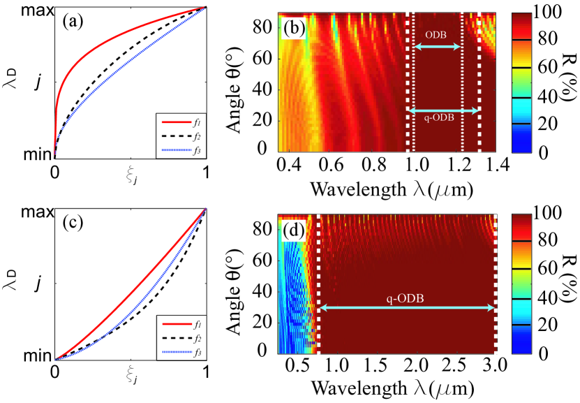
In Fig. 2(a) we present the calculated and measured reflectance for non-polarized light corresponding to sample in the spectral range from 350 to 1400 nm for different angles of incidence , , , , , and . The spectra are qualitatively similar, and for nm and , they agree quantitatively, with a difference smaller than . The measured reflectance is lower than the calculated one, more so at small wavelengths and large angles. This difference may be partially attributed to the scattering of light due to the roughness present at the sample [43, 30, 29] that we have not taken into account in our theory. Due to the limitations of our spectrophotometer, we couldn’t perform measurements for and thus check the ODB. Nevertheless, our results allow us to conclude that the structure has a quasi-ODB from 980 and 1340 nm.
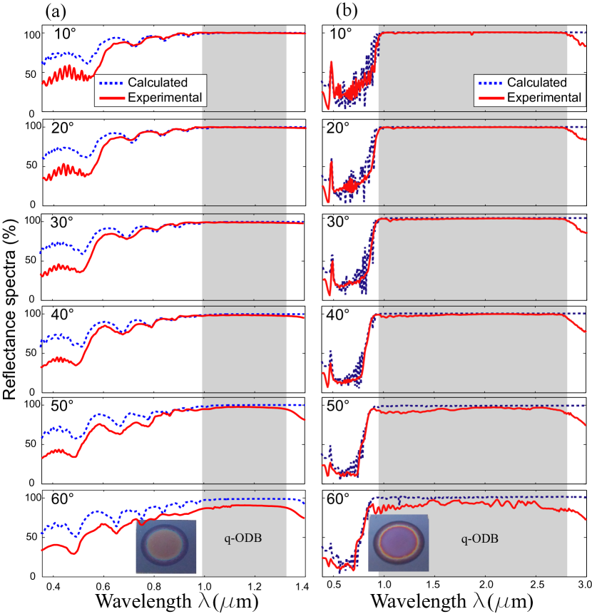
In Fig. 2(b) we compare the calculated and measured spectra of sample in the range from 400 to 3000 nm. Both spectra are very similar, with some differences at long wavelengths which can be attributed to an increase of imperfections such as wavy layers and more roughness for deeper layers, due to a more restricted diffusivity of the electrolyte as the thickness of the structure is increased [44, 45]. According to our results, this structure has a wide quasi-ODW of 1800 nm centered at 1880 nm.
4.2 Photonic structure with sub-mirrors stacking
Another class of techniques for designing good reflectors across a wide spectral range is to stack sub-mirrors tuned to different wavelengths chosen with different criteria. For example, Agarwal et al. [46] proposed a photonic structure in which 54 sub-mirrors were stacked as follows: the first sub-mirror consisted of 2.5 periods tuned to nm; the following -th sub-mirrors were tuned to wavelengths according to the sequence nm with 4 periods for each of the following periods. Furthermore, Estrada-Wiese et al. [47] developed a method that combines three stochastic optimization algorithms together with a narrow space search methodology to obtain a customized and optimized PC configuration.
We recall that for a periodic structure, the propagation of electromagnetic waves is described by the dispersion relation
| (7) |
where is Bloch’s vector and the transfer matrix of a single period of thickness [28, 48, 49]. Thus, whenever electromagnetic energy cannot propagate in the periodic system. This condition corresponds to a photonic band gap within which we expect a high reflectance, even for a finite system made of only a few periods. This suggests the following design strategy. We stack sub-mirrors each made of a few periods of a periodic system such that its photonic band gap (PBG) overlaps the PBG of the previous and that of the next sub-mirror. The number of periods of each sub-mirror is an important parameter. If it is too small, the sub-mirror would be partially transparent within the PBG. If it is too large, the resulting structure would be too thick. This is particularly important for sub-mirrors tuned to shorter wavelengths, for which there is some absorption. We followed thus two design strategies: In the first, we considered sub-mirrors each with the same number of periods. In the second, a different number of periods was assigned to each sub-mirror according to the center of its PBG: we chose a single period for those sub-mirrors tuned to nm, two periods for nm, three periods for nm, and for nm the number of periods was varied between 4 and 10. In both designs, the degree of overlap of consecutive PBGs was taken as the parameter to be optimized in order to maximize the reflectance averaged within the spectral and angular range and for . We define the percentage of overlap in terms of the portion of the PBG of the -th mirror that lies within the PBG of the -th mirror.
Table 2 shows the optimized values of the average reflectance for different choices of the number of periods of each sub-mirror, as discussed above, including the resulting number of stacked sub mirrors, the thickness of the structure, and the optimal overlap of consecutive PBGs. The first and second blocks correspond to the first and second strategies discussed above.
| % overlap | ||||
| 1 | 98 | 43.2 | 95 | 91.0 |
| 3 | 31 | 42.5 | 81 | 91.8 |
| 5 | 17 | 41.9 | 68 | 92.0 |
| 4 | 25 | 38.7 | 74 | 92.3 |
| 6 | 18 | 41.5 | 78 | 95.4 |
| 10 | 13 | 45.4 | 56 | 95.3 |
According to table 2, the structure that has the highest reflectance is in the second block, with an optimal overlap between consecutive PBGs of , a thickness of 41.5 m, and an average reflectance . It is made up of 18 sub-mirrors tuned to the wavelengths 400, 460, 510, 570, 640, 720, 810, 910, 1020, 1150, 1290, 1450, 1630, 1830, 2060, 2320, 2610, and 2860 nm. We synthesized this structure and designated it sample . Its calculated and measured reflectance spectra are shown in Fig. 3.
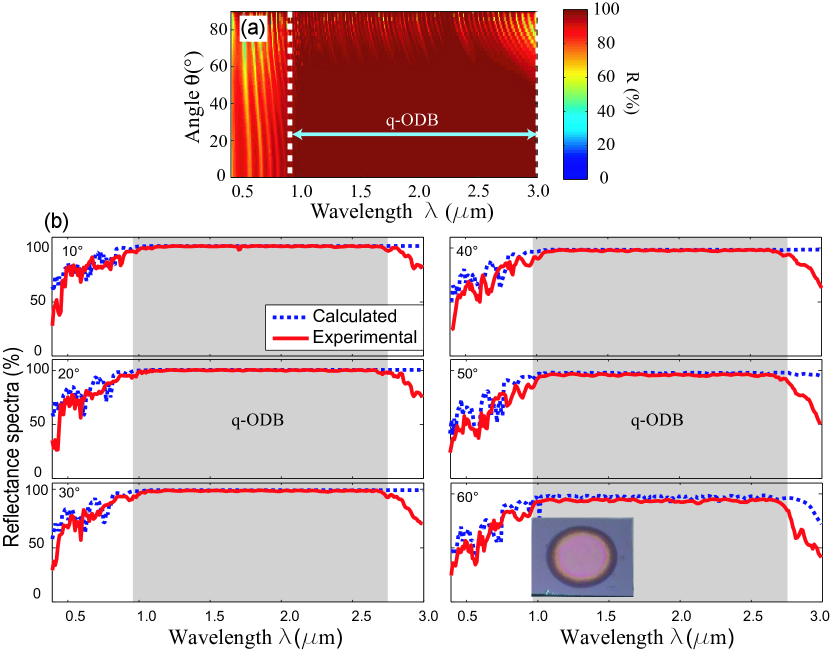
Fig. 3(a) reveals a quasi-ODM in the range from 950 to 2900 nm, with an angular range between and . It is also observed that at incidence angles and long wavelengths the reflectance decreases and has oscillations, which we attribute to the greater penetration of the electromagnetic field within the structure, as shown by Puente-Díaz, et al. [31]. In Fig. 3(b) we compare the calculated and measured reflectance for the structure at several angles of incidence. Although, the quasi omnidirectional wavelength range of the synthesized structure, from 950 to 2750 nm, is slightly smaller than the calculated one, the measured PBG is almost twice as wide as a recently reported PS chirped structure [30], which has the largest previously reported ODW.
Finally, Table 3 shows data from some porous silicon based ODM designed to operate in the NIR region and their of the ODB’s are compared with those of the structures analyzed in the present study. The ODW of the structure results 20 nm wider than that reported by Bruyant, et al. [25] and it is located closer to the visible range. Furthermore, the ODB of the structure begins at 950 nm like the one synthesized by Estevez, et al. [14]; nevertheless, its width extends to 2750 nm. In other words, has an ODW 3.55 times higher. Moreover, the ODW of the structure reported by Xifre-Perez, et al. [50] represents only 17.6 % of the ODW of our and structures. Aditionally, the table reveals that the porous silicon based structures and have the widest gap widths, 1.36 times greater than the largest reported work until now in the NIR region [20]. As compared to the previous studies [25, 14, 50, 20, 51], this work opens the possibility of generating dielectric multilayered structure with large omnidirectional band with the materials with relatively low refractive index contrast.
| Reference | Year | Sample | ODB (nm) | ODW (nm) |
| Bruyant, et al. [25] | 2003 | - | 1100-1440 | 340 |
| Xifre-Pérez, et al. [50] | 2004 | - | 1297-1615 | 318 |
| Estevez, et al. [14] | 2009 | - | 950-1456 | 506 |
| Chavez, et al. [30] | 2020 | - | 1000-2000 | 1000 |
| Wu, et al. [20] | 2021 | - | 1284-2605 | 1321 |
| 980-1340 | 360 | |||
| This work | 2021 | 980-2780 | 1800 | |
| 950-2750 | 1800 |
5 Conclusion
We have designed, optimized, fabricated and characterized highly reflective quasi omnidirectional (angular range of ) multilayered structures with a wide spectral range. Two techniques, chirping (a continuous change in thicknesses) and stacking of Bragg-type sub-structures, have been used to enhance the reflectance with minimum thickness for a given pair of refractive indices. Numerical calculations were carried out employing the transfer matrix method and we optimized the design parameters to obtain maximal reflectance averaged over different spectral ranges for all angles. We fabricated some of the optimized structures with porous silicon dielectric multilayers with low refractive contrast and compared their measured optical properties with the calculations. Two chirped structures with thicknesses 21.6 m and 60.4 m, resulting in quasi omnidirectional mirrors with bandwidths of 360 nm and 1800 nm, centered at 1160 nm and 1925 nm respectively have been shown. In addition, we fabricated a stacked sub-Bragg mirror structure with a quasi omnidirectional bandwidth of 1800 nm (centered at 1850 nm) and a thickness of 41.5 m, which is almost two third (in thickness) of the chirped structure. Thus, our techniques allowed us to obtain relatively thin quasi-omnidirectional mirrors with wide bands over different wavelength ranges. Our analysis techniques can be used for the optimization of the reflectance not only in multilayered PS systems with different refractive index contrasts but also for systems with other types of materials with low refractive index contrast. The present study could also be useful for obtaining omnidirectional dielectric mirrors in large spectral regions using different materials, flat focusing reflectors, thermal regulators, or, if defects are included, as filters or remote chemical/biosensors with a wide angular independent response.
Acknowledgments
This project is supported by Consejo Nacional de Ciencia y Tecnología through grant No.A-S1-30393(VA), 256243 (DA), Cátedras Conacyt program 1577 (DA), and by DGAPA-PAPIIT UNAM under grant IN111119 (LM). VA acknowledges PRODEP (Sabbatical grant), and is grateful to ICF where she spent the sabbatical year. HPA also expresses his gratitude to the Coordinación de la Investigación Científica de la Universidad Michoacana de San Nicolás de Hidalgo. VCG is grateful to CIICAp and ICF where he did this work.
References
- [1] John D. Joannopoulos, Steven G. Johnson, Joshua N. Winn, and Robert D. Meade. Optical Waves in Layered Media Photonic Crystals: Molding the Flow of Light. Princeton University Press, New Jersey, 2nd edition, 2008.
- [2] Amit Kumar Goyal, Hemant Sankar Dutta, and Suchandan Pal. Porous photonic crystal structure for sensing applications. J. Nanophotonics, 12(4):1–7, 2018.
- [3] C. López. Materials Aspects of Photonic Crystals. Adv. Mat., 15(20):1679–1704, 2003.
- [4] Masaya Notomi. Manipulating light with strongly modulated photonic crystals. Rep. Prog. Phys., 73(9):096501, 2010.
- [5] Amit Kumar Goyal and Ajay Kumar. Recent advances and progresses in photonic devices for passive radiative cooling application: A review. J. Nanophotonic, 14(3):1 – 20, 2020.
- [6] R. Szipöcs and A. Koházi-Kis. Theory and design of chirped dielectric laser mirrors. Appl. Phys. B, 65(2):115–135, 1997.
- [7] E. Xifré-Pérez, L. F. Marsal, J. Ferré-Borrull, and J. Pallarés. Low refractive index contrast porous silicon omnidirectional reflectors. Appl. Phys. B, 95(1):169–172, 2009.
- [8] Kevin M. Chen, Andrew W. Sparks, Hsin-Chiao Luan, Desmond R. Lim, Kazumi Wada, and Lionel C. Kimerling. SiO2/TiO2 omnidirectional reflector and microcavity resonator via the sol-gel method. Appl. Phys. Lett., 75(24):3805–3807, 1999.
- [9] Yeonsang Park, Young-Geun Roh, Chi-O Cho, Heonsu Jeon, Min Gyu Sung, and J. C. Woo. GaAs-based near-infrared omnidirectional reflector. Appl. Phys. Lett., 82(17):2770–2772, 2003.
- [10] R. G. DeCorby, H. T. Nguyen, P. K. Dwivedi, and T. J. Clement. Planar omnidirectional reflectors in chalcogenide glass and polymer. Opt. Express, 13(16):6228–6233, 2005.
- [11] S. Jena, R. B. Tokas, S. Tripathi, K. D. Rao, D. V. Udupa, S. Thakur, and N. K. Sahoo. Influence of oxygen partial pressure on microstructure, optical properties, residual stress and laser induced damage threshold of amorphous HfO2 thin films. J. Alloy Compd., 771:373–381, 2019.
- [12] Elisabet Xifré-Pérez, Josep Ferré-Borrull, Josep Pallarés, and Lluís F. Marsal. Methods, Properties and Applications of Porous Silicon. In Dusan Losic and Abel Santos, editors, Electrochemically Engineered Nanoporous Materials: Methods, Properties and Applications, Springer Series in Materials Science, pages 37–63. Springer International Publishing, Cham, 2015.
- [13] O. Bisi, Stefano Ossicini, and L. Pavesi. Porous silicon: a quantum sponge structure for silicon based optoelectronics. Surf. Sci. Rep., 38(1):1 – 126, 2000.
- [14] J. O. Estevez, J. Arriaga, A. Méndez Blas, and V. Agarwal. Enlargement of omnidirectional photonic bandgap in porous silicon dielectric mirrors with a gaussian profile refractive index. Appl. Phys. Lett., 94(6):061914, 2009.
- [15] D. Ariza-Flores, J.S. Pérez-Huerta, Yogesh Kumar, A. Encinas, and V. Agarwal. Design and optimization of antireflecting coatings from nanostructured porous silicon dielectric multilayers. Sol. Energ. Mat. Sol. C., 123:144 – 149, 2014.
- [16] Anne M. Ruminski, Giuseppe Barillaro, Charles Chaffin, and Michael J. Sailor. Internally referenced remote sensors for HF and Cl2 using reactive porous silicon photonic crystals. Adv. Funct. Mat., 21(8):1511–1525, 2011.
- [17] T.V.K. Karthik, L. Martinez, and V. Agarwal. Porous silicon ZnO/SnO2 structures for CO2 detection. J. Alloy Compd., 731:853 – 863, 2018.
- [18] C. P. Hussell and R. V. Ramaswamy. High-index overlay for high reflectance DBR gratings in LiNbO3 channel waveguides. IEEE Photonic Tech. L., 9(5):636–638, 1997.
- [19] E.E. Antunez, J.O. Estevez, J. Campos, M.A. Basurto-Pensado, and V. Agarwal. Formation of photoluminescent n-type macroporous silicon: Effect of magnetic field and lateral electric potential. Physica B, 453:34 – 39, 2014. Low-Dimensional Semiconductor Structures - A part of the XXII International Material Research Congress (IMRC 2013).
- [20] F. Wu, K. Lyu, S. Hu, M. Yao, and S. Xiao. Ultra-large omnidirectional photonic band gaps in one-dimensional ternary photonic crystals composed of plasma, dielectric and hyperbolic metamaterial. Opt. Mater., 111:110680, 2021.
- [21] Volokh Anatoliy, Sergey Marchenko, and Pavel Shestakov. Focusing and defocusing of reflected light beams from chirped dielectric layered structure. In 2017 Days on Diffraction (DD), pages 200–204, 06 2017.
- [22] Yu-Chieh Cheng and Kestutis Staliunas. Near-field flat focusing mirrors. Appl. Phys. Rev., 5(1):011101, 2018.
- [23] María Jimenez Vivanco, Godofredo García, Jesús Carrillo, Vivechana Agarwal, Tomás Díaz-Becerril, Rafael Doti, Jocelyn Faubert, and Eduardo Lugo. Porous Si-SiO2 based UV Microcavities. Sci. Rep.-UK, 10:2220, 12 2020.
- [24] A. David Ariza-Flores, L. M. Gaggero-Sager, and V. Agarwal. White metal-like omnidirectional mirror from porous silicon dielectric multilayers. Appl. Phys. Lett., 101(3):031119, 2012.
- [25] A. Bruyant, G. Lérondel, P. J. Reece, and M. Gal. All-silicon omnidirectional mirrors based on one-dimensional photonic crystals. Appl. Phys. Lett., 82(19):3227–3229, 2003.
- [26] Rolando Perez-Alvarez and F. García-Moliner. Transfer matrix, Green Function and related techniques: Tools for the study of multilayer heterostructures. Universitat Jaume I, España, 01 2004.
- [27] Pochi Yeh. Optical Waves in Layered Media. Wiley, USA, 2nd edition, 2005.
- [28] Mochán W. Luis., del Castillo-Mussot Marcelo., and Barrera Rubén G. Effect of plasma waves on the optical properties of metal-insulator superlattices. Phys. Rev. B, 35(3):1088–1098, 1987.
- [29] Leandro L. Missoni, Guillermo P. Ortiz, María Luz Martínez Ricci, Victor J. Toranzos, and W. Luis Mochán. Rough 1D photonic crystals: A transfer matrix approach. Opt. Mater., 109:110012, 2020.
- [30] B. A. Chavez-Castillo, J. S. Pérez-Huerta, J. Madrigal-Melchor, S. Amador-Alvarado, I. A. Sustaita-Torres, V. Agarwal, and D. Ariza-Flores. A wide band porous silicon omnidirectional mirror for the near infrared range. J. Appl. Phys., 127(20):203106, 2020.
- [31] Luis Eduardo Puente-Díaz, Victor Castillo-Gallardo, Guillermo P. Ortiz, José Samuel Pérez-Huerta, Héctor Pérez-Aguilar, Vivechana Agarwal, and W. Luis Mochán. Stable calculation of optical properties of large non-periodic dissipative multilayered systems. Superlattice Microst., 145:106629, 2020.
- [32] Andrea Edit Pap, Krisztián Kordás, Jouko Vähäkangas, Antti Uusimäki, Seppo Leppävuori, Laurent Pilon, and Sándor Szatmári. Optical properties of porous silicon. Part III: Comparison of experimental and theoretical results. Opt. Mater., 28(5):506–513, 2006.
- [33] D. Estrada-Wiese and J.A. del RÃo. Refractive index evaluation of porous silicon using bragg reflectors. Rev. Mex. Fís., 64:72–81, 02 2018.
- [34] L. T. Canham. Silicon quantum wire array fabrication by electrochemical and chemical dissolution of wafers. Appl. Phys. Lett., 57(10):1046–1048, 1990. Publisher: American Institute of Physics.
- [35] Escorcia J. and Agarwal V. Effect of duty cycle and frequency on the morphology of porous silicon formed by alternating square pulse anodic etching. Phys. Stat. Sol., 4(6):2039–2043, 2007.
- [36] Ariza-Flores A. David, Gaggero-Sager L. M., and Agarwal V. Effect of interface gradient on the optical properties of multilayered porous silicon photonic structures. J. Phys. D: Appl. Phys., 44(15):155102, 2011.
- [37] F. James. MINUIT Function Minimization and Error Analysis: Reference Manual Version 94.1. CERN Program Library Long Writeup D506, 1994.
- [38] K. Glazebrook, J. Brinchmann, C. DeForest J. Cerney, D. Hunt, T. Jenness, T. Lukka, R. Schwebel, and C. Soeller. Perl Data Language (PDL), 1997.
- [39] R.E. Bird, R.L. Hulstrom, and L.J. Lewis. Terrestrial solar spectral data sets. Solar Energy, 30(6):563–573, 1983.
- [40] J. Xu, Q. Sun, Z. Wu, L. Guo, S. Xie, Q. Huang, and Q. Peng. Development of broad-band high-reflectivity multilayer film for positron emission tomography system. Journal of Instrumentation, 13(09):P09016–P09016, 2018.
- [41] Kamal Ahmed, A Khan, A Rauf, and Amir Gul. Multilayer dielectric narrow band mangin mirror. IOP Conference Series: Materials Science and Engineering, 60:012016, 2014.
- [42] Reiner Dietsch, Stefan Braun, Thomas Holz, Hermann Mai, Roland Scholz, and Lutz Bruegemann. Multilayer x-ray optics for energies E > 8 keV and their application in x-ray analysis. In Carolyn A. MacDonald and Ali M. Khounsary, editors, Advances in Laboratory-based X-Ray Sources and Optics, volume 4144, pages 137 – 147. International Society for Optics and Photonics, SPIE, 2000.
- [43] W. Theiß, R. Arens-Fischer, M. Arntzen, M.G. Berger, S. Frohnhoff, S. Hilbrich, and M. Wernke. Probing Optical Transitions in Porous Silicon by Reflectance Spectroscopy in the Near Infrared, Visible and UV. MRS Proceedings, 358:435, 1994.
- [44] Luca Dal Negro, Claudio J. Oton, Zeno Gaburro, Lorenzo Pavesi, Patrick Johnson, Ad Lagendijk, Roberto Righini, Marcello Colocci, and Diederik S. Wiersma. Light Transport through the Band-Edge States of Fibonacci Quasicrystals. Phys. Rev. Lett., 90:055501, 2003.
- [45] G. Vincent. Optical properties of porous silicon superlattices. Appl. Phys. Lett., 64(18):2367–2369, 1994.
- [46] V. Agarwal and J. A. del Río. Tailoring the photonic band gap of a porous silicon dielectric mirror. Appl. Phys. Lett., 82(10):1512–1514, 2003.
- [47] D. Estrada-Wiese, Jesus Del Río, and Ehecatl del Rio-Chanona. Stochastic optimization of broadband reflecting photonic structures. Sci. Rep.-UK, 8:1193, 2018.
- [48] W. Luis Mochán and Marcelo del Castillo Mussot. Optics of multilayered conducting systems: Normal modes of periodic superlattices. Phys. Rev. B, 37:6763–6771, 1988.
- [49] Pérez-Huerta J. S., Ariza-Flores D., Castro-García R., Mochán W. L., Ortiz G. P., and Agarwall V. Reflectivity of 1D photonic crystals: A comparison of computational schemes with experimental results. Int. J. Mod. Phys. B, 32(11):1850136, 2018.
- [50] Xifré-Pérez E., Marsal L. F., Pallarés J., and Ferré-Borrull J. Porous silicon mirrors with enlarged omnidirectional band gap. J. Appl. Phys., 97(6):064503, 2005.
- [51] Yoel Fink, Joshua N. Winn, Shanhui Fan, Chiping Chen, Jurgen Michel, John D. Joannopoulos, and Edwin L. Thomas. A dielectric omnidirectional reflector. Science, 282(5394):1679–1682, 1998.