Valley relaxation of resident electrons and holes in a monolayer semiconductor: Dependence on carrier density and the role of substrate-induced disorder
Abstract
Using time-resolved optical Kerr rotation, we measure the low temperature valley dynamics of resident electrons and holes in exfoliated WSe2 monolayers as a systematic function of carrier density. In an effort to reconcile the many disparate timescales of carrier valley dynamics in monolayer semiconductors reported to date, we directly compare the doping-dependent valley relaxation in two electrostatically-gated WSe2 monolayers having different dielectric environments. In a fully-encapsulated structure (hBN/WSe2/hBN, where hBN is hexagonal boron nitride), valley relaxation is found to be monoexponential. The valley relaxation time is quite long (10 s) at low carrier densities, but decreases rapidly to less than 100 ns at high electron or hole densities 2 cm-2. In contrast, in a partially-encapsulated WSe2 monolayer placed directly on silicon dioxide (hBN/WSe2/SiO2), carrier valley relaxation is multi-exponential at low carrier densities. The difference is attributed to environmental disorder from the SiO2 substrate. Unexpectedly, very small out-of-plane magnetic fields can increase , especially in the hBN/WSe2/SiO2 structure, suggesting that localized states induced by disorder can play an important role in depolarizing spins and mediating the valley relaxation of resident carriers in monolayer transition metal-dichalcogenide semiconductors.
Much of the current excitement surrounding the family of monolayer transition-metal dichalcogenide (TMD) semiconductors such as MoS2 and WSe2 derives from notions of utilizing “valley pseudospin” degrees of freedom as a basis for storing and processing quantum information Xu:2014 ; Schaibley:2016 ; Mak:2018 . Although many of these ideas originated from long-standing considerations of valley degrees of freedom in other materials such as silicon, AlAs, and graphene Shkolnikov:2002 ; Takashina:2006 ; Rycerz:2007 ; Xiao:2007 , monolayer TMD semiconductors have revitalized interests in “valleytronics” due to the ease with which specific valleys in momentum space (namely, the and points in the Brillouin zone) can be selectively populated and probed simply by using/detecting right- or left-circularly polarized light. This convenient set of valley-specific optical selection rules in the monolayer TMDs –which do not exist in most conventional semiconductors or in graphene– arises from their lack of inversion symmetry, and large spin-orbit coupling Yao:2008 ; Xiao:2012 .
Analogous to the keen interest in electron, hole, and exciton spin relaxation during the early days of semiconductor spintronics OO ; SS ; Dyakonovbook , measurements of valley relaxation in monolayer TMDs are currently a focus of attention for potential applications in valleytronics. Considerable initial attention followed from early photoluminescence (PL) studies in 2012 demonstrating that when certain monolayer TMDs were photoexcited by circularly-polarized light, the resulting PL was strongly co-circularly polarized Sallen:2012 ; Zeng:2012 ; Mak:2012 ; Cao:2012 , suggesting that valley degrees of freedom might be especially robust and long-lived. However, because PL necessarily originates from the optical recombination of transient excitons, co-polarized PL is equally consistent with very short exciton lifetimes (i.e., even shorter than the timescale of fast exciton valley scattering). And indeed, very fast exciton and trion PL lifetimes in the 1-100 ps range were subsequently revealed in time-resolved PL studies Wang:2014 ; Robert:2016 ; Wang:2018 .
While the dynamics of excitons and exciton valley scattering in monolayer TMDs Wang:2018 ; Mai:2014 ; Zhu:2014 ; Singh:2016 ; Hao:2016 ; Yu:2014 ; DalConte:2015 ; Yan:2017 ; Plechinger:2016 ; Molina:2017 are surely very important for certain opto-electronic applications, a different and arguably more relevant question for many putative valleytronic applications is: “What are the intrinsic valley relaxation timescales of the resident electrons and holes that exist in -type doped and -type doped TMD monolayers?”. In this case, electron-hole exchange interactions – which can be a very efficient valley scattering and decoherence mechanism for polarized excitons Wang:2018 ; Mai:2014 ; Zhu:2014 ; Singh:2016 ; Hao:2016 ; Yu:2014 ; DalConte:2015 ; Yan:2017 ; Plechinger:2016 ; Molina:2017 – are absent. Therefore, much longer valley relaxation timescales may be expected for resident electrons and holes, because the spin-orbit splitting and resulting spin-valley locking in the conduction bands and in (especially) the valence bands mandates that valley scattering at low temperatures requires not only a large momentum change (), but also a spin flip Xiao:2012 .
Similar to the way in which long spin lifetimes of resident electrons and holes enabled spin-based device demonstrations in conventional semiconductors and graphene Lou:2007 ; Kroutvar:2004 ; Appelbaum:2007 ; Han:2014 , it is therefore the valley relaxation of the resident electrons and holes in doped TMD monolayers and heterostructures that will likely determine the functionality of many valley-based device concepts. To this end, systematic studies of resident carrier valley dynamics in doped TMD monolayers are essential, particularly as a function of carrier density, temperature, and overall material quality.
Experimental studies along these lines commenced in about 2015, typically using polarization-resolved optical pump-probe methods such as time-resolved circular dichroism and Kerr/Faraday rotation – techniques that had been developed and refined in the preceding decades to explore spin lifetimes and spin coherence in conventional III-V and II-VI semiconductors Crooker:1997 ; Greilich:2006 . Initial measurements focused on MoS2, WS2, and WSe2 monolayers grown by chemical vapor deposition (CVD), which were unintentionally doped with either electrons or holes Yang:2015 ; Hsu:2015 ; Song:2016 ; McCormick:2017 . These studies typically revealed multi-exponential valley relaxation with longer timescales on the order of several nanoseconds at low temperatures (i.e., roughly longer than the measured recombination times of the “bright” excitons and trions Wang:2014 ; Robert:2016 , and also the nominally-forbidden “dark” excitons and trions Robert:2017 ; Zhang:2017 ; Liu:2019 ; Molas:2019 ; Chen:2020 ). While very encouraging, the CVD-grown monolayers studied in Yang:2015 ; Hsu:2015 ; Song:2016 ; McCormick:2017 were not charge-adjustable, and moreover they exhibited broad optical absorption lines (many tens of meV) indicating significant inhomogeneous broadening, likely due to the fact that they were grown by CVD, directly on SiO2 or sapphire substrates, with surfaces that were not encapsulated or passivated.
Subsequent studies then focused on carrier valley relaxation in mechanically-exfoliated (but still unpassivated) WSe2 monolayers that exhibited improved optical quality, and which afforded some degree of charge tunability via electrostatic gating Dey:2017 . Here, 100 ns valley relaxation of resident electrons was found in the heavily -type doped regime, while a very long microsecond-duration valley relaxation of holes was observed when the same monolayer was gated -type (although a systematic dependence on carrier density was not performed). Similarly, pump-probe measurements of WSe2/MoS2 bi-layers, in which photoexcited holes quickly migrated to the WSe2 layer and then relaxed independently from the electrons, also showed long microsecond valley relaxation of holes Kim:2017 .
In parallel, at about this time (2017) it became widely appreciated that the optical quality of TMD monolayers could be significantly improved via full encapsulation between slabs of exfoliated hexagonal boron nitride (hBN) Cadiz:2017 ; Ajayi:2017 ; Wang:2017 . This key advance made it possible to achieve TMD monolayers with not only exceptionally narrow (a few meV) exciton linewidths approaching the homogeneous limit, but also with the ability to be continuously gated all the way from the heavily electron-doped regime to the heavily hole-doped regime Wang:2017 ; VanTuan:2019 , likely owing to a reduction of defects, traps, and localized states in the WSe2 forbidden band gap. Using hBN-encapsulated structures, mono-exponential valley relaxation of resident electrons and holes was observed, with timescales of order 100 ns (for electrons) to several microseconds (for holes) Jin:2018 ; Goryca:2019 . Crucially, these long timescales were validated by passive optical detection of the thermodynamic valley fluctuations (‘valley noise’) of the resident carriers in thermal equilibrium (i.e., no pump laser or excitation was used) Goryca:2019 , confirming that the long decays originate from the intrinsic valley relaxation of the resident electrons and holes themselves, and not from, e.g., any type of long-lived dark or trapped exciton Volmer:2017 .
As outlined above, a wide range of electron and hole valley relaxation timescales have been reported to date, which is due in part to the significant improvement in the quality and passivation of TMD monolayers over the past several years, and also because different studies reported on samples with different specific carrier densities. Here, we attempt to provide a more unified understanding of resident carrier valley relaxation in monolayer TMD semiconductors, by directly comparing the detailed doping dependence of valley relaxation in two electrostatically-gated WSe2 monolayers having different surrounding dielectric environments. In a fully-encapsulated WSe2 monolayer (hBN/WSe2/hBN), valley relaxation is found to be almost perfectly monoexponential. The valley relaxation time is quite long (10 s) at low carrier densities, but decreases rapidly to less than 100 ns at high electron or high hole densities exceeding 2 cm-2. In contrast, in a partially-encapsulated WSe2 monolayer placed directly on a silicon dioxide substrate (hBN/WSe2/SiO2) – another common assembly motif – carrier valley relaxation is found to be multi-exponential at low densities, exhibiting a faster initial decay followed by a slow (10 s) relaxation. The difference is attributed to in-gap states in the WSe2 introduced by dielectric disorder in the SiO2 substrate, which has an especially strong influence on monolayer TMDs in the low carrier density regime. Similar to the fully-encapsulated case, however, this slow relaxation accelerates by over two orders of magnitude with increasing electron or hole doping. Increasing temperatures also accelerate valley relaxation, and – crucially – the unexpected influence of small perpendicular magnetic fields is measured and discussed in the context of localized in-gap states that can depolarize spins and thereby mediate carrier valley relaxation.
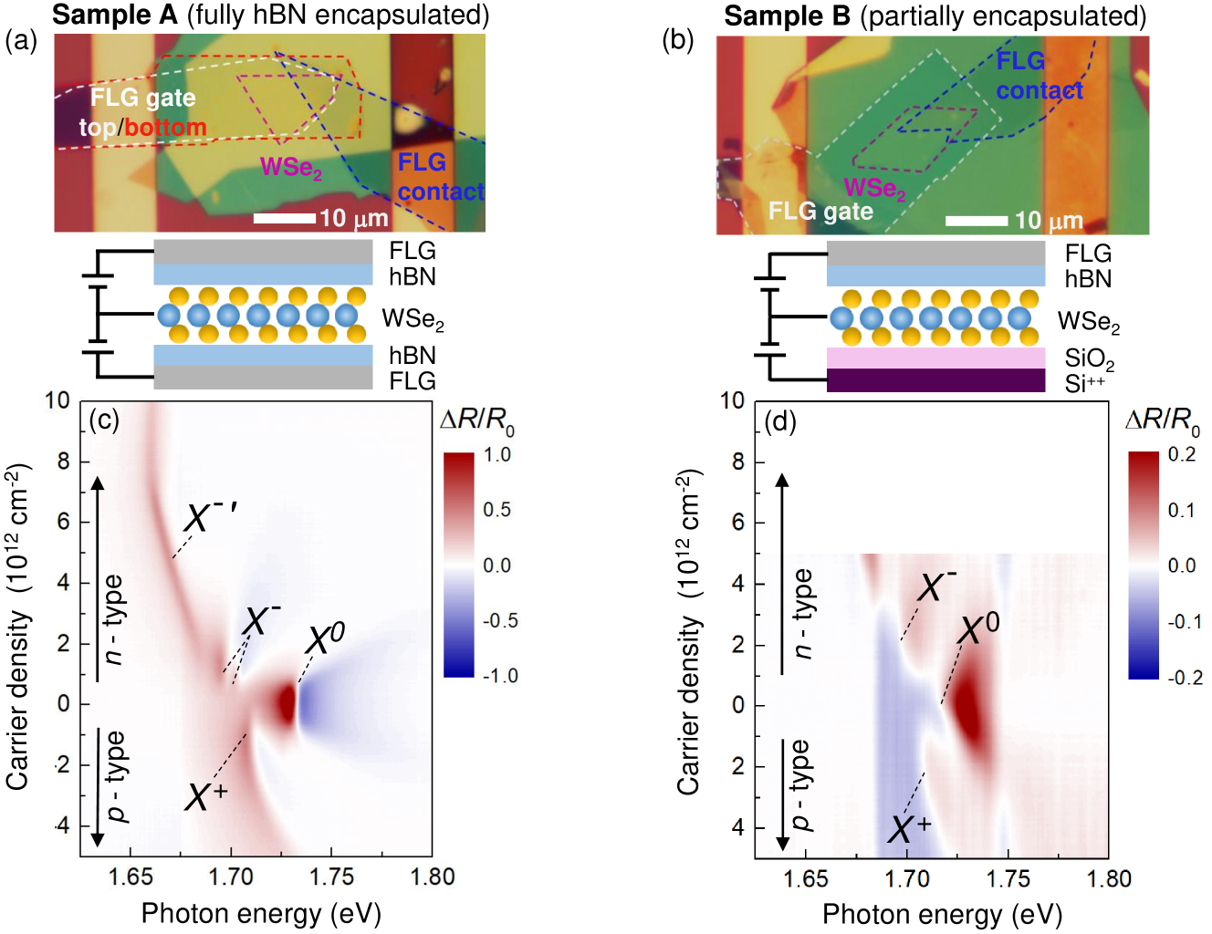
Figure 1 shows the two different electrostatically-gated WSe2 monolayer structures measured in this work. To ensure accurate comparisons, both structures incorporate a single WSe2 monolayer that was mechanically exfoliated from the same high-quality bulk crystal grown by the self-flux method, in which the density of lattice defects is much lower than in bulk crystals grown by chemical vapor transport Edelberg:2019 . Both structures were assembled using the same van der Waals dry stacking method to provide clean interfaces between the WSe2 and its adjacent dielectric materials.
“Sample A” (Fig. 1a) is representative of modern structures exhibiting very high optical quality: it is a fully hBN-encapsulated WSe2 monolayer (hBN/WSe2/hBN), with top/bottom gates and a contact electrode made from flakes of few-layer graphite (FLG). Here, the complete encapsulation by pristine (not post-processed) exfoliated hBN flakes provides an atomically-smooth and largely defect-free dielectric environment Dean:2010 entirely surrounding the WSe2 monolayer, which leads to very narrow features in optical spectra, as discussed below. Full hBN encapsulation is now widely recognized to yield monolayer TMD structures with excellent optical properties and a minimum of inhomogeneous broadening and disorder Cadiz:2017 ; Ajayi:2017 ; Raja:2019 ; Rhodes:2019 ; Martin:2020 .
In contrast, “Sample B” (Fig. 1b) is representative of a different, but nonetheless very common, type of van der Waals structure: it is a partially-encapsulated WSe2 monolayer that is placed directly on silicon dioxide (hBN/WSe2/SiO2). Here, gating is achieved via a top FLG gate electrode and the underlying heavily-doped Si substrate. In this case, the WSe2 monolayer is in direct contact with the SiO2, and is therefore in intimate proximity to surface defects, dangling bonds, dielectric disorder, and surface roughness, with a consequent reduction in the optical quality of the TMD monolayer.
The difference in optical and material properties between the two structures is readily apparent in the gate-dependent maps of optical reflectivity, shown in Figs. 1(c,d). These maps show normalized reflection spectra () acquired at low temperature (5.8 K), as the resident carrier density in the WSe2 monolayers is tuned from heavily electron doped (-type), to nominally undoped (charge neutral), to heavily hole doped (-type). For clarity, throughout this paper we use “” and “” when referring to electron and hole densities, respectively. High electron densities () and high hole densities () exceeding cm-2 are achieved in both structures, thanks to the dual-gating configuration. Importantly, no hysteresis as a function of gate voltage or slow drifts were observed in the measured optical properties of the WSe2 JingLi:2020 , likely due to the use of pristine (never post-processed) hBN encapsulation layers, and because (in sample B) the bottom Si++ gate voltage is never varied.
In the fully-encapsulated sample A (Fig. 1c), a series of sharp exciton resonances are observed as a function of carrier density. The neutral exciton resonance () at 1.733 eV appears only in a narrow gating region around the charge neutrality point. When and exceed 0.3 cm-2, strong negatively-charged exciton () and positively-charged exciton () resonances appear, respectively, at 1.700 eV and 1.710 eV. The appearance of charged excitons (also called ‘trions’ or ‘attractive polarons’ in the literature) in optical reflectivity spectra indicates a substantive change in the available joint density of states of the WSe2 monolayer, and therefore the absorption oscillator strength, that is due to the occupation of the conduction bands (CB) and valence bands (VB) by resident carriers. At large electron doping ( cm-2), an additional resonance appears at lower energy, which further redshifts with increasing . Although the nature of this resonance is not yet fully understood VanTuan:2017 ; Wang:2017 , in keeping with recent studies we label this peak as . Importantly, these reflectivity spectra are in excellent agreement with other recent measurements of gate-dependent absorption and reflection of hBN-encapsulated WSe2 monolayers Wang:2017 ; VanTuan:2019 .
In the partially-encapsulated sample B (Fig. 1d), we observe a qualitatively similar dependence of on carrier density. However, the exciton resonances are spectrally much broader and weaker (note the different intensity scale). The neutral exciton is clearly visible near the charge neutrality point, but is spectrally broad (35 meV, versus 6 meV in the sample A). charged exciton features are also broader, and do not appear until the carrier density exceeds 1 cm-2, suggesting the presence of ample states in the nominally forbidden band gap of the WSe2 monolayer, likely introduced by the close proximity to the SiO2 substrate.
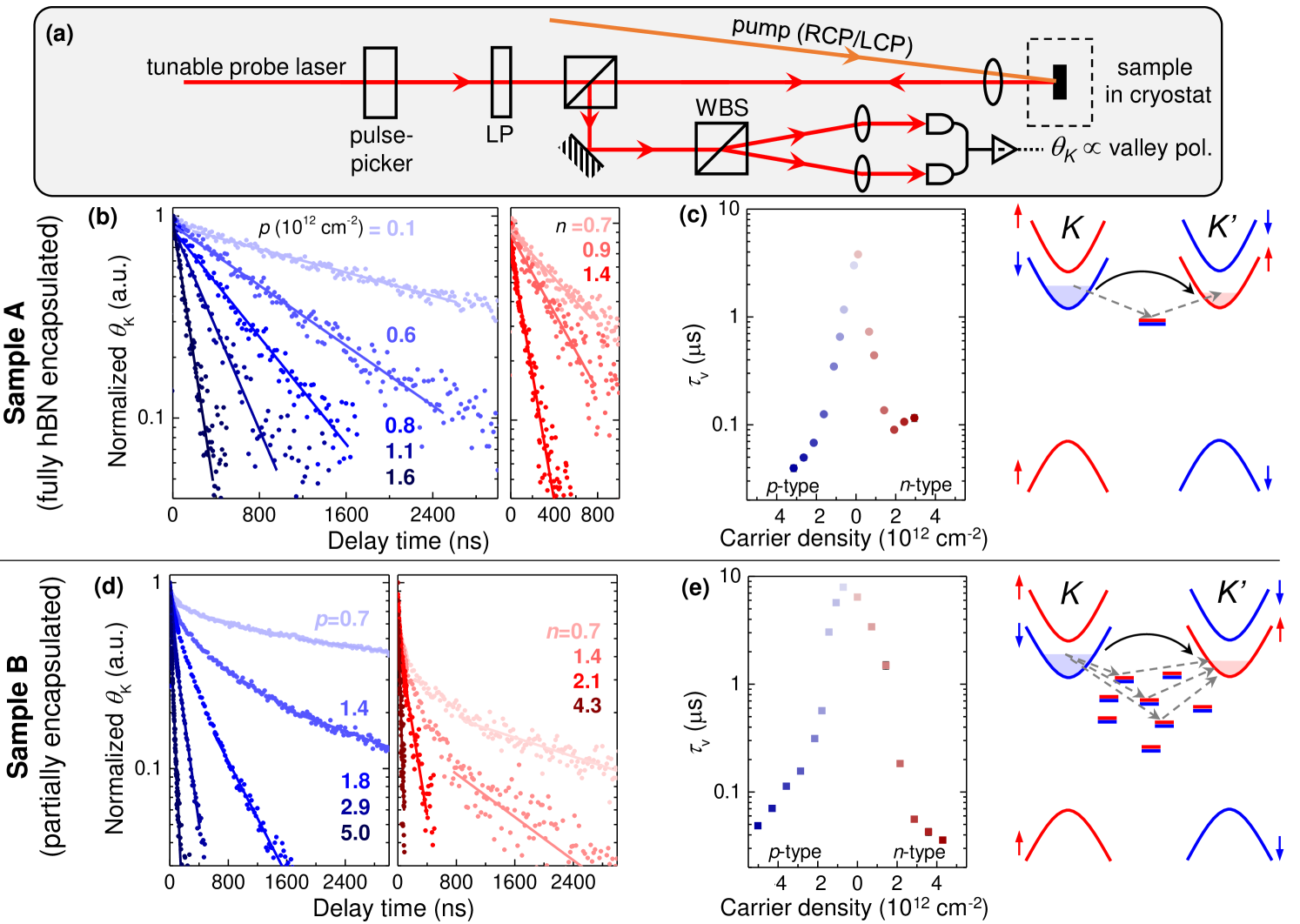
Figure 2(a) depicts the time-resolved Kerr rotation (TRKR) experiment that was used to measure the valley dynamics of the resident carriers. The gated WSe2 structures were mounted on the cold finger of a small optical cryostat. A pulsed diode laser generated short (80 ps) optical pump pulses at 645 nm (1.922 eV), which were then circularly polarized and focused to a 10 m diameter spot on the sample. Owing to the valley-specific optical selection rules in monolayer WSe2, the above-gap pump photoexcites valley- and spin-polarized electrons and holes into the monolayer, which rapidly relax to the band edges and form bright and dark excitons and trions, which subsequently scatter and recombine on short (1 ns) timescales Wang:2014 ; Robert:2016 ; Robert:2017 ; Zhang:2017 ; Liu:2019 ; Molas:2019 ; Chen:2020 ; Wang:2018 . Invariably, some of the possible recombination pathways involved phonon-assisted transitions, nonradiative recombination, and the existing resident carriers – the net effect of which induces a nonequilibrium spin/valley polarization to the Fermi sea of resident carriers.
The subsequent relaxation of this pump-induced valley polarization on timescales longer than a few hundred picoseconds was detected via the optical Kerr rotation imparted on time-delayed and linearly-polarized probe pulses (150 fs) from a wavelength-tunable Ti:sapphire laser focused to a small 3 m diameter spot on the sample. To enable the accurate and unambiguous measurement of the long (0.1-10 s) valley relaxation observed in this work, it was necessary to reduce the repetition rate of the Ti:sapphire laser by an acousto-optic pulse-picker, so that the time interval between excitation cycles was longer than the measured relaxation time. The time delay between the pump and probe pulses was synchronized and controlled by an electronic timing delay Dey:2017 . The pump pulses were modulated between right- and left-circular polarization by a photoelastic modulator, and the pump-induced Kerr rotation was detected by balanced photodiodes and measured via standard lock-in techniques. The probe laser was typically tuned in photon energy to the peak of the induced Kerr response, which coincided with the spectral position of the charged exciton resonances, as discussed in more detail below.
The carrier-density-dependent valley relaxation in both samples is shown in Figs. 2(b-e). Red-shaded and blue-shaded traces show measured decays of in the electron-doped (-type) and hole-doped (-type) regimes, respectively. In the fully-encapsulated sample A, was observed to decay almost perfectly mono-exponentially at all carrier densities (Fig. 2b), suggesting that a single relaxation mechanism dominates. We note that monoexponential decays were also observed in recent time-resolved studies of carrier valley dynamics in high-quality (fully hBN encapsulated) structures Goryca:2019 ; Jin:2018 . The valley lifetime that we observe in sample A is very long at low carrier density (several microseconds), in agreement with recent time-resolved measurements Dey:2017 ; Goryca:2019 ; Jin:2018 ; Kim:2017 . However, we find that drops precipitously with increasing electron or hole doping, to values on the order of 100 ns at high electron or high hole densities cm-2. We emphasize that even this comparatively rapid decay (100 ns) is still approximately 2-3 orders of magnitude longer than the measured recombination time scales of dark excitons and trions (0.1-1 ns) in monolayer WSe2 Robert:2017 ; Zhang:2017 ; Liu:2019 ; Molas:2019 ; Chen:2020 , strongly supporting its interpretation as the slow valley relaxation of resident carriers. The complete set of measured valley lifetimes in sample A as a function of resident carrier density are summarized in Fig. 2c. As just described, exhibits a sharp maximum at low carrier density.
In contrast, valley dynamics in the partially-encapsulated sample B (Fig. 2c) are found to be multi-exponential, especially at lower carrier densities below 2 cm-2, suggesting multiple relaxation mechanisms at play. In this low-density regime, a faster initial relaxation is typically followed by a slower and nearly mono-exponential decay. These multi-exponential decays are similar to time-resolved measurements reported in early studies of CVD-grown and/or unencapsulated TMD monolayers having broader exciton linewidths and reduced optical quality Yang:2015 ; Hsu:2015 ; Song:2016 ; McCormick:2017 . We associate the slower decay at long time delays with the intrinsic valley relaxation time , and again find long valley depolarization on the order of 10 s at low carrier densities (i.e., similar to sample A). However, accelerates by over two orders of magnitude with increasing - and -type doping, again similar to sample A (moreover, we note that valley relaxation becomes more closely mono-exponential). The dependence of on carrier density in sample B (Fig. 2e) roughly follows that observed in sample A (Fig. 2c), although its decrease with and is less abrupt.
We emphasize that samples A and B were fabricated using identical WSe2, hBN, and graphite source materials, the same mechanical exfoliation protocol, and the same van der Waals dry-stacking setup and process. Therefore we associate the qualitatively different carrier valley dynamics observed in sample B (that is, multi-exponential decay) to an extrinsic origin, likely due to dielectric disorder and inhomogeneity introduced by the underlying SiO2. Because SiO2 is a convenient and common substrate for a variety of 2D material platforms, these disorder potentials and related deleterious effects have been studied carefully over the past years, particularly in relation to the properties of SiO2-supported graphene Zhang:2009 ; Dean:2010 ; Decker:2011 , and more recently in relation to the optical and electronic properties of TMD monolayers Shin:2016 ; Borys:2017 ; Raja:2019 ; Rhodes:2019 . For example, scanning tunneling microscopy studies Shin:2016 revealed charge puddles in TMD monolayers on SiO2, wherein the energies of the conduction band minima and valence band maxima varied by hundreds of meV over lateral length scales of order 10 nm. In comparison, pristine hBN provides a largely defect- and inhomogeneity-free platform for both graphene and TMD monolayers Dean:2010 ; Decker:2011 ; Rhodes:2019 . As we discuss in more detail below, our time-resolved measurements of carrier valley depolarization in monolayer WSe2 are consistent with a larger degree of inhomogeneity in the SiO2-supported sample B, and the formation of localized in-gap states arising from this environmental disorder, which in turn can play a role in depolarizing spins and mediating valley relaxation.
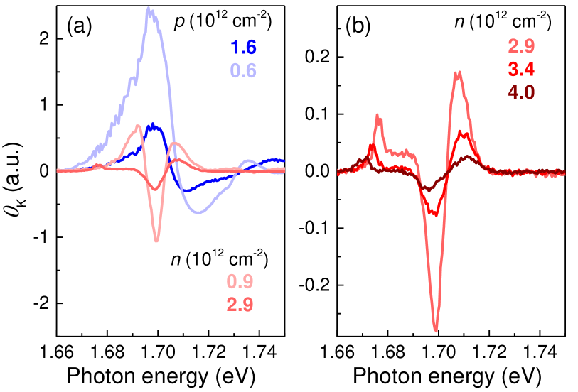
Before turning to the role of substrate-induced disorder, we discuss the spectral dependence of the measured Kerr rotation signals. As noted above, all the TRKR measurements were performed using above-gap pump pulses with fixed wavelength (645 nm, or 1.922 eV), while the probe pulses were tuned in wavelength near the peak of the induced Kerr-rotation response, which occurs in the spectral vicinity of the and charged exciton resonances. For completeness, the full spectral dependence of the induced Kerr response from sample A is shown in Fig. 3, at different representative electron and hole densities. Here, the experiment is essentially the same as for TRKR (see Fig. 2a), except that the pump diode laser and the tunable probe laser are now operated in continuous-wave (cw) mode. Thus, the measured is the induced Kerr rotation in response to a small steady-state (but still non-equilibrium) valley polarization of the resident carriers comprising the Fermi sea.
In our experience, a comprehensive understanding of the absorption spectrum and the optically-induced Kerr spectrum is essential in studies of this type. This is because, as can be seen from Fig. 3, relatively small variations of probe laser’s photon energy with respect to the system’s underlying absorption resonances can result in Kerr signals having significantly different magnitude and even opposite sign (although measured timescales are typically not affected, provided the signals derive from the same absorption resonance). Changes in signal magnitude and sign may arise trivially, due for example to exciton resonances that shift in energy (with respect to a fixed probe laser) as a function of temperature or carrier density or strain. The spectra in Fig. 3 show that the optically-induced Kerr response exhibits a clear dispersive antisymmetric resonance centered near 1.71 eV, which coincides with the spectral position of the and charged exciton resonances (cf. Fig. 1). As discussed and shown previously Dey:2017 ; Goryca:2019 , this behavior is in line with expectations: a non-zero valley polarization of resident carriers is anticipated to manifest most prominently in the circular polarization of the bright charged exciton resonances, since the very existence of charged excitons depends explicitly of the presence of resident carriers in the monolayer.
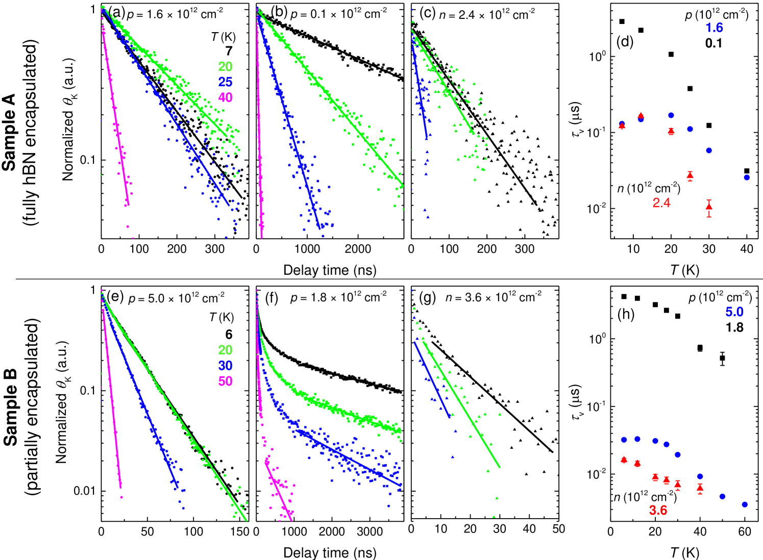
Figure 4 shows how the measured carrier valley relaxation changes with temperature (up to 50 K), at various densities, in both samples A and B. Overall, decreases as temperature increases, and qualitatively similar temperature-dependent trends were also observed in previous studies of carrier valley relaxation Yang:2015 ; Song:2016 ; Kim:2017 ; Goryca:2019 ; Ersfeld:2020 . We note, however, that while varies significantly with temperature at very low doping (in sample A), it is relatively insensitive to temperatures 20 K at higher carrier densities (e.g., cm-2, or cm-2, as shown in Figs. 4a and 4c.). In contrast, in sample B exhibits a marked temperature dependence over a wider range of carrier densities. In general, temperature-dependent valley relaxation of resident carriers can be expected if carrier-phonon interactions promote spin-flip intervalley scattering Molina:2017 ; Ochoa:2013 ; Song:2013 ; Gunst:2016 , either directly or via Elliot-Yafet and Dyakonov-Perel spin relaxation mechanisms WangWu:2014 ; Ochoa:2014 , which have recently been reevaluated using ab initio methods for 2D materials lacking spatial inversion symmetry Xu:2020 .
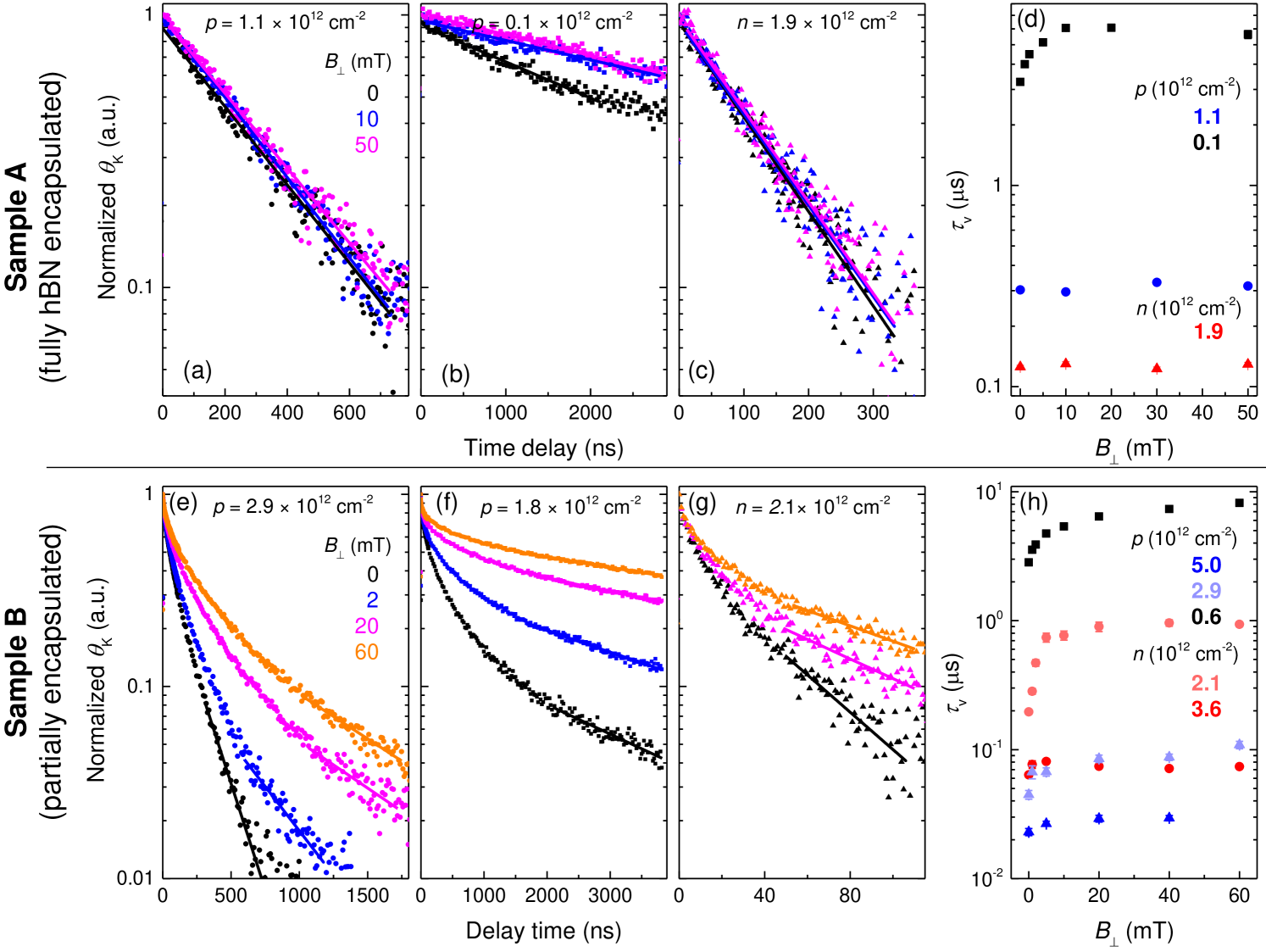
Small applied magnetic fields provide important additional insight. Figure 5 shows measured in both samples A and B, at low temperature (5.8 K), as a function of small applied out-of-plane magnetic field up to 50 mT. In sample A, is insensitive to field except at very small carrier densities (e.g., as shown in Fig. 5b where cm-2), where approximately doubles, but then saturates by 10 mT. For larger electron or hole doping, is insensitive to (see Figs. 5a and 5c). In marked contrast, in sample B both and the overall valley decays show a considerable variation with at all measured electron and hole carrier densities – and in particular, the faster component is rapidly suppressed with [see Figs. 5(e-g)].
The sensitivity of to small is perhaps somewhat surprising in view of the large spin-orbit splittings that exist between spin-up and spin-down conduction bands ( meV) and valence bands ( meV) at the points in monolayer WSe2. and impose huge out-of-plane effective magnetic fields in the range of T that are ‘seen’ by electrons and holes residing at the and points of the Brillouin zone. As such, the addition of small mT should be insignificant in comparison. The experimental fact that small does strongly influence (at the lowest carrier densities in sample A, and over a wider density range in sample B) therefore suggests that some population of intermediate in-gap states likely participates in the valley relaxation process – and moreover, that these states are not subject to the huge effective spin-orbit magnetic fields in monolayer TMDs, possibly because they lack the inversion-asymmetric crystal symmetry of the host lattice Kaasbjerg:2017 ; Abramson:2018 . Such states would have nearly degenerate spin levels. A potential valley relaxation pathway can therefore arise if a spin-polarized carrier from (say) the valley scatters to an in-gap state and subsequently precesses about any residual in-plane effective magnetic field, and then scatters to the valley when its spin projection has reversed.
We note that a related intermediate-state mechanism was recently proposed to account for the circular polarization of PL from low-energy defect states in monolayer WSe2 Smolenski:2016 , which was found to be similarly sensitive to small . As also noted in Smolenski:2016 , the sensitivity to small applied is reminiscent of early optical orientation studies of spin-polarized resident electrons in -type GaAs OO ; Furis:2007 , when small in-plane effective magnetic fields were present due to Rashba or strain-related spin-orbit coupling. While such in-plane effective fields can depolarize out-of-plane oriented spins by inducing spin precession, their influence is readily suppressed by application of , which stabilizes out-of-plane spin orientation.
Taken together, the measured dependence of on carrier density, encapsulation, temperature, and are consistent with a picture of electron/hole valley relaxation shown in the diagrams in Figure 2. Once a valley polarization of the resident carriers is established by the pump pulse (following rapid exciton scattering and recombination on short timescales), the resident carrier polarization can relax either via intrinsic pathways related to density- and temperature-dependent carrier-phonon coupling, and associated Dyakonov-Perel and Elliott-Yafet mechanisms (solid lines) Song:2013 ; Gunst:2016 ; Ochoa:2014 ; WangWu:2014 ; Xu:2020 , or it can also relax via extrinsic pathways (dotted lines) mediated by a population of in-gap states that exist due to localized defects Kaasbjerg:2017 ; Abramson:2018 or to the disorder potential arising from an imperfect underlying substrate. If, as the dependence on suggests, these in-gap states are not subject to the huge perpendicular effective magnetic fields from Kaasbjerg:2017 ; Abramson:2018 , then spin degrees of freedom at these localized sites are nearly degenerate and spins can depolarize due to precession about any residual effective fields, thereby mediating alternative relaxation pathways between the spin-valley locked carriers at and , in a two-step process depicted by the dotted lines. Note that in early studies of unpassivated CVD-grown TMD monolayers having significant disorder, evidence for a localized sub-population of carriers exhibiting free spin precession at a frequency proportional only to an applied transverse field (i.e., no evidence of any large effective spin-orbit field) was reported in Yang_NL:2015 and McCormick:2017 ; Volmer:2017 by TRKR methods.
We argue that in lower-quality TMD monolayers such as sample B (which is in direct contact with SiO2), in-gap states are likely more numerous and are more broadly distributed in energy – and therefore play a more prominent role – as compared with fully-encapsulated high-quality monolayers such as sample A. Furthermore, an ensemble of in-gap states can be expected to play a more dominant role at low carrier densities when their distribution is only partially occupied, and a less important role at high carrier densities when they are full. This is consistent with the data shown in Fig. 2, where the multiexponential decays observed in sample B are most clearly evident at low electron and hole densities, but at higher carrier densities when in-gap states fill, the decays become more closely monoexponential (and also faster, as density-dependent intrinsic mechanisms begin to dominate). In comparison, the fully-encapsulated sample A exhibits monoexponential decays at all carrier densities, suggesting mostly intrinsic mechanisms at play.
Consequently, and in summary, the data therefore suggest that the marked carrier density dependence of in sample A – which drops by over two orders of magnitude from 10 s at low density to 100 ns when cm-2 (see Fig. 2c) – is likely an intrinsic effect, due to a Fermi energy (and momentum) -dependent valley relaxation in monolayer TMDs. It is interesting that both electron and hole doping have such similar effects on ; however, at the carrier densities and low temperatures (5.8 K) at which this study was performed, both the Fermi energy (15 meV) and the thermal energy ( meV) are always less than the spin-orbit splitting of the conduction bands in WSe2 ( meV). The surprising dependence of on small out-of-plane magnetic fields provides additional key insight, both by revealing the likely presence of intermediate in-gap states having negligible (or small in-plane) spin-orbit effective fields that can mix spins via precession and thereby mediate intervalley relaxation, and also by providing a simple means to suppress their influence so that intrinsic mechanisms can be more clearly revealed, as demonstrated in Fig. 5. Finally, the important role of substrate (dielectric) disorder on the optical properties and the valley relaxation of resident carriers is more clearly revealed by a direct side-by-side comparison of fully- and partially-encapsulated monolayers.
Looking forward, the steady improvement of TMD monolayer material quality and passivation methods can be expected to result in correspondingly enhanced valley lifetimes for resident carriers. The nearly-monoexponential decays observed in sample A, along with the relatively small influence of out-of-plane applied magnetic fields, suggests that intrinsically-limited valley lifetimes are already being approached in fully hBN encapsulated monolayers. An improved theoretical understanding of intrinsic valley relaxation mechanisms, and (especially) the strong temperature dependence and marked dependence on carrier density, will be extremely helpful in this regard. Systematic experimental studies of carrier valley lifetimes in other members of the TMD monolayer family are also warranted, particularly in Mo-based monolayers where the spin-orbit splitting of the conduction band can be much smaller than in their W-based counterparts, such that even low electron density Fermi seas can occupy both spin bands in each valley. Tunable manipulation of valley degrees of freedom for resident electrons and holes remains a significant challenge, but these results suggest a potential route based on intermediate states having different symmetry, at which spin degrees of freedom can in principle be more readily controlled.
Jing Li and M. Goryca contributed equally to this work. We gratefully acknowledge Junho Choi, Cedric Robert, Bernhard Urbaszek, Xavier Marie, and Yuan Ping for helpful discussions. Work at the NHMFL was supported by the Los Alamos LDRD program. The NHMFL was supported by National Science Foundation (NSF) DMR-1644779, the State of Florida, and the U.S. Department of Energy (DOE). S.T. acknowledges support from DOE-SC0020653, Applied Materials Inc., NSF DMR-1955889, NSF CMMI-1933214, NSF 1904716, NSF 1935994, and NSF DMR-1552220.
References
- (1) X. Xu, W. Yao, D. Xiao, and T. F. Heinz, Spin and pseudospins in layered transition metal dichalcogenides, Nat. Phys. 10, 343 (2014).
- (2) J. R. Schaibley, H. Yu, G. Clark, P. Rivera, J. S. Ross, K. L. Seyler, W. Yao, and X. Xu, Valleytronics in 2D materials, Nat. Rev. Mater. 1, 16055 (2016).
- (3) K. F. Mak, D. Xiao, and J. Shan, Light-valley interactions in 2D semiconductors. Nat. Photon. 12, 451 (2018).
- (4) Y. P. Shkolnikov, E. P. De Poortere, E. Tutuc, M. Shayegan, Valley splitting of AlAs two-dimensional electrons in a perpendicular magnetic field, Phys. Rev. Lett. 89, 226805 (2002).
- (5) K. Takashina, Y. Ono, A. Fujiwara, Y. Takahashi, and Y. Hirayama, Valley Polarization in Si(100) at Zero Magnetic Field, Phys. Rev. Lett. 96, 236801 (2006).
- (6) A. Rycerz, J. Tworzydło, C. W. J. Beenakker, Valley filter and valley valve in graphene, Nat. Phys. 3, 172 (2007).
- (7) D. Xiao, W. Yao, and Q. Niu, Valley-contrasting physics in graphene: Magnetic moment and topological transport, Phys. Rev. Lett. 99, 236809 (2007).
- (8) W. Yao, D. Xiao, Q. Niu, Valley-dependent optoelectronics from inversion symmetry breaking, Phys. Rev. B 77, 235406 (2008).
- (9) D. Xiao, G.-B. Liu, W. Feng, X. Xu, and W. Yao, Coupled spin and valley physics in monolayers of MoS2 and other group-VI dichalcogenides, Phys. Rev. Lett. 108, 196802 (2012).
- (10) Optical Orientation, F. Meier and B. P. Zakharchenya, eds. (North-Holland, Amsterdam, 1984).
- (11) Semiconductor Spintronics and Quantum Computation, D. D. Awschalom, D. Loss, N. Samarth, eds. (Springer-Verlag, Berlin, 2002).
- (12) Spin Physics in Semiconductors, M. I. Dyakonov, ed. (Springer-Verlag, Berlin, 2008).
- (13) H. Zeng, J. Dai, W. Yao, D. Xiao, and X. Cui, Valley polarization in MoS2 monolayers by optical pumping, Nat. Nanotech. 7, 490 (2012).
- (14) T. Cao, G. Wang, W. Han, H. Ye, C. Zhu, J. Shi, Q. Niu, P. Tan, E. Wang, B. Liu, and J. Feng, Valley-selective circular dichroism of monolayer molybdenum disulphide, Nat. Commun. 3, 887 (2012).
- (15) K. F. Mak, K. He, J. Shan, and T. F. Heinz, Control of valley polarization in monolayer MoS2 by optical helicity, Nat. Nanotechnol. 7, 494 (2012).
- (16) G. Sallen, L. Bouet, X. Marie, G. Wang, C. R. Zhu, W. P. Han, Y. Lu, P. H. Tan, T. Amand, B. L. Liu, and B. Urbaszek, Robust optical emission polarization in MoS2 monolayers through selective valley excitation, Phys. Rev. B 86, 081301(R) (2012).
- (17) C. Robert, D. Lagarde, F. Cadiz, G. Wang, B. Lassagne, T. Amand, A. Balocchi, P. Renucci, S. Tongay, B. Urbaszek, and X. Marie, Exciton radiative lifetime in transition metal dichalcogenide monolayers, Phys. Rev. B 93, 205423 (2016).
- (18) G. Wang, L. Bouet, D. Lagarde, M. Vidal, A. Balocchi, T. Amand, X. Marie, and B. Urbaszek, Valley dynamics probed through charged and neutral exciton emission in monolayer WSe2, Phys. Rev. B 90, 075413 (2014).
- (19) G. Wang, A. Chernikov, M. M. Glazov, T. F. Heinz, X. Marie, T. Amand, and B. Urbaszek, Excitons in atomically thin transition metal dichalcogenides, Rev. Mod. Phys. 90, 021001 (2018).
- (20) C. Mai, A. Barrette, Y. Yu, Y. G. Semenov, K. W. Kim, L. Cao, and K. Gundogdu, Many-body effects in valleytronics: Direct measurement of valley lifetimes in single-layer MoS2, Nano Lett. 14, 202 (2014).
- (21) C. R. Zhu, K. Zhang, M. Glazov, B. Urbaszek, T. Amand, Z. W. Ji, B. L. Liu, and X. Marie, Exciton valley dynamics probed by Kerr rotation in WSe2 monolayers, Phys. Rev. B 90, 161302 (2014).
- (22) T. Yu and M. W. Wu, Valley depolarization due to intervalley and intravalley electron-hole exchange interactions in monolayer MoS2, Phys. Rev. B 89, 205303 (2014).
- (23) A. Singh, K. Tran, M. Kolarczik, J. Seifert, Y. Wang, K. Hao, D. Pleskot, N. M. Gabor, S. Helmrich, N. Owschimikow, U. Woggon, and X. Li, Long-Lived Valley Polarization of Intravalley Trions in Monolayer WSe2, Phys. Rev. Lett. 117, 257402 (2016).
- (24) K. Hao, G. Moody, F. Wu, C. K. Dass, L. Xu, C.-H. Chen, L. Sun, M.-Y. Li, L.-J. Li, A. H. MacDonald, and X. Li, Direct measurement of exciton valley coherence in monolayer WSe2, Nat. Phys. 12, 677 (2016).
- (25) S. Dal Conte, F. Bottegoni, E. A. A. Pogna, D. De Fazio, S. Ambrogio, I. Bargigia, C. D’Andrea, A. Lombardo, M. Bruna, F. Ciccacci, A. C. Ferrari, G. Cerullo, and M. Finazzi, Ultrafast valley relaxation dynamics in monolayer MoS2 probed by nonequilibrium optical techniques, Phys. Rev. B 92, 235425 (2015).
- (26) T. Yan, S. Yang, D. Li, and X. Cui, Long valley relaxation time of free carriers in monolayer WSe2, Phys. Rev. B 95, 241406 (2017).
- (27) G. Plechinger, P. Nagler, A. Arora, R. Schmidt, A. Chernikov, A. Granados del Aguila, P. C. M. Christianen, R. Bratschitsch, C. Schüller, and T. Korn, Trion fine structure and coupled spin-valley dynamics in monolayer tungsten disulfide, Nat. Commun. 7, 12715 (2016).
- (28) A. Molina-Sánchez, D. Sangalli, L. Wirtz, and A. Marini, Ab initio calculations of ultrashort carrier dynamics in two-dimensional materials: Valley depolarization in single-layer WSe2, Nano Lett. 17, 4549 (2017).
- (29) M. Kroutvar, Y. Ducommun, D. Heiss, M. Bichler, D. Schuh, G. Abstreiter, J. J. Finley, Optically programmable electron spin memory using semiconductor quantum dots, Nature 432, 81 (2004).
- (30) X. Lou, C. Adelmann, S. A. Crooker, E. S. Garlid, J. Zhang, K. S. M. Reddy, S. D. Flexner, C. J. Palmstrøm, and P. A. Crowell, Electrical Detection of Spin Transport in Lateral Ferromagnet-Semiconductor Devices, Nat. Phys. 3, 197 (2007).
- (31) I. Appelbaum, B. Huang, and D. J. Monsma, Electronic measurement and control of spin transport in silicon, Nature 447, 295 (2007).
- (32) W. Han, R. K. Kawakami, M. Gmitra, and J. Fabian, Graphene spintronics, Nat. Nanotech. 9, 794 (2014).
- (33) S. A. Crooker, D. D. Awschalom, J. J. Baumberg, F. Flack, and N. Samarth, Optical spin resonance and transverse spin relaxation in magnetic semiconductor quantum wells, Phys. Rev. B 56, 7574 (1997).
- (34) A. Greilich, D. R. Yakovlev, A. Shabaev, Al. L. Efros, I. A. Yugova, R. Oulton, V. Stavarache, D. Reuter, A. Wieck, M. Bayer, Mode Locking of Electron Spin Coherences in Singly Charged Quantum Dots, Science 313, 341 (2006).
- (35) L. Yang, N. A. Sinitsyn, W. Chen, J. Yuan, J. Zhang, J. Lou, and S. A. Crooker, Long-lived nanosecond spin relaxation and spin coherence of electrons in monolayer MoS2 and WS2, Nat. Phys. 11, 830 (2015).
- (36) W.-T. Hsu, Y.-L. Chen, C.-H. Chen, P.-S. Liu, T.-H. Hou, L.-J. Li, and W.-H. Chang, Optically initialized robust valley-polarized holes in monolayer WSe2, Nat. Commun. 6, 8963 (2015).
- (37) X. Song, S. Xie, K. Kang, J. Park, and V. Sih, Long-lived hole spin/valley polarization probed by Kerr rotation in monolayer WSe2, Nano Lett. 16, 5010 (2016).
- (38) E. J. McCormick, M. J. Newburger, Y. K. Luo, K. M. McCreary, S. Singh, I. B. Martin, E. J. Cichewicz, B. T. Jonker, and R. K. Kawakami, Imaging spin dynamics in monolayer WS2 by time-resolved Kerr rotation microscopy, 2D Mater. 5, 011010 (2017).
- (39) C. Robert, T. Amand, F. Cadiz, D. Lagarde, E. Courtade, M. Manca, T. Taniguchi, K. Watanabe, B. Urbaszek, and X. Marie, Fine structure and lifetime of dark excitons in transition metal dichalcogenide monolayers, Phys. Rev. B 96, 155423 (2017).
- (40) X.-X. Zhang, T. Cao, Z. Lu, Y.-C. Lin, F. Zhang, Y. Wang, Z. Li, J. C. Hone, J. A. Robinson, D. Smirnov, S. G. Louie, and T. F. Heinz, Magnetic brightening and control of dark excitons in monolayer WSe2, Nat. Nanotech. 12, 883 (2017).
- (41) E. Liu, J. van Baren, Z. Lu, M. M. Altaiary, T. Taniguchi, K. Watanabe, D. Smirnov, and C. H. Lui, Gate Tunable Dark Trions in Monolayer WSe2, Phys. Rev. Lett. 123, 027401 (2019).
- (42) M. R. Molas, A. O. Slobodeniuk, T. Kazimierczuk, K. Nogajewski, M. Bartos, P. Kapuscinski, K. Oreszczuk, K. Watanabe, T. Taniguchi, C. Faugeras, P. Kossacki, D. M. Basko, and M. Potemski, Probing and Manipulating Valley Coherence of Dark Excitons in Monolayer WSe2, Phys. Rev. Lett. 123, 096803 (2019).
- (43) S.-Y. Chen, M. Pieczarka, M. Wurdack, E. Estrecho, T. Taniguchi, K. Watanabe, J. Yan, E. A. Ostrovskaya, M. S. Fuhrer, Long-lived populations of momentum- and spin-indirect excitons in monolayer WSe2, preprint at arXiv:2009.09602
- (44) P. Dey, L. Yang, C. Robert, G. Wang, B. Urbaszek, X. Marie, and S. A. Crooker, Gate-controlled spin-valley locking of resident carriers in WSe2 monolayers, Phys. Rev. Lett. 119, 137401 (2017).
- (45) J. Kim, C. Jin, B. Chen, H. Cai, T. Zhao, P. Lee, S. Kahn, K. Watanabe, T. Taniguchi, S. Tongay, M. F. Crommie, and F. Wang, Observation of ultralong valley lifetime in WSe2/MoS2 heterostructures, Sci. Adv. 3, e1700518 (2017).
- (46) F. Cadiz, E. Courtade, C. Robert, G. Wang, Y. Shen, H. Cai, T. Taniguchi, K. Watanabe, H. Carrere, D. Lagarde, M. Manca, T. Amand, P. Renucci, S. Tongay, X. Marie, and B. Urbaszek, Excitonic Linewidth Approaching the Homogeneous Limit in MoS2-Based van der Waals Heterostructures, Phys. Rev. X 7, 021026 (2017).
- (47) O. A. Ajayi, J. V. Ardelean, G. D. Shepard, J. Wang, A. Antony, T. Taniguchi, K. Watanabe, T. F. Heinz, S. Strauf, X.-Y. Zhu, and J. C. Hone, Approaching the intrinsic photoluminescence linewidth in transition metal dichalcogenide monolayers, 2D Mater. 4, 031011 (2017).
- (48) Z. Wang, J. Shan, and K. F. Mak, Valley- and spin-polarized Landau levels in monolayer WSe2, Nat. Nanotech. 12, 144 (2017).
- (49) D. Van Tuan, B. Scharf, Z. Wang, J. Shan, K. F. Mak, I. Žutić, and H. Dery, Probing many-body interactions in monolayer transition-metal dichalcogenides, Phys. Rev. B 99, 085301 (2019).
- (50) C. Jin, J. Kim, M. I. B. Utama, E. C. Regan, H. Kleemann, H. Cai, Y. Shen, M. J. Shinner, A. Sengupta, K. Watanabe, T. Taniguchi, S. Tongay, A. Zettl, and F. Wang, Imaging of pure spin-valley diffusion current in WS2-WSe2 heterostructures, Science 360, 893 (2018).
- (51) M. Goryca, N. P. Wilson, P. Dey, X. Xu, and S. A. Crooker, Detection of thermodynamic “valley noise” in monolayer semiconductors: Access to intrinsic valley relaxation time scales, Sci. Adv. 5, eaau4899 (2019).
- (52) F. Volmer, S. Pissinger, M. Ersfeld, S. Kuhlen, C. Stampfer, and B. Beschoten, Intervalley dark trion states with spin lifetimes of 150 ns in WSe2, Phys. Rev. B 95, 235408 (2017).
- (53) D. Edelberg, D. Rhodes, A. Kerelsky, B. Kim, J. Wang, A. Zangiabadi, C. Kim, A. Abhinandan, J. Ardelean, M. Scully, D. Scullion, L. Embon, R. Zu, E. J. G. Santos, L. Balicas, C. Marianetti, K. Barmak, X. Zhu, J. Hone, and A. N. Pasupathy, Approaching the intrinsic limit in transition metal diselenides via point defect control, Nano Lett. 19, 4371 (2019).
- (54) C. R. Dean, A. F. Young, I. Meric, C. Lee, L. Wang, S. Sorgenfrei, K. Watanabe, T. Taniguchi, P. Kim, K. L. Shepard, and J. Hone, Boron nitride substrates for high-quality graphene electronics, Nat. Nanotech. 5, 722 (2010).
- (55) D. Rhodes, S. H. Chae, R. Ribeiro-Palau, and J. Hone, Disorder in van der Waals heterostructures of 2D materials, Nat. Mater. 18, 541 (2019).
- (56) A. Raja, L. Waldecker, J. Zipfel, Y. Cho, S. Brem, J. D. Ziegler, M. Kulig, T. Taniguchi, K. Watanabe, Ermin Malic, T. F. Heinz, T. C. Berkelbach, and A. Chernikov, Dielectric disorder in two-dimensional materials, Nat. Nanotech. 14, 832 (2019).
- (57) E. W. Martin, J. Horng, H. G. Ruth, E. Paik, M. Wentzel, H. Deng, and S. T. Cundiff, Encapsulation Narrows and Preserves the Excitonic Homogeneous Linewidth of Exfoliated Monolayer MoSe2, Phys. Rev. Appl. 14, 021002 (2020).
- (58) J. Li, M. Goryca, N. P. Wilson, A. V. Stier, X. Xu, and S. A. Crooker, Spontaneous Valley Polarization of Interacting Carriers in a Monolayer Semiconductor, Phys. Rev. Lett. 125, 147602 (2020).
- (59) D. Van Tuan, B. Scharf, I. Žutić, H. Dery, Marrying Excitons and Plasmons in Monolayer Transition-Metal Dichalcogenides, Phys. Rev. X 7, 041040 (2017).
- (60) Y. Zhang, V. W. Brar, C. Girit, A. Zettl, and M. F. Crommie, Origin of spatial charge inhomogeneity in graphene, Nat. Phys. 5, 722 (2009).
- (61) R. Decker, Y. Wang, V. W. Brar, W. Regan, H.-Z. Tsai, Q. Wu, W. Gannett, A. Zettl, and M. F. Crommie, Local electronic properties of graphene on a BN substrate via scanning tunneling microscopy, Nano Lett. 11, 2291 (2011).
- (62) B. G. Shin, G. H. Han, S. J. Yun, H. M. Oh, J. J. Bae, Y. J. Song, C.-Y. Park, and Y. H. Lee, Indirect bandgap puddles in monolayer MoS2 by substrate-induced local strain, Adv. Mater. 28, 9378 (2016).
- (63) N. J. Borys, E. S. Barnard, S. Gao, K. Yao, W. Bao, A. Buyanin, Y. Zhang, S. Tongay, C. Ko, J. Suh, A. Weber-Bargioni, J. Wu, Li Yang, and P. J. Schuck, Anomalous Above-Gap Photoexcitations and Optical Signatures of Localized Charge Puddles in Monolayer Molybdenum Disulfide, ACS Nano 11, 2115 (2017).
- (64) M. Ersfeld, F. Volmer, L. Rathmann, L. Kotewitz, M. Heithoff, M. Lohmann, B. Yang, K. Watanabe, T. Taniguchi, L. Bartels, J. Shi, C. Stampfer, and B. Beschoten, Unveiling valley lifetimes of free charge carriers in monolayer WSe2, Nano Lett. 20, 3147 (2020).
- (65) H. Ochoa, F. Guinea, and V. I. Fal’ko, Spin memory and spin-lattice relaxation in two-dimensional hexagonal crystals, Phys. Rev. B 88, 195417 (2013).
- (66) Y. Song and H. Dery, Transport Theory of Monolayer Transition-Metal Dichalcogenides through Symmetry, Phys. Rev. Lett. 111, 026601 (2013).
- (67) T. Gunst, T. Markussen, K. Stokbro, and M. Brandbyge, First-principles method for electron-phonon coupling and electron mobility: Applications to two-dimensional materials, Phys. Rev. B 93, 035414 (2016).
- (68) H. Ochoa, F. Finocchiaro, F. Guinea, V. I. Fal’ko, Spin-valley relaxation and quantum transport regimes in two-dimensional transition-metal dichalcogenides. Phys. Rev. B 90, 235429 (2014).
- (69) L. Wang and M. W. Wu, Electron spin relaxation due to D’yakonov-Perel’ and Elliot-Yafet mechanisms in monolayer MoS2: Role of intravalley and intervalley processes, Phys. Rev. B 89, 115302 (2014).
- (70) J. Xu, A. Habib, S. Kumar, F. Wu, R. Sundararaman, and Y. Ping, Spin-phonon relaxation from a universal ab initio density-matrix approach, Nat. Commun. 11, 2780 (2020).
- (71) K. Kaasbjerg, J. H. J. Martiny, T. Low, and A.-P. Jauho, Symmetry-forbidden intervalley scattering by atomic defects in monolayer transition-metal dichalcogenides, Phys. Rev. B 96, 241411 (2017).
- (72) S. Refaely-Abramson, D. Y. Qiu, S. G. Louie, and J. B. Neaton, Defect-Induced Modification of Low-Lying Excitons and Valley Selectivity in Monolayer Transition Metal Dichalcogenides, Phys. Rev. Lett. 121, 167402 (2018).
- (73) T. Smoleński, M. Goryca, M. Koperski, C. Faugeras, T. Kazimierczuk, A. Bogucki, K. Nogajewski, P. Kossacki, and M. Potemski, Tuning Valley Polarization in a WSe2 Monolayer with a Tiny Magnetic Field, Phys. Rev. X 6, 021024 (2016).
- (74) M. Furis, D. L. Smith, S. Kos, E. S. Garlid, K. S. M. Reddy, C. J. Palmstrom, P. A. Crowell and S. A. Crooker, Local Hanle-effect studies of spin drift and diffusion in n:GaAs epilayers and spin-transport devices, New J. Phys. 9, 347 (2007).
- (75) L. Yang, W. Chen, K. M. McCreary, B. T. Jonker, J. Lou, and S. A. Crooker, Spin Coherence and Dephasing of Localized Electrons in Monolayer MoS2, Nano Lett. 15, 8250 (2015).