Nonadiabatic Born effective charges in metals and the Drude weight
Abstract
In insulators, Born effective charges describe the electrical polarization induced by the displacement of individual atomic sublattices. Such a physical property is at first sight irrelevant for metals and doped semiconductors, where the macroscopic polarization is ill-defined. Here we show that, in clean conductors, going beyond the adiabatic approximation results in nonadiabatic Born effective charges that are well defined in the low-frequency limit. In addition, we find that the sublattice sum of the nonadiabatic Born effective charges does not vanish as it does in the insulating case , but instead is proportional to the Drude weight. We demonstrate these formal results with density functional perturbation theory calculations of Al, and electron-doped SnS2 and SrTiO3.
Born effective charges (BECs) are defined as the polarization induced by the displacement of an atomic sublattice Born and Huang (1954); Lyddane et al. (1941); Pick et al. (1970). They are key quantities for the microscopic understanding of a wide variety of phenomena in insulators, including the interplay between electric fields and long-wavelength optical phonons Born and Huang (1954); Gonze and Lee (1997); Vogl (1976); Sjakste et al. (2015); Verdi and Giustino (2015), lattice contribution to dielectric screening Born and Huang (1954); Gonze and Lee (1997) and electromechanical coupling Martin (1972); Hong and Vanderbilt (2013); Stengel (2013a), and polar properties of ferroelectrics Resta et al. (1993); Zhong et al. (1994); Ghosez et al. (1998). BECs (also known as dynamical charges) were placed on a firm conceptual footing in the seminal work of Pick, Cohen and Martin (PCM) Pick et al. (1970), which formally established the acoustic sum rule (ASR), that a rigid translation of the crystal lattice does not produce either forces on the individual atoms, or a net electrical polarization. This is a consequence of translational invariance and charge neutrality, and requires that the sublattice sum of the BECs vanish.
The macroscopic polarization and its parametric derivatives are only well defined in a gapped system Resta (1994), which at first sight rules out the calculation of BECs in metals. In addition, a hypothetical definition of the BECs as the dipolar moment of the first-order charge induced by an atomic displacement would also be problematic, since the free carriers screen any long-range electrostatic perturbation. Yet, the concept of BEC is routinely used to study doped (and hence metallic) semiconductors, where the Fröhlich divergence Verdi and Giustino (2015); Sjakste et al. (2015) in electron-phonon matrix elements plays a central role in carrier scattering; the BECs for doped semiconductors are calculated in the undoped limit, Verdi and Giustino (2015); Sjakste et al. (2015) but the validity of such an approximation remains to be seen. Also, the recent surge of interest in “ferroelectric metals” Anderson and Blount (1965); Shi et al. (2013) has provided additional motivation to understand BECs in metallic systems.
As we shall see shortly, one can circumvent the issues with defining and calculating BECs in metallic systems by relaxing the adiabatic (or Born-Oppenheimer Born and Oppenheimer (1927)) approximation, a key assumption in the PCM derivations. The adiabatic approximation is usually justified in insulators, where the electronic gap is much larger than typical optical phonon frequencies ( meV for inorganic materials Petretto et al. (2018)), but generally breaks down in a metallic or doped semiconducting systems. Manifestation of nonadiabaticity in lattice dynamics are well known, e.g., plasmon-phonon coupling Varga (1965); Olson and Lynch (1969) and renormalization of the phonon frequencies Calandra et al. (2010) . In particular, there exists a region near the zone center where the phase velocity of an optical phonon is large compared to the Fermi velocity Engelsberg and Schrieffer (1963); Maksimov and Shulga (1996); Saitta et al. (2008). In such a regime, the nonadiabatic dynamical matrix may significantly differ from its adiabatic counterpart. Also, free carriers are unable to screen the long-range electric fields Pisana et al. (2007), and signatures of the BECs can be detected experimentally as resonances in the reflectivity spectra Bistoni et al. (2019); Binci et al. (2021) or shifts in the plasmon frequency Varga (1965).
In this work, we show that nonadiabatic BECs (naBECs) are well-defined real quantities (as long as time-reversal symmetry is preserved) in the low-frequency regime relevant for lattice dynamics. Remarkably, we find that their sublattice sum in general does not vanish but tends to the Drude weight (DW), which gives the density of free electrons available for conduction. This generalized sum rule implies that the naBECs never vanish in metals or doped semiconductors (not even in elemental quasi-free-electron crystals). This result, in addition to clarifying the origin of the ASR breakdown that was pointed out in Ref. Binci et al., 2021, provides a novel physical interpretation of the DW in terms of lattice dynamics (as opposed to electrical transport). Indeed, the DW emerges as the mechanical inertia of the conduction electrons to an acceleration of the underlying lattice potential, which cannot drag the carriers along if subjected to a sufficiently rapid oscillation. We demonstrate our formal results with a density-functional perturbation theory (DFPT) Baroni et al. (2001); Giustino (2017) based methodology for calculating the naBECs and DW for a prototypical metal (Al) and two doped semiconductors (SnS2 and SrTiO3). In the latter, we find that naBECs can deviate significantly from their values in the undoped material.
We shall frame our discussion in terms of generalized susceptibility functions, , describing the -response to the perturbation , modulated by a wavevector q and at a frequency . We focus henceforth on the cases where are either an atomic displacement of sublattice in direction () or a component of the vector potential (). The purely electromagnetic case is well known: is the current–current response Adler (1962), whose long-wavelength limit relates to the macroscopic optical conductivity via Allen (1993)
| (1) |
(As customary, we shall assume that the frequency has a small imaginary part, , to ensure causality Resta (2018).) In close analogy with Eq. (1), we shall define naBECs as Bistoni et al. (2019); Binci et al. (2021)
| (2) |
which has the physical meaning of a current response to the atomic velocity 111The negative sign compared to Eq. (1) reflects the fact that the time derivative of the vector potential is minus the electric field, .
For most materials, the interesting physics is contained in the small- behavior of , i.e., at the frequencies that are relevant for lattice dynamics. Within such a regime, the conductivity [Eq. (1)] vanishes in topologically trivial insulators Thouless et al. (1982); Resta (2018) and Eq. (2) reduces to the standard linear-response formula Baroni et al. (2001); Gonze (1997); Gonze and Lee (1997) for the adiabatic BEC. Note that, in the insulating case, the result is also independent of the order of the long-wavelength and small-frequency limits.
In metals, Eq. (1) diverges as , resulting in the Drude peak in the longitudinal conductivity Allen (1993). Since Eq. (2) is formally similar to Eq. (1), it is reasonable to wonder whether diverges as well, or tends to a finite constant. The divergence in is rooted in the fact that tends to a finite nonzero limit in all metals,
| (3) |
where is the DW tensor Resta (2018). The situation regarding the mixed response to a vector potential and an atomic displacement clearly differs, as it requires time-reversal (TR) symmetry to be broken in order to be nonzero. ( is odd with respect to both TR and space inversion, while is TR-even.) This simple argument guarantees that in TR-symmetric metals, where a steady current in response to a static atomic displacement is forbidden, vanishes and therefore is well defined. Note that, unlike the insulating case, here the order of the and limits do not commute; our prescription of taking the first is relevant for optical phonons, which retain a finite frequency in the long-wavelength limit.
Acoustic phonons are, in principle, not concerned by our arguments, since their frequency vanishes linearly with momentum in a neighborhood of the zone center. Yet, in the following we shall consider hypothetical long-wavelength acoustic phonons whose limiting frequency is artificially assumed to remain finite. This assumption, while physically unrealistic, will serve as an intermediate step towards the derivation of a sum rule for the nonadiabatic BECs, which shall be our next goal. The rationale behind this procedure is that an acoustic phonon at q=0 reduces to a rigid translation of the whole crystal lattice. In the linear regime, a translation can be regarded as the sum of the displacements of all individual atomic sublattices; thus, by looking at the current density induced by a “zone-center acoustic phonon” that is externally modulated in time at a frequency , one can directly infer the sublattice sum of the naBECs [Eq. (2)].
The advantage of such an approach is that the acoustic phonon perturbation enjoys a remarkably compact expression when rewritten, via a coordinate transformation, in the curvilinear frame that is co-moving with the atoms Stengel (2013b); Stengel and Vanderbilt (2018); Schiaffino et al. (2019). Thereby, an acoustic phonon can be recast as a “static” strain contribution that only depends on the metric of the deformation, plus a “dynamical” effective vector potential that results from the inertia of the electrons upon local displacements of the coordinate frame Stengel and Vanderbilt (2018). In a Kohn-Sham Kohn and Sham (1965) density-functional context (see supplemental material (SM) SM Sec. S1), we can then write the sublattice sum of the first-order phonon () Hamiltonians as Stengel and Vanderbilt (2018)
| (4) |
where is the “metric wave” Hamiltonian of Refs. 37 and 38, and is the additional effective vector potential perturbation.
As a result of translational invariance, identically vanishes at the zone center Schiaffino et al. (2019), and thus the rigid displacement of the lattice reduces to the vector-potential perturbation term at . By combining this observation with Eqs. (1) and (2), we readily arrive at
| (5) |
relating the sum of the naBECs to the optical conductivity ( is the cell volume). From Eq. (3) we find that the small-frequency limit of Eq. (5) becomes,
| (6) |
where is the zero-frequency limit of the naBEC. We call Eq. (6) the naBEC sum rule for metals and, along with Eq. (5), is the central result of this work. Of course, in an insulator vanishes, and we recover the well-known version of the acoustic sum rule Pick et al. (1970), , The physical interpretation of Eq. (6) is that the DW quantifies the portion of the electron charge that is “free,” i.e., not bound to the underlying atomic lattice. When the crystal is rigidly translated, going beyond the adiabatic assumption means that exactly this charge is “left behind,” resulting in a positive current due to the displacement of the uncompensated nuclear charges. This provides an alternative physical interpretation of the DW, which is based on lattice dynamics rather than electronic transport.
The above results are relevant for the clean limit of a metal or semiconductor, i.e., we assume an optical phonon of frequency that is much larger that the inverse carrier lifetime, Calandra et al. (2010); Saitta et al. (2008). Thus, the limit in Eq. (6) should not be taken literally: the result only holds for a window of frequencies where , and both parameters are far smaller than interband resonances. Whenever the clean condition breaks down, we expect the naBECs to vanish as the carriers have enough time to relax to the instantaneous electronic ground state along the phonon displacement coordinate. This is consistent with the arguments of Refs. 23, 21, and 24, made for nonadiabatic corrections to the phonon frequencies. Interestingly, Eq. (5) appears to be qualitatively correct even in presence of dissipation – the DC limit of the conductivity is finite, which implies that the ASR is recovered for . Deriving the nonadiabatic current in the co-moving reference frame was key to achieving the qualitatively correct results, as it reflects the intuitive idea that scattering events tend to equilibrate the average momentum of the carriers with respect to the underlying crystal lattice, rather than the laboratory frame van Leeuwen (2004).
We will now demonstrate the sum rule in Eq. (6) with DFPT calculations performed on three systems, the face-centered cubic (FCC) phase of Al, electron-doped bulk () SnS2 and electron-doped cubic () SrTiO3 (STO). The details of the implementation, computational parameters, and numerical convergence for these calculations are given in the SM SM Secs. S1 D and S2. The doping in SnS2 and STO is applied under the “rigid band” approximation, i.e., all matrix elements and structural parameters are taken from an undoped calculation, and just the occupation factors are changed to reflect the added electrons; the excess positive charge to compensate the electrons is added to the ionic BEC of a given sublattice, corresponding to chemical doping on that sublattice. In SM SM Sec. S2 C, we compare these results to explicit doping via the virtual crystal approximation, demonstrating that the naBEC sum rule is satisfied regardless of the approximation.
We calculate the naBECs in the limit as (see, Sec. S1 SM and Refs. Bistoni et al. (2019); Binci et al. (2021))
| (7) |
where is the ionic (i.e., pseudopotential) charge, and are the energy and Fermi occupation factor of band and -point k, is the cell-periodic part of the corresponding Bloch function, is the k-derivative of the Hamiltonian, and is the screened (i.e., including self-consistent fields) first-order phonon Hamiltonian. The DW, in turn, is calculated via Resta (2018)
| (8) |
where is the component of the band velocity. Note that, because of a technical subtlety related to the use of nonlocal pseudopotentials (nlPSP) in the calculations, the sum rule of Eq. (6) is exactly satisfied only if the second band velocity in Eq. (8) is replaced with the canonical momentum, . [We shall refer to this revised version of Eq. (8) as “modified” DW, in the following.] We ascribe this outcome to the well-known ambiguities that arise when combining nlPSPs with electromagnetic fields Ismail-Beigi et al. (2001); Pickard and Mauri (2003); Dreyer et al. (2018); in practice, we find that its quantitative impact is small.
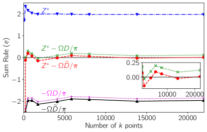
In Fig. 1 we plot the naBEC , standard DW , and modified DW , for FCC Al versus the number of -points used to sample the Brillouin zone of the conventional cubic cell 222Note that the cubic symmetry means and, e.g., .. Since FCC Al has no optical modes, the nonadiabatic regime is hardly relevant here from a physical point of view; yet, its computational simplicity allows for a numerical test of our arguments. Remarkably, the naBEC of Al does not vanish in spite of it being an elemental metal, and converges to a value of around 2. We see from the red dashed curve that the sum rule in Eq. (6) is accurately satisfied for a large enough mesh. We also see that differs slightly from , and this results in a violation of the naBEC sum rule that is modest ( ) but clearly discerned for the numerical accuracy of our calculations. We find a similar qualitative behavior for all materials in this study (see, e.g., SM SM Figs. S9-S11); thus, we shall exclusively focus on henceforth.
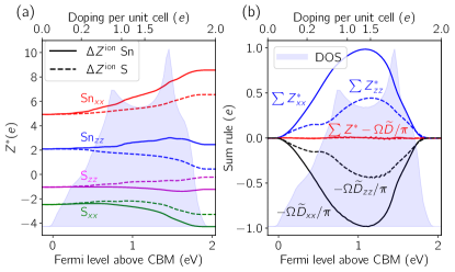
We now consider bulk SnS2, a layered insulator that has shown considerable promise for use in a wide range of device applications Seo et al. (2008); Luo et al. (2012); Song et al. (2013a, b); Yu et al. (2014); Chu et al. (2018) We dope SnS2 with electrons into the isolated, lowest-energy Sn()-S() conduction band (see Fig. S2(b) in the SM SM ). In order to accurately describe the Fermi surface, we perform the Brillouin-zone integrals of Eqs. (7) and (8) via Wannier interpolation to a dense mesh (see SM SM Secs. S2 B).
In Fig. 2(a), we show the naBECs versus doping for the Sn and S sublattices, in the in-plane and out-of-plane directions. The dotted curves in Fig. 2(a) correspond to the excess ionic charge placed on the S sublattices, and the solid curves to the charge placed on the Sn sublattice. In Fig. 2(b) we see that the violation of the (sublattice-summed) BEC charge neutrality condition increases as we dope to roughly half of the conduction-band width, and then decreases back to zero when the conduction band is filled. The DW exhibits the same behavior, and we see from the red curves around zero, that the naBEC sum rule [Eq. (6)] is accurately satisfied.
Finally we calculate the naBECs and DW for the electron-doped cubic phase of STO, which has attracted significant attention due to its superconducting properties Schooley et al. (1965); Huang and Hoffman (2017); Collignon et al. (2019). To illustrate the behavior of the naBECs, we present doping across the entire Ti conduction band manifold (see Fig. S2(a) SM ), even though it is not expected to be experimentally achievable. (Also, we should note that significant changes to the electronic and atomic structure are expected if such calculations at high doping are performed with atomic relaxations Bjaalie et al. (2014).)
In Fig. 3(a)-(c) we plot the naBECs for the sublatticies in STO with doping. The oxygens are labelled as “equatorial” (on faces parallel to for BEC element ) and “apical” (on faces perpendicular to ). Different trends in result from different choices of sublattice for chemical doping, suggesting significant qualitative changes in frequencies of polar-phonon modes depending on the sublattice that is doped versus the sublattice(s) involved in the phonon displacements. Fig. 3(a) corresponds to doping on the Sr site, e.g., by La substitution; in this case, the Sr increases significantly to compensate the decrease of the Ti , resulting from the fact that the electrons are doped into the Ti orbitals;this effect is significantly reduced if we consider doping on the Ti site in panel (b) (e.g., by Nb substitution). For doping on the O site (e.g., by the formation of O vacancies), the decrease in the Ti is now partially compensated by the increase in for the O sublattices.
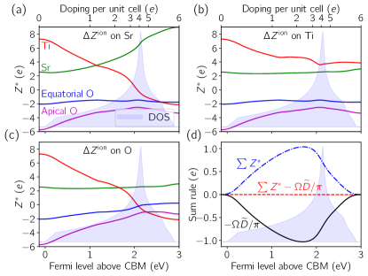
In Fig. 3(d), we see very similar behavior to Fig. 2(b), i.e., the sublattice sum of the BECs increasingly deviates from zero with doping towards the middle of the conduction-band manifold, and then decreases. As with SnS2, the naBEC sum rule is accurately satisfied.
In conclusion, we have demonstrated that nonadiabatic Born effective charges are well defined in metals with time-reversal symmetry, and generalized the acoustic sum rule to the full nonadiabatic regime, where the sublattice sum of the nonadiabatic Born effective charges equals the Drude weight. The rigorous understanding and first-principles description of nonadiabatic Born effective charges provided by this work opens up several future directions for study. For example, it will allow quantitative predictions of plasmon-phonon coupling, and the implications for transport in doped semiconductor devices such as transparent conductors. Direct comparison with experimental probes such as infrared or Raman scattering will serve to validate the theory and aid in materials characterization. It may also shed light on the physics of ferroelectric metals, possibly providing additional tools to quantify the amplitude of the polar lattice distortion.
Acknowledgements.
We thank D. Vanderbilt and R. Resta for discussions and insightful comments on the manuscript. CED acknowledges support from the National Science Foundation under Grant No. DMR-1918455. SC acknowledges support from the National Science Foundation under Grant No. DMR-1848074. MS acknowledges support from the European Research Council (ERC) through Grant “MULTIFLEXO” No. 724529; from Ministerio de Economia, Industria y Competitividad (MINECO-Spain) through Grants No. PID2019-108573GB-C22 and No. CEX2019-000917-S; and from Generalitat de Catalunya (Grant No. 2017 SGR1506). The Flatiron Institute is a division of the Simons Foundation.References
- Born and Huang (1954) M. Born and K. Huang, Dynamical theory of crystal lattices (Clarendon press, 1954).
- Lyddane et al. (1941) R. H. Lyddane, R. G. Sachs, and E. Teller, Phys. Rev. 59, 673 (1941).
- Pick et al. (1970) R. M. Pick, M. H. Cohen, and R. M. Martin, Phys. Rev. B 1, 910 (1970).
- Gonze and Lee (1997) X. Gonze and C. Lee, Phys. Rev. B 55, 10355 (1997).
- Vogl (1976) P. Vogl, Phys. Rev. B 13, 694 (1976).
- Sjakste et al. (2015) J. Sjakste, N. Vast, M. Calandra, and F. Mauri, Phys. Rev. B 92, 054307 (2015).
- Verdi and Giustino (2015) C. Verdi and F. Giustino, Phys. Rev. Lett. 115, 176401 (2015).
- Martin (1972) R. M. Martin, Phys. Rev. B 5, 1607 (1972).
- Hong and Vanderbilt (2013) J. Hong and D. Vanderbilt, Phys. Rev. B 88, 174107 (2013).
- Stengel (2013a) M. Stengel, Phys. Rev. B 88, 174106 (2013a).
- Resta et al. (1993) R. Resta, M. Posternak, and A. Baldereschi, Phys. Rev. Lett. 70, 1010 (1993).
- Zhong et al. (1994) W. Zhong, R. D. King-Smith, and D. Vanderbilt, Phys. Rev. Lett. 72, 3618 (1994).
- Ghosez et al. (1998) P. Ghosez, J.-P. Michenaud, and X. Gonze, Phys. Rev. B 58, 6224 (1998).
- Resta (1994) R. Resta, Rev. Mod. Phys. 66, 899 (1994).
- Anderson and Blount (1965) P. W. Anderson and E. Blount, Phys. Rev. Lett. 14, 217 (1965).
- Shi et al. (2013) Y. Shi, Y. Guo, X. Wang, A. J. Princep, D. Khalyavin, P. Manuel, Y. Michiue, A. Sato, K. Tsuda, S. Yu, et al., Nat. Mater. 12, 1024 (2013).
- Born and Oppenheimer (1927) M. Born and R. Oppenheimer, Annalen der Physik 389, 457 (1927).
- Petretto et al. (2018) G. Petretto, S. Dwaraknath, H. P.C. Miranda, D. Winston, M. Giantomassi, M. J. van Setten, X. Gonze, K. A. Persson, G. Hautier, and G.-M. Rignanese, Scientific Data 5, 180065 (2018).
- Varga (1965) B. B. Varga, Phys. Rev. 137, A1896 (1965).
- Olson and Lynch (1969) C. G. Olson and D. W. Lynch, Phys. Rev. 177, 1231 (1969).
- Calandra et al. (2010) M. Calandra, G. Profeta, and F. Mauri, Phys. Rev. B 82, 165111 (2010).
- Engelsberg and Schrieffer (1963) S. Engelsberg and J. R. Schrieffer, Phys. Rev. 131, 993 (1963).
- Maksimov and Shulga (1996) E. Maksimov and S. Shulga, Solid State Commun. 97, 553 (1996).
- Saitta et al. (2008) A. M. Saitta, M. Lazzeri, M. Calandra, and F. Mauri, Phys. Rev. Lett. 100, 1 (2008).
- Pisana et al. (2007) S. Pisana, M. Lazzeri, C. Casiraghi, K. S. Novoselov, A. K. Geim, A. C. Ferrari, and F. Mauri, Nat. Mater. 6, 198 (2007).
- Bistoni et al. (2019) O. Bistoni, P. Barone, E. Cappelluti, L. Benfatto, and F. Mauri, 2D Materials 6, 045015 (2019).
- Binci et al. (2021) L. Binci, P. Barone, and F. Mauri, Phys. Rev. B 103, 134304 (2021).
- Baroni et al. (2001) S. Baroni, S. de Gironcoli, A. Dal Corso, and P. Giannozzi, Rev. Mod. Phys. 73, 515 (2001).
- Giustino (2017) F. Giustino, Rev. Mod. Phys. 89, 015003 (2017).
- Adler (1962) S. L. Adler, Phys. Rev. 126, 413 (1962).
- Allen (1993) P. B. Allen, in Conceptual Foundations of Materials: A Standard Model for Ground- and Excited-State Properties, edited by S. G. Louie and M. L. Cohen (Elsevier B.V., Amsterdam, The Netherlands, 1993) Chap. 6, pp. 165–218.
- Resta (2018) R. Resta, J. Phys. Condens. Mat. 30, aade19 (2018).
- Note (1) The negative sign compared to Eq. (1) reflects the fact that the time derivative of the vector potential is minus the electric field, .
- Thouless et al. (1982) D. J. Thouless, M. Kohmoto, M. P. Nightingale, and M. den Nijs, Phys. Rev. Lett. 49, 405 (1982).
- Gonze (1997) X. Gonze, Phys. Rev. B 55, 10337 (1997).
- Stengel (2013b) M. Stengel, Nat. Commun. 4, 2693 (2013b), article.
- Stengel and Vanderbilt (2018) M. Stengel and D. Vanderbilt, Phys. Rev. B 98, 125133 (2018).
- Schiaffino et al. (2019) A. Schiaffino, C. E. Dreyer, D. Vanderbilt, and M. Stengel, Phys. Rev. B 99, 085107 (2019).
- Kohn and Sham (1965) W. Kohn and L. J. Sham, Phys. Rev. 140, A1133 (1965).
- (40) See supplemental material [URL to be inserted by publisher] for details of the DFPT formalism, computational approach and convergence, and details about treatment of the doping, which includes Refs. Perdew and Wang, 1992; Gonze et al., 2009; Hamann, 2013; Perdew et al., 1996; Mostofi et al., 2014; Ge and Lu, 2015; Lihm and Park, 2021; Lu et al., 2012 .
- van Leeuwen (2004) R. van Leeuwen, Phys. Rev. B 69, 115110 (2004).
- Ismail-Beigi et al. (2001) S. Ismail-Beigi, E. K. Chang, and S. G. Louie, Phys. Rev. Lett. 87, 087402 (2001).
- Pickard and Mauri (2003) C. J. Pickard and F. Mauri, Phys. Rev. Lett. 91, 196401 (2003).
- Dreyer et al. (2018) C. E. Dreyer, M. Stengel, and D. Vanderbilt, Phys. Rev. B 98, 075153 (2018).
- Note (2) Note that the cubic symmetry means and, e.g., .
- Seo et al. (2008) J.-w. Seo, J.-t. Jang, S.-w. Park, C. Kim, B. Park, and J. Cheon, Adv. Mater. 20, 4269 (2008).
- Luo et al. (2012) B. Luo, Y. Fang, B. Wang, J. Zhou, H. Song, and L. Zhi, Energy & Environmental Science 5, 5226 (2012).
- Song et al. (2013a) H. Song, S. Li, L. Gao, Y. Xu, K. Ueno, J. Tang, Y. Cheng, and K. Tsukagoshi, Nanoscale 5, 9666 (2013a).
- Song et al. (2013b) H. Song, S. Li, L. Gao, Y. Xu, K. Ueno, J. Tang, Y. Cheng, and K. Tsukagoshi, Nanoscale 5, 9666 (2013b).
- Yu et al. (2014) J. Yu, C.-Y. Xu, F.-X. Ma, S.-P. Hu, Y.-W. Zhang, and L. Zhen, ACS Appl. Mater. Inter. 6, 22370 (2014).
- Chu et al. (2018) W. Chu, X. Li, S. Li, J. Hou, Q. Jiang, and J. Yang, ACS Appl. Energy Mater. 2, 382 (2018).
- Schooley et al. (1965) J. F. Schooley, W. R. Hosler, E. Ambler, J. H. Becker, M. L. Cohen, and C. S. Koonce, Phys. Rev. Lett. 14, 305 (1965).
- Huang and Hoffman (2017) D. Huang and J. E. Hoffman, Annu. Rev. Condens. Matt. Phys. 8, 311 (2017).
- Collignon et al. (2019) C. Collignon, X. Lin, C. W. Rischau, B. Fauqué, and K. Behnia, Annu. Rev. Condens. Matt. Phys. 10, 25 (2019).
- Bjaalie et al. (2014) L. Bjaalie, A. Janotti, B. Himmetoglu, and C. G. Van de Walle, Phys. Rev. B 90, 195117 (2014).
- Perdew and Wang (1992) J. P. Perdew and Y. Wang, Phys. Rev. B 45, 13244 (1992).
- Gonze et al. (2009) X. Gonze, B. Amadon, P.-M. Anglade, J.-M. Beuken, F. Bottin, P. Boulanger, F. Bruneval, D. Caliste, R. Caracas, M. Côté, T. Deutsch, L. Genovese, P. Ghosez, M. Giantomassi, S. Goedecker, D. Hamann, P. Hermet, F. Jollet, G. Jomard, S. Leroux, M. Mancini, S. Mazevet, M. Oliveira, G. Onida, Y. Pouillon, T. Rangel, G.-M. Rignanese, D. Sangalli, R. Shaltaf, M. Torrent, M. Verstraete, G. Zerah, and J. Zwanziger, Computer Physics Communications 180, 2582 (2009).
- Hamann (2013) D. R. Hamann, Phys. Rev. B 88, 085117 (2013).
- Perdew et al. (1996) J. P. Perdew, K. Burke, and M. Ernzerhof, Phys. Rev. Lett. 77, 3865 (1996).
- Mostofi et al. (2014) A. A. Mostofi, J. R. Yates, G. Pizzi, Y.-S. Lee, I. Souza, D. Vanderbilt, and N. Marzari, Computer Physics Communications 185, 2309 (2014).
- Ge and Lu (2015) X. Ge and D. Lu, Phys. Rev. B 92, 241107 (2015).
- Lihm and Park (2021) J.-M. Lihm and C.-H. Park, Phys. Rev. X 11, 041053 (2021).
- Lu et al. (2012) H. Lu, C.-W. Bark, D. Esque de los Ojos, J. Alcala, C. B. Eom, G. Catalan, and A. Gruverman, Science 336, 59 (2012).