centres in photonic silicon-on-insulator material
Abstract
Global quantum networks will benefit from the reliable creation and control of high-performance solid-state telecom photon-spin interfaces. T radiation damage centres in silicon provide a promising photon-spin interface due to their narrow -band optical transition near nm and long-lived electron and nuclear spin lifetimes. To date, these defect centres have only been studied as ensembles in bulk silicon. Here, we demonstrate the reliable creation of high concentration T centre ensembles in the 220 nm device layer of silicon-on-insulator (SOI) wafers by ion implantation and subsequent annealing. We then develop a method that uses spin-dependent optical transitions to benchmark the characteristic optical spectral diffusion within these T centre ensembles. Using this new technique, we show that with minimal optimization to the fabrication process high densities of implanted T centres localized nm from an interface display GHz characteristic levels of total spectral diffusion.
I Introduction
Point defect colour centres in solid state systems provide a promising platform for emerging quantum technologies. A number of colour centres are currently in development Awschalom et al. (2018); Zhang et al. (2020), but few of these leading candidates are both natively integrated into silicon and intrinsically operate at telecom wavelengths. Radiation damage centres in silicon have recently emerged as promising light-matter interfaces that simultaneously meet both of these criteria Buckley et al. (2017); Chartrand et al. (2018); Beaufils et al. (2018); Redjem et al. (2020). Within this family of defects, the T centre notably possesses highly coherent electron and nuclear spin degrees of freedom and narrow, spin-dependent ensemble optical transitions near nm in the telecommunications -band Bergeron et al. (2020). These properties make the T centre a competitive candidate for integration into future commercial-scale quantum networks with long-lived quantum memory and computing capabilities.
Incorporating T centres into such quantum networks requires a reliable means of making the centres in device-ready material such as silicon-on-insulator (SOI). Other photon-spin interfaces have been produced by ion implantation and thermal treatment Meijer et al. (2005); Chu et al. (2014); Falk et al. (2013); Beaufils et al. (2018); Phenicie et al. (2019); Buckley et al. (2020); Redjem et al. (2020). Here, we use similar techniques to generate high concentrations of T centres in the 220nm device layer of commercial SOI wafers. We achieve T centre concentrations times higher than in previously measured bulk samples and, in follow-on work kur , present evidence that these SOI concentrations are cm-3. Moreover, the inhomogeneous broadening of the zero phonon line (ZPL) within implanted ensembles is only larger than in T centre ensembles generated by electron irradiating and annealing comparable bulk material.
The fabrication process used to generate T centres should preserve the excellent spin and optical properties that T centre ensembles exhibit in bulk silicon where the majority of centres are located far from material interfaces. The increase in electric and magnetic field noise near those interfaces can dramatically degrade a centre’s spin and optical properties. Encouragingly, donor spin defects in silicon have already demonstrated competitive electron and nuclear spin coherence times ( s, s) at distances of just nm from /SiO2 interfaces Muhonen et al. (2014), and T centres can be expected to demonstrate comparable or better spin properties at our target depth of nm. In the optical domain, spectral diffusion — the time-varying changes in a centre’s optical transition energies — often dominates the optical properties of emitters located near interfaces. Spectral diffusion can reduce the indistinguishability of emitted photons, limiting an emitter’s potential in quantum technologies. Measuring the characteristic spectral diffusion of the generated T centre ensembles thus provides an important metric for benchmarking our fabrication process. To this end, we develop a method that uses spin-dependent optical transitions to efficiently measure the characteristic long-term (total) spectral diffusion within an ensemble of emitters.
Applying this new technique to our high-concentration T centre ensembles in SOI, we measure characteristic total spectral diffusion of GHz. Although this value is times larger than the kHz lifetime-limited linewidth, excellent photon indistinguishability could still be achieved by employing fabrication or measurement techniques designed to stabilize the electromagnetic environment de Oliveira et al. (2017); Anderson et al. (2019); Sangtawesin et al. (2019); Kasperczyk et al. (2020), by filtering the emitted photons Bernien et al. (2013); Guo et al. (2019), or by Purcell-enhancing the radiative decay rate Grange et al. (2015); Giesz et al. (2015) as the T centre is expected to have a high radiative efficiency Bergeron et al. (2020).
II T Centre Implantation
As shown in Fig. 1a, the T centre is thought to consist of two carbon atoms sharing the substitutional site of one silicon atom; an interstitial hydrogen terminates one of these carbon atoms while the other remains stable with an unpaired electron Safonov et al. (1996). The current formation model for this defect consists of an interstitial carbon capturing a hydrogen atom and then migrating to a substitutional carbon site during heat treatment at temperatures between and C Safonov et al. (1996); Bergeron et al. (2020). Starting from SOI with a nm thick Czochralski (CZ) natural Si (Si) device layer and µm of buried SiO2, we realize this formation process by implanting carbon and then hydrogen in a fixed [C:H]=1:1 dose ratio, annealing between the two implants and then again after the hydrogen implant.
We performed two fabrication runs: one with a 12C implant and doses of cm-2 and a second with 13C and doses of cm-2. These doses, which were chosen from measurements detailed in the Supplementary Materials (SM) SI , place the initial carbon concentrations well above the carbon solubility limit for silicon at C Pichler (2004). Carbon implants were performed at an energy of keV, while hydrogen was implanted at keV to target overlapping implantation profiles with a mean depth of nm.
In between the two implants, we perform a rapid thermal anneal at C for seconds in an argon background to repair lattice damage generated during the carbon implant and to incorporate carbon onto substitutional lattice sites Berhanuddin et al. (2012); Beaufils et al. (2018). The subsequent hydrogen implant then generates lattice damage and interstitial carbon to promote T centre formation, but the smaller mass of the hydrogen ions generates less total damage than the carbon implant SI . After the hydrogen implant, we boil the samples for hour in deionized water to further increase the hydrogen concentration before performing a final rapid thermal anneal for min at a temperature ranging from to C in a nitrogen atmosphere.
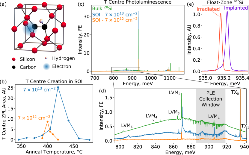
Fig. 1b shows the integrated area of the T centre ZPL as a function of the final anneal temperature for a series of SOI samples. For these samples, we find optimum temperatures of C for a fluence of cm-2 and C for cm-2. Unless otherwise noted, we have normalized photoluminescence (PL) spectra to the free exciton (FE) recombination line at meV. Although the FE recombination line can vary in intensity across samples as, for instance, the density of recombination sites changes, it provides a means of roughly quantifying the T centre concentration to enable comparison amongst samples.
In Fig. 1c,d, we plot the PL spectra under above-band ( nm) excitation for these particular SOI samples alongside that of an isotopically-purified 28Si bulk sample with an initial cm-3 carbon concentration. T centres were created in this bulk sample by electron irradiating and annealing (details in Ref. Bergeron et al. (2020)). Fig. 1d provides a detailed view of the T centre sideband spectra, showing an isotopic shift in the local vibrational modes (LVMs) as the cm-2 SOI sample was implanted with 13C isotopes, the cm-2 SOI sample was implanted with 12C, and the bulk 28Si sample contains a natural distribution of carbon isotopes ( 12C). In Fig. 1d, we have also labeled both ZPLs within the T centre exciton doublet, where sits meV above Bergeron et al. (2020).
By normalizing the integrated area of the T centre ZPL to the nominal sample thickness, we estimate that the implanted T centre densities for the cm-2 and cm-2 SOI samples are and times larger than the T centre density in the bulk 28Si sample, respectively. Here, we have used nm as the SOI thickness and the µm absorption depth of nm light in silicon at cryogenic temperatures Dash and Newman (1955); Jellison Jr. and Joshi (2018) as the nominal 28Si thickness. As the free excitons generated by the nm excitation are not confined to the absorption region in our bulk sample, this latter thickness serves as a lower bound, making our relative concentration estimates lower bounds on the true ratios. In the SM, we verify that the implanted T centres are localized to the SOI device layer by selectively etching away the device layer and also by using ultraviolet PL excitation, which has a much shallower absorption depth than nm SI . We also note that this estimate of the T centre density neglects differences in the defects’ local optical environment that could modify their emission properties Barnes (1998).
In Fig. 1e, we compare the ZPL PL for T centres generated by implantation to that of T centres created by electron irradiation. Both samples in this figure are bulk, float-zone (FZ) Si. One was implanted with 13C and hydrogen at a fluence of cm-2, while the other was electron irradiated and annealed to convert native carbon and hydrogen into T centres Bergeron et al. (2020). We once again see the expected 13C isotopic shift in the implanted ZPL, and at K, we report ZPL linewidths of GHz in the irradiated FZ sample and GHz for the implanted FZ wafer. As will be shown below, these linewidths lie well above the linewidth of our 28Si sample and below that of our CZ SOI samples. Among these measurements, however, this comparison between FZ Si samples provides the best comparison between implanted and irradiated linewidths as each used similar material outside the “semiconductor vacuum” of 28Si Saeedi et al. (2013). We thus report only a increase in the inhomogeneous broadening for our implanted ensembles compared to ensembles generated by electron irradiation, and we expect that the broader lines we observe in CZ SOI will be reduced for T centres created by implantation into a FZ SOI device layer.
III Hyperpolarization
In other solid state emitters that lack inversion symmetry, spectral diffusion has been shown to increase when centres are generated by ion implantation van Dam et al. (2019); Kasperczyk et al. (2020) or as centres approach interfaces due to a dramatic increase in electric and magnetic field noise in these regions Ishikawa et al. (2012); Evans et al. (2016); Crook et al. (2020). Typically, spectral diffusion is measured by tracking spectral lines of individual emitters. Here, we develop a novel technique for measuring spectral diffusion within an ensemble of emitters and use it to compare the optical properties of the T centres in our SOI samples to those in bulk samples.
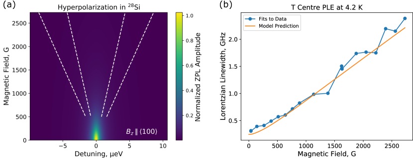
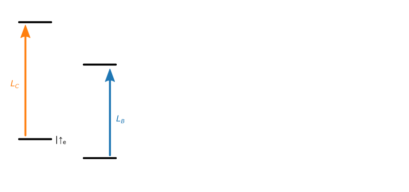
Under spin-selective resonant optical driving, the T centre ground state electron spin will hyperpolarize through a process shown schematically in Fig. 2a. This unpaired electron provides a spin degree of freedom with an isotropic -factor of in the orbital ground state. Upon resonant generation of a bound exciton (BE), the ground state electron pairs with the BE electron to form a spin- singlet. The BE hole then provides an unpaired spin with an anisotropic -factor in the BE state. A magnetic field thus generates a spin splitting () in the ground (excited, or ) state where is the Bohr magneton. Because these splittings can differ in magnitude, for Zeeman splittings larger than the homogeneous optical linewidth, only one spin sublevel will be excited by the resonant optical drive. Spin non-conserving relaxation will then shelve the system in whichever state is not addressed by the optical drive, hyperpolarizing the electron spin as the T centre is optically cycled. For the T centre, this hyperpolarization mechanism is efficient Bergeron et al. (2020).
Using this process, we can reveal the characteristic homogeneous optical linewidth of an ensemble by measuring how the resonantly-driven ZPL evolves in a magnetic field. In the absence of any homogeneous broadening effects, an individual T centre’s optical linewidth will approach its lifetime-limited lower bound and observable hyperpolarization at low magnetic fields is expected. This onset of hyperpolarization only weakly depends on the inhomogeneously-broadened ensemble lineshape and will apply to ensembles in 28Si and Si alike. Homogeneous effects such as thermal broadening or spectral diffusion will delay this onset of hyperpolarization to larger magnetic fields as shown schematically in Fig. 2b. If these homogeneous mechanisms have a characteristic broadening on the same scale as the spin splitting, they will ensure that each spin sublevel is intermittently addressed by the optical field, reducing the level of hyperpolarization in the system and increasing the measured PL.
In Fig. 2c, we perform PLE spectroscopy of the T centre ZPL in the bulk 28Si sample by scanning a tunable laser over the optical resonance and measuring the PL emission within the collection window highlighted in Fig. 1d. Repeating this measurement as a function of , we see that, rather than Zeeman splitting along the dashed lines of Fig. 2c, the PLE trace remains stationary and slowly decays as the interrogated T centres hyperpolarize. This measurement was performed at a temperature of K where the ZPL linewidth is thermally-broadened Bergeron et al. (2020) and with aligned along the crystal axis. For this field orientation, we expect the hole -factors for the twelve possible T centre orientational subsets relative to to take on the values with multiplicities of and , respectively Safonov et al. (1995); SI .
The measured hyperpolarization dynamics can be modeled by noting that both spin sublevels must be driven to prevent population shelving. With a magnetic field applied, the spin sublevels split by where each sublevel is assumed to have the same optical homogeneous linewidth . As the spin states separate and the probability of driving both sublevels decreases, the system starts to hyperpolarize. Assuming weak optical driving, we model this process with a rate model using the levels and transitions shown schematically in Fig. 2d and find that the amplitude of a partially hyperpolarized PLE spectrum (Fig. 2e) is proportional to
| (1) |
where is the Lorentzian amplitude of the spin-down (spin-up) sublevel and is the optical detuning from the zero-field resonance. For simplicity, we have neglected optical transitions between states with different spin orientations, which have smaller spectral overlap with other transitions and have been shown for T centres to be much weaker than optical transitions between spin states of the same orientation Bergeron et al. (2020). The effect of these transitions is examined in the SM SI .
Evaluating Eq. 1 and normalizing to the , value, we obtain an expression for the PLE amplitude as a function of magnetic field for a single T centre:
| (2) |
Because we simultaneously interrogate a large number of T centres in twelve possible orientational subsets, we model our measurement by averaging Eq. 2 across the twelve values of . Here, we have assumed that each orientation contributes equally to the measured signal.
Fitting the data in Fig. 2c to this model, we extract a homogeneous linewidth of MHz, which agrees very well with the purely thermal linewidth of MHz at K calculated from the thermal broadening data in Ref. Bergeron et al. (2020) as well as the MHz linewidth obtained by fitting the PLE spectrum in the G residual magnetic field of our setup. These fits are shown in the insets to Fig. 2c, and the SM provides additional plots demonstrating good agreement between the modeled and measured data SI . The large uncertainty in is dominated by uncertainties in sample alignment and -factor calculations as detailed in the SM SI . Simultaneous magnetic resonance measurements in a magnetic field could address these sources of uncertainty by providing in situ calibration of the -factors for an arbitrary sample orientation.
IV Spectral Diffusion in Bulk Si
When cooled to K, the thermal broadening contribution to the ZPL linewidth is kHz, and the ZPL PLE linewidth in the 28Si sample narrows to MHz SI . In the absence of significant thermal broadening, we may assume that measuring amounts to measuring the total spectral diffusion linewidth . To measure at K, we resonantly drive the T centre ZPL and ramp . Fitting the normalized data shown in Fig. 3a to Eq. 2 averaged over the twelve orientational subsets, we find MHz for our bulk 28Si sample which agrees with the measured . We stress this model only considers homogeneous broadening and ignores any inhomogeneities that might be present. For our measurements of , we integrate PL counts for s at each value of , making this a long-term average value of the characteristic spectral diffusion within the T centre ensemble.
To demonstrate that this method can provide a means of measuring ensemble homogeneous linewidths that are not resolved in an inhomogeneously broadened PLE spectrum, we repeat this measurement on T centres in our bulk FZ Si sample, which has an inhomogeneously-broadened optical linewidth of GHz at K. To include this inhomogeneous broadening in our hyperpolarization model, we replace in Eq. 2 to account for inhomogeneously-shifted resonances and convolve the result with a distribution of described by a Gauss-Lorentz product with a full width at half maximum equal to the measured optical linewidth . For simplicity, we restrict ourselves to , and once again, we model contributions from different T centre orientational subsets by averaging the calculated response over the expected distribution of .
Because our single crystal Si sample has been cut along an unknown crystallographic axis, we can only extract an upper bound on by fitting the measured data shown in Fig. 3b as a function of magnetic field alignment and selecting the orientation that maximizes as detailed in the SM SI . From this maximal orientation, we find MHz (the orange curve in Fig. 3b). For comparison, we then assume the measured decay is entirely dictated by inhomogeneous broadening and plot the behaviour predicted by Eq. 2 with equal to the inhomogeneous linewidth GHz. The resulting model curve (shown in green in Fig. 3b) fails to match the data. As these models are calculated for bounding cases, we can comfortably conclude that this method extracts linewidths narrower than .
V Spectral Diffusion in SOI
Lastly, we use this method to benchmark the optical properties of implanted T centres in CZ SOI. At K, the SOI samples shown in Fig. 1d display inhomogeneously-broadened ZPL linewidths of GHz and GHz for the samples implanted with fluences of cm-2 and cm-2, respectively. We measure the PLE amplitude as a function of over the range of for which our optical setup remains stable, and we find GHz and GHz, respectively. Notably, the sample that received the lower implant fluence shows a slightly reduced level of spectral diffusion. This suggests that at least some portion of could be attributable to our fabrication process and might be improved with additional surface treatment Sangtawesin et al. (2019), reduced implant fluence van Dam et al. (2019); Wolfowicz et al. (2020), or further processing.

It is important to note that the assumption of equally weighted contributions from each T centre orientation is likely not true. To address this, we have also fit our data under the assumption that the measured signal comes entirely from the T centre orientation that minimizes (maximizes) to obtain the bounding sets GHz and GHz for the cm-2 and cm-2 samples, respectively. Once again, simultaneous magnetic resonance measurements in a magnetic field could improve the precision of this technique by calibrating the relative signal contributions of different orientations.
Even with this uncertainty, however, this method provides efficient comparative measurements of and rapid feedback on fabrication processes designed to reduce . Measuring PLE decay due to spin-dependent optical transitions can provide the characteristic within an ensemble of emitters when complementary techniques such as spectral hole burning Völker (1989) are not possible. Moreover, because our measurements interrogate a large ensemble of T centres simultaneously, the technique developed here enables quick access to the characteristic value of across a sample, which can be time consuming to obtain by measuring individual centres.
VI Outlook
Although far from the lifetime-limited linewidth of kHz Bergeron et al. (2020) and times larger than the values we report in bulk samples, these values for of implanted T centres in CZ SOI are already competitive with other solid state emitters near interfaces. It is common for spectral diffusion in defect centres that lack inversion symmetry to be on the order of several GHz in the absence of careful surface treatment or experimental protocols Ishikawa et al. (2012); Evans et al. (2016); Anderson et al. (2019); van Dam et al. (2019); Crook et al. (2020). With minimal optimization, implanted T centres display GHz characteristic spectral diffusion, and this could be minimized further as fabrication and measurement techniques continue to develop. Moreover, the characteristic spectral diffusion reported here is a long-term, ensemble average. Individual centres within this ensemble could have much lower Chu et al. (2014); Kasperczyk et al. (2020), and any slowly varying effects that contribute to this long-term average might be addressed by feedback or filtering techniques Bernien et al. (2013); Guo et al. (2019).
To estimate the effect spectral diffusion will have on the performance of a T centre-based photon-spin interface, we calculate the indistinguishability of two photons emitted by a given T centre as where is the T centre Debye-Waller factor Bylander et al. (2003); Grange et al. (2015); Bergeron et al. (2020). For our bulk and SOI samples, respectively, we find and . We stress that both of these values can likely be improved by employing fabrication or measurement techniques designed to stabilize the electromagnetic environment de Oliveira et al. (2017); Anderson et al. (2019); Sangtawesin et al. (2019); Kasperczyk et al. (2020) or by filtering the emitted photons Bernien et al. (2013); Guo et al. (2019). Moreover, embedding T centres inside optical resonators can Purcell enhance to increase the photon indistinguishabilty. Optical resonators in SOI capable of demonstrating Purcell factors above have already been demonstrated Zain et al. (2008). Because the T centre radiative efficiency is expected to be near-unity Bergeron et al. (2020), T centres incorporated into such an optical cavity could provide high quality photon-spin interfaces in the telecommunications -band.
In summary, we have demonstrated a reliable method for using ion implantation and annealing treatments to incorporate T centres into industry-standard silicon integrated photonics material. We then developed an efficient method, which could be applied to a wide variety of colour centres, for using spin-dependent optical transitions to benchmark spectral diffusion. Finally, we used this new technique to show that implanted T centres within a nm SOI device layer can display GHz-scale levels of spectral diffusion with minimal optimization. These results represent an important step towards developing quantum technologies in silicon.
VII Acknowledgments
We thank M. L. W. Thewalt and L. Childress for fruitful discussions as well as N. V. Abrosimov for bulk sample growth and C. Clément for rapid thermal annealing.
VIII Funding
This work was supported by the Natural Sciences and Engineering Research Council of Canada (NSERC), the Canada Research Chairs program (CRC), the Canada Foundation for Innovation (CFI), the B.C. Knowledge Development Fund (BCKDF), the Canadian Institute for Advanced Research (CIFAR) Quantum Information Science program, the CIFAR Catalyst Fund, and Le Fonds de recherche du Québec – Nature et technologies (FRQNT). The 28Si samples used in this study were prepared from the Avo28 crystal produced by the International Avogadro Coordination (IAC) Project (2004–2011) in cooperation among the BIPM, the INRIM (Italy), the IRMM (EU), the NMIA (Australia), the NMIJ (Japan), the NPL (UK), and the PTB (Germany).
IX References
References
- Awschalom et al. (2018) D. D. Awschalom, R. Hanson, J. Wrachtrup, and B. B. Zhou, Nature Photonics 12, 516 (2018).
- Zhang et al. (2020) G. Zhang, Y. Cheng, J.-P. Chou, and A. Gali, Applied Physics Reviews 7, 031308 (2020).
- Buckley et al. (2017) S. Buckley, J. Chiles, A. N. McCaughan, G. Moody, K. L. Silverman, M. J. Stevens, R. P. Mirin, S. W. Nam, and J. M. Shainline, Applied Physics Letters 111, 141101 (2017).
- Chartrand et al. (2018) C. Chartrand, L. Bergeron, K. J. Morse, H. Riemann, N. V. Abrosimov, P. Becker, H.-J. Pohl, S. Simmons, and M. L. W. Thewalt, Phys. Rev. B 98, 195201 (2018).
- Beaufils et al. (2018) C. Beaufils, W. Redjem, E. Rousseau, V. Jacques, A. Y. Kuznetsov, C. Raynaud, C. Voisin, A. Benali, T. Herzig, S. Pezzagna, et al., Phys. Rev. B 97, 035303 (2018).
- Redjem et al. (2020) W. Redjem, A. Durand, T. Herzig, A. Benali, S. Pezzagna, J. Meijer, A. Y. Kuznetsov, H. S. Nguyen, S. Cueff, J. M. Gérard, et al., Nat. Electron. 3, 738 (2020).
- Bergeron et al. (2020) L. Bergeron, C. Chartrand, A. T. K. Kurkjian, K. J. Morse, H. Riemann, N. V. Abrosimov, P. Becker, H.-J. Pohl, M. L. W. Thewalt, and S. Simmons, PRX Quantum 1, 020301 (2020).
- Meijer et al. (2005) J. Meijer, B. Burchard, M. Domhan, C. Wittmann, T. Gaebel, I. Popa, F. Jelezko, and J. Wrachtrup, Applied Physics Letters 87, 261909 (2005).
- Chu et al. (2014) Y. Chu, N. de Leon, B. Shields, B. Hausmann, R. Evans, E. Togan, M. J. Burek, M. Markham, A. Stacey, A. Zibrov, et al., Nano Letters 14, 1982 (2014).
- Falk et al. (2013) A. L. Falk, B. B. Buckley, G. Calusine, W. F. Koehl, V. V. Bobrovitski, A. Politi, C. A. Zorman, P. X.-L. Feng, and D. D. Awschalom, Nat. Commun. 4, 1819 (2013).
- Phenicie et al. (2019) C. M. Phenicie, P. Stevenson, S. Welinski, B. C. Rose, A. T. Asfaw, R. J. Cava, S. A. Lyon, N. P. de Leon, and J. D. Thompson, Nano Letters 19, 8928 (2019).
- Buckley et al. (2020) S. M. Buckley, A. N. Tait, G. Moody, B. Primavera, S. Olson, J. Herman, K. L. Silverman, S. P. Rao, S. W. Nam, R. P. Mirin, et al., Opt. Express 28, 16057 (2020).
- (13) A. T. K. Kurkjian, D. B. Higginbottom, et al, in preparation.
- Muhonen et al. (2014) J. T. Muhonen, J. P. Dehollain, A. L. ans Fay E. Hudson, R. Kalra, T. Sekiguchi, K. M. Itoh, D. N. Jamieson, J. C. McCallum, A. S. Dzurak, and A. Morello, Nature Nanotech. 9, 986 (2014).
- de Oliveira et al. (2017) F. F. de Oliveira, D. Antonov, Y. Wang, P. Neumann, S. A. Momenzadeh, T. Häußermann, A. Pasquarelli, A. Denisenko, and J. Wrachtrup, Nat Commun 8, 15409 (2017).
- Anderson et al. (2019) C. P. Anderson, A. Bourassa, K. C. Miao, G. Wolfowicz, P. J. Mintun, A. L. Crook, H. Abe, J. Ul Hassan, N. T. Son, T. Ohshima, et al., Science 366, 1225 (2019).
- Sangtawesin et al. (2019) S. Sangtawesin, B. L. Dwyer, S. Srinivasan, J. J. Allred, L. V. H. Rodgers, K. De Greve, A. Stacey, N. Dontschuk, K. M. O’Donnell, D. Hu, et al., Phys. Rev. X 9, 031052 (2019).
- Kasperczyk et al. (2020) M. Kasperczyk, J. A. Zuber, A. Barfuss, J. Kölbl, V. Yurgens, S. Flågan, T. Jakubczyk, B. Shields, R. J. Warburton, and P. Maletinsky, Phys. Rev. B 102, 075312 (2020), URL https://link.aps.org/doi/10.1103/PhysRevB.102.075312.
- Bernien et al. (2013) H. Bernien, B. Hensen, W. Pfaff, G. Koolstra, M. S. Blok, L. Robledo, T. H. Taminiau, M. Markham, D. J. Twitchen, L. Childress, et al., Nature 497, 86 (2013).
- Guo et al. (2019) K. Guo, H. Springbett, T. Zhu, R. A. Oliver, Y. Arakawa, and M. J. Holmes, Appl. Phys. Lett. 114, 112109 (2019).
- Grange et al. (2015) T. Grange, G. Hornecker, D. Hunger, J.-P. Poizat, J.-M. Gérard, P. Senellart, and A. Auffèves, Phys. Rev. Lett. 114, 193601 (2015).
- Giesz et al. (2015) V. Giesz, S. L. Portalupi, T. Grange, C. Antón, L. De Santis, J. Demory, N. Somaschi, I. Sagnes, A. Lemaître, L. Lanco, et al., Phys. Rev. B 92, 161302 (2015), URL https://link.aps.org/doi/10.1103/PhysRevB.92.161302.
- Safonov et al. (1996) A. N. Safonov, E. C. Lightowlers, G. Davies, P. Leary, R. Jones, and S. Öberg, Phys. Rev. Lett. 77, 4812 (1996).
- (24) See Supplementary Information.
- Pichler (2004) P. Pichler, Isovalent Impurities (Springer Vienna, Vienna, 2004), pp. 281–329, ISBN 978-3-7091-0597-9.
- Berhanuddin et al. (2012) D. D. Berhanuddin, M. A. Lournco, R. M. Gwilliam, and K. P. Homewood, Adv. Funct. Mater. 22, 2709 (2012).
- Dash and Newman (1955) W. C. Dash and R. Newman, Phys. Rev. 99, 1151 (1955).
- Jellison Jr. and Joshi (2018) G. E. Jellison Jr. and P. C. Joshi, Spectroscopic Ellipsometry for Photovoltaics (Springer, 2018), vol. 1, chap. 8.
- Barnes (1998) W. L. Barnes, Journal of Modern Optics 45, 661 (1998).
- Saeedi et al. (2013) K. Saeedi, S. Simmons, J. Z. Salvail, P. Dluhy, H. Riemann, N. V. Abrosimov, P. Becker, H.-J. Pohl, J. J. L. Morton, and M. L. W. Thewalt, Science 342, 830 (2013).
- van Dam et al. (2019) S. B. van Dam, M. Walsh, M. J. Degen, E. Bersin, S. L. Mouradian, A. Galiullin, M. Ruf, M. IJspeert, T. H. Taminiau, R. Hanson, et al., Phys. Rev. B 99, 161203 (2019).
- Ishikawa et al. (2012) T. Ishikawa, K.-M. C. Fu, C. Santori, V. M. Acosta, R. G. Beausoleil, K. Watanabe, S. Chikata, and K. M. Itoh, Nano Lett. 12, 2083 (2012).
- Evans et al. (2016) R. E. Evans, A. Sipahigil, D. D. Sukachev, A. S. Zibrov, and M. D. Lukin, Phys. Rev. Applied 5, 044010 (2016).
- Crook et al. (2020) A. L. Crook, C. P. Anderson, K. C. Miao, A. Bourassa, H. Lee, S. L. Bayliss, D. O. Bracher, X. Zhang, H. Abe, T. Ohshima, et al., Nano Letters 20, 3427 (2020).
- Safonov et al. (1995) A. N. Safonov, E. C. Lightowlers, and G. Davies, Materials Science Forum 196-201, 909 (1995).
- Wolfowicz et al. (2020) G. Wolfowicz, F. J. Heremans, C. P. Anderson, S. Kanai, H. Seo, A. Gali, G. Galli, and D. D. Awschalom, arXiv:2010.16395 (2020).
- Völker (1989) S. Völker, Annu. Rev. Phys. Chem. 40, 499 (1989).
- Bylander et al. (2003) J. Bylander, I. Robert-Philip, and I. Abram, Eur. Phys. J. D 22, 295 (2003).
- Zain et al. (2008) A. R. M. Zain, N. P. Johnson, M. Sorel, and R. M. D. L. Rue, Opt. Express 16, 12084 (2008).
X Supplementary Information
X.1 Measurement Details
The samples are mounted in a liquid helium cryostat. The sample temperature is set by pumping on the liquid helium bath. The PL and PLE spectroscopy measurements were performed as reported in Ref. Bergeron et al. (2020). For PLE spectroscopy measurements a Toptica DL100 tunable diode laser was used for measurements of 28Si, and a tunable nanoplus DFB laser diode was used for the broader SOI and bulk Si samples.
X.2 Implantation Dose Optimization
To select an implant dose for our T centre implantation study, we first generated T centres in float zone (FZ) silicon wafers by co-implanting carbon and hydrogen. We swept the fluence of the implants while keeping fixed C:H ratios of 1:1, 2:1, and 1:0. Carbon implants were again performed at an energy of keV, and hydrogen was implanted at keV. The samples were then annealed in air following a C step-wise temperature profile with dwell times of min. This temperature profile was chosen as it previously generated high density T centre concentrations in electron-irradiated, high-carbon bulk samples.
Fig. 5a shows the integrated area of the FE-normalized T centre ZPL for each fluence we measured, and Fig. 5b presents the PL spectra for the implant fluences that generated the brightest T centre ZPL for each C:H ratio. Each spectrum shows a strong T centre ZPL, but the 1:0 C:H sample has a much higher broadband radiation damage background. By comparison, the 1:1 and 2:1 C:H implants show comparable T centre intensity with a much lower background for carbon fluences of cm-2. From this data, we decided to fix the C:H ratio at 1:1 and implant at fluences of cm-2 and cm-2.
X.3 T Centre Localization
To confirm the generated T centres are localized within the SOI device layer, we etched away the device layer from one of our SOI samples and measured PL from the exposed buried oxide and handle wafer material. As shown in Fig. 6a, the resulting nm PL spectrum shows no significant T centre PL as compared to the same sample in an unetched region, suggesting that the handle material does not contain a significant concentration of T centres.
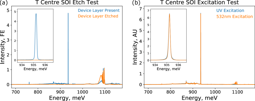
As further confirmation that the generated T centres are localized within the SOI device layer, we performed PL spectroscopy with UV excitation. Because the absorption depth of nm light in Si is µm at cryogenic temperatures, the SOI PL spectra presented in the main text sample both the SOI device layer and the silicon handle wafer beneath the buried oxide. UV wavelengths have a penetration depth of µm in Si at cryogenic temperatures Dash and Newman (1955); Jellison Jr. and Joshi (2018), making PL with UV excitation more sensitive to the device layer than PL with nm excitation. Fig. 6b shows a representative PL spectrum measured on the same sample with both nm excitation and UV excitation. Because the UV measurement shows a negligible FE recombination line, we have normalized both spectra to their integrated signal. Both spectra show strong T centre lines, confirming that there are T centres within the device layer.
Taken together, these two measurements localize our implanted T centres to within the device layer of the SOI materal.
X.4 Calculating g-factors
Our calculation of the hole -factors expands upon the work of Ref. Safonov et al. (1995). We write the hole Hamiltonian as the sum of a strain and a magnetic term where the strain Hamiltonian is
| (3) |
Here, are the angular momentum operators, , are strain tensor components, and , are deformation parameters. An external magnetic field enters the Hamiltonian as
| (4) |
where is the Bohr magneton and , are the hole -factors.
We use the internal strain and deformation parameters obtained by Ref. Safonov et al. (1995): , , eV, and eV. The internal strain parameters were defined relative to the defect axes where is parallel to and is in the plane, tilted from the axis by . In our treatment, we rotate the internal strain from the defect coordinate system to that of the crystal so that magnetic field alignments can be referenced to crystallographic axes.
Rather than using the and values from Ref. Safonov et al. (1995), we obtain and by fitting the model above to the -factors obtained in Ref. Bergeron et al. (2020), restricting ourselves to values near those reported in Ref. Safonov et al. (1995). The highly-resolved 28Si data from Ref. Bergeron et al. (2020) enables us to fit the hole -factors using all twelve T centre orientational subsets. For this fit, we also introduce a misalignment of the magnetic field as an additional free parameter. Our fit returns an angular inclination of and rotation of about the nominal field alignment in that work. Table 1 provides comparisons between our fit results and the values reported in Ref. Bergeron et al. (2020) for a magnetic field alignment.
| Subset | Measured Bergeron et al. (2020) | Fitted | Calculated |
|---|---|---|---|
| 1 | |||
| 2 | |||
| 3 | |||
| 4 | |||
| 5 | |||
| 6 | |||
| 7 | |||
| 8 | |||
| 9 | |||
| 10 | |||
| 11 | |||
| 12 |
With model parameters in hand, we then calculate for each T centre orientational subset by finding the components for each subset, computing the eigenvalues of , and dividing the resulting spin splitting by . predicts a negligible zero-field splitting within the orbital branch and negligible interaction with the orbital at the moderate magnetic fields used in this work, justifying this approach for calculating the values.
The -factors for used in the main text are listed with their calculated error bars in Table 1. For these calculations, we have assigned inclination and azimuthal -field alignment errors of each.
For our bounding calculation of in , we fit the measured data as a function of the magnetic field alignment. The fitted values for are plotted as a function of the magnetic field orientation in Fig. 7. Here, we have omitted magnetic field orientations for which the model is unable to fit the measured data. The model curve in Fig. 3b of the main text is plotted using inclination and azimuthal angles of and , respectively.
X.5 Optical Transitions Between Different Spin Orientations
In the model presented in the main text, we have neglected optical transitions between different spin orientations. Including these transitions into the rate model used to derive Eq. 1 of the main text, we can rewrite the amplitude proportionality as
| (5) |
where the optical transitions are labeled by subscripts as in Fig. 8a. The amplitudes , have been measured to be times larger than , Bergeron et al. (2020); kur . Moveover, since , the approximation given by Eq. 1 of the main text becomes better as increases.
To quantify the effect of the and optical transitions on our hyperpolarization model, we fit the thermally-broadened K data displayed in Fig. 2c of the main text using the four-transition model of Eq. 5. Ignoring inhomogeneous broadening, we find MHz with and MHz with . To further explore this dependency, we fix , fit the measured data as a function of , and compare the homogeneous linewidth extracted from the model to the optically measured linewidth MHz. Plotting the results in Fig. 8b, we see that only becomes strongly dependent on when , as expected. In this regime, the hyperpolarization model returns values of that are much larger than the optically-measured value, supporting the assertion that that has been experimentally verified elsewhere Bergeron et al. (2020); kur .
X.6 Fitting residual-field PLE spectra
The poles of the electromagnet used in these measurements generated a residual field of G. For our 28Si sample, the Zeeman splitting from this residual field is comparable to the measured optical linewidth . To account for this in our analysis, we fit the residual field spectra to an ensemble average of Eq. 2 with along the axis and take .
For the Si and SOI samples where the lineshape is better described by the Gauss-Lorentz product (GLP), we define the GLP linewidth to be .
X.7 Hyperpolarization model linecuts
In Fig. 2c of the main text, we measure T centre hyperpolarization in our 28Si sample at K and compare the measured data to the behaviour predicted by the hyperpolarization model developed in the text. As additional comparison, we plot the simulated 2d data in Fig. 9a. We then fit both the measured and the modeled PLE spectra to Lorentzian lineshapes and plot the fitted linewidths against each other in Fig. 9b.