Rapid microwave-only characterization and readout of quantum dots using multiplexed gigahertz-frequency resonators
Abstract
Superconducting resonators enable fast characterization and readout of mesoscopic quantum devices. Finding ways to perform measurements of interest on such devices using resonators only is therefore of great practical relevance. We report the experimental investigation of an InAs nanowire multi-quantum dot device by probing GHz resonators connected to the device. First, we demonstrate accurate extraction of the DC conductance from measurements of the high-frequency admittance. Because our technique does not rely on DC calibration, it could potentially obviate the need for DC measurements in semiconductor qubit devices. Second, we demonstrate multiplexed gate sensing and the detection of charge tunneling on microsecond time scales. The GHz detection of dispersive resonator shifts allows rapid acquisition of charge-stability diagrams, as well as resolving charge tunneling in the device with a signal-to-noise ratio of up to 15 in one microsecond. Our measurements show that GHz-frequency resonators may serve as a universal tool for fast tune-up and high-fidelity readout of semiconductor qubits.
I Introduction
Microwave resonators in the few-GHz range are well-known as a powerful means to increase the speed with which properties of mesoscopic quantum devices can be read out [1]. In the field of quantum information, resonators in this so called ‘Super High Frequency’ (SHF) band have thus enabled the fast and high-fidelity non-demolition readout of quantum bits (qubits)[2, 3, 4, 5], as well as mediating interactions between qubits [6, 7, 8, 9]. SHF resonators are also an attractive tool for the fast characterization of quantum devices, because the required tune-up routines are generally time-consuming. Additionally, frequency multiplexing using many high-Q resonators has been established for hardware-efficient mass-characterization of devices [10, 11].
Efficient characterization is particularly relevant for semiconductor quantum devices where many gate electrodes result in a large parameter space. In recent years there have been numerous efforts to utilize SHF resonators for this purpose [12, 13, 14, 15] as well as reading out qubit degrees of freedom [16, 17, 18, 19, 20, 21, 22, 23, 24, 25, 26]. Despite these successes, however, experiments are still often supplemented with DC or low-frequency measurements to quantitatively extract the DC conductance [27]. As larger-scale devices are developed [28, 29], it is interesting to direct focus to readout and tune-up schemes utilizing SHF resonators only, thus allowing a single framework for all measurements performed on a device.
Here, we present experiments using multiplexed resonators in the 3–7 GHz range coupled to a multi-quantum dot (QD) system. Using the resonator response only we are able to infer quantitatively the DC conductance of the system, and detect single-electron tunneling with high signal-to-noise ratio (SNR) on sub-microsecond timescales. The remainder of this paper is organized as follows: In Sec. III we determine the DC (i.e., zero-frequency) conductance from SHF measurements without any DC calibration data and find agreement with conductance obtained from a DC transport control measurement. In Sec. IV, we demonstrate fast multiplexed dispersive gate sensing (DGS) at -frequencies in a double quantum dot (DQD). This local measurement of charge transitions facilitates fast tune-up of multi-QD systems [29]. Finally, in Sec. V, we attain high SNRs in the detection of charge tunneling in the DQD. State-dependent charge-tunneling is a key mechanism for qubit readout in semiconductor qubits [30]. Our optimized resonator design [31], combined with the use of a near-quantum limited amplifier [32], results in a maximum SNR of 15 in one microsecond integration time.
II Experimental setup
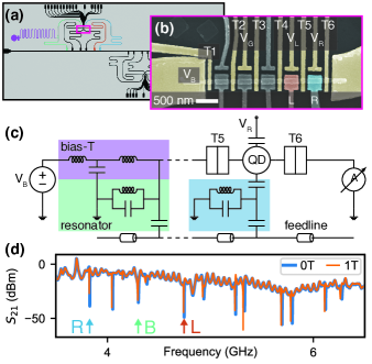
The device comprises an InAs nanowire with a GHz-bandwidth coplanar waveguide (CPW) resonator [33] coupled to every QD to sense the electronic compressibility of each individual dot. An additional resonator that is galvanically connected to the source of the nanowire is used to probe the admittance of the nanowire. Fig. 1a and b show images of the resonators and the multi-QD device respectively. An approximate lumped-element schematic of the device is shown in Fig. 1c. Each resonator is coupled to a central feedline in a hanger geometry and is individually addressable using frequency multiplexing (Fig. 1d). The obtained SNR is set by the high resonator bandwidth, optimized resonator coupling quality factors, and a traveling wave parametric amplifier (TWPA) [32] at the base temperature stage of of our dilution refrigerator. For further details see the supplemental material.
III High frequency conductance measurements
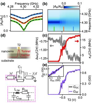
We begin by investigating the SHF response of the resonator coupled to the lead in response to changing nanowire conductance [34, 12, 13, 27, 35]. Changing the conductance by tuning the gate voltage T2 modulates the resonator response, shown in Fig. 2a and b, through changes in its load admittance. The DC conductance can be extracted from the load admittance either by building up a calibration map of load admittance and DC conductance, or by quantitatively modeling the resonator circuit [27]. We take the latter approach to maintain independence from DC calibration measurements. To quantify the modulation of the resonator response, we fit the response to a hanger input-output model [36, 37, 38]. The relevant parameters for extracting load admittance are the change in the resonance frequency and the additional photon decay rate with respect to the pinched-off regime, which is reached by decreasing the gate voltages until saturates. Representative fits are plotted in Fig. 2a and the extracted and are shown in Fig. 2c. The load admittance, , can then be calculated by
| (1) |
which holds for a transmission line resonator of characteristic impedance coupled to a high impedance load . We estimate from the resonator design. See the supplemental material for more details on the procedure outlined above.
Importantly, the load admittance at finite frequency does not directly translate to the DC conductance of the coupled device (i.e., the nanowire). The nanowire itself has an inductive component and the gates surrounding the nanowire add additional shunting capacitive paths to ground, contributing to the load admittance especially for higher frequencies. Our device design with high lever-arm gates necessitates compensating for these contributions explicitly, in contrast to the experiments in Refs. [12, 13, 27]. To account for these effects, we model the load admittance as in Fig. 2d, describing an effective transmission line formed by the nanowire split by a tunnel junction. We denote the series resistance, inductance and parallel capacitance per unit length of this transmission line by and and introduce with the nanowire length. DC conductance of the nanowire can be calculated from the impedance added by the nanowire itself, , and the impedance of the tunnel junction .
The relation between and depends on the fractional position of the tunnel junction along the nanowire, which we parameterize by . Explicitly, the relation is given by
| (2) |
where denotes the complex propagation constant.
The constants and are determined from two SHF calibration measurements. For the first calibration measurement, the load impedance is measured when all gates are open at , corresponding to the limit that . For the second calibration measurement, the load impedance as and is measured by pinching off the rightmost gate T6. Solving the resulting two equations for and yields
| (3) |
See supplemental material for more information. Using Eq. (2) and Eq. (3), we then extract from the admittance . We model the junction as a resistor and capacitor in parallel such that [39], and then determine the DC-equivalent conductance as
| (4) |
To validate our method to infer the conductance, we compare it to the conductance obtained from a control experiment using conventional DC-current detection. Fig. 2e shows the conductance extracted from DC measurements and the DC conductance extracted from the resonator response . Excellent agreement is observed between and for data from pinch-off traces of T1 through T6, changing according to the position of the gate, shown in the inset of Fig. 2e.
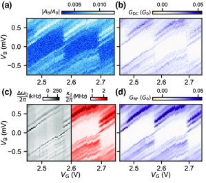
Applications of RF conductance are not limited to measuring the impedance of tunnel gates [40, 41, 15, 42]. As an example, we probe a quantum dot by tuning T2 and T3 into the tunneling regime. We show the amplitude response of the lead resonator on resonance in Fig. 3a as a function of bias voltage and gate voltage . Even though the amplitude response is not translated into DC conductance here, it shows all the qualitative features present in the control data measured by DC lock-in conductance (Fig. 3b), including the excited states of the quantum dot. The amplitude response of Fig. 3a is part of a full frequency trace, measured to also allow for a quantitative comparison between the DC results and the resonator response. From these traces, the frequency shift and photon decay are extracted and shown in Fig. 3c. We use the model defined by Eqs. (1 - 4) to obtain , shown in Fig. 3d. This is the same model used for the tunnel junction scans of Fig. 2. Note that we neglect here the finite width occupied by the quantum dot and its internal structure; nevertheless we observe reasonable agreement between and .
IV Rapid multiplexed reflectometry

We now move on to the capacitively coupled gate resonators and investigate DGS in the double quantum dot (DQD) regime [43, 17, 44, 45, 46, 47, 48, 49, 25, 50, 51, 52]. To tune the system into a DQD, the voltages of gates T4, T5, and T6 are each decreased into the tunneling regime. Accordingly, two quantum dots are formed under the rightmost two topgates in the nanowire[39].
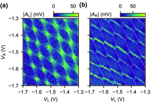
A resonator is coupled to both dots to sense the electronic compressibility of the individual dots [53, 54]. In Fig. 4 we show a charge stability diagram (CSD) using and to change the electron occupation of the DQD. We perform pulsed readout with an integration time of per point, constituting a total data acquisition time of for the entire CSD [14, 55]. The data acquisition is frequency-multiplexed for both resonators such that the data in panels a and b of Fig. 4 are measured simultaneously [56, 29]. This not only reduces the measurement time, but multiplexing also guarantees the measurements in Fig. 4a and b correspond to the exact same physical regime, regardless of charge jumps and gate hysteresis. To emphasize the correspondence between Fig. 4a and b, the same guides to the eye outlining stable charge configurations are drawn on both figures.
Resonators are only sensitive to charge transitions involving the quantum dots they are coupled to. Therefore, both resonators show the interdot transitions, but only the left/right resonator is sensitive to transitions to the left/right lead respectively. Hence multiplexing also enables spatial correlation of electron tunneling by comparing the DGS signal from each gate’s resonator, effectively ‘tracking’ the electron through the device.
V Signal to noise
Finally, we investigate the attainable SNR for resolving charge tunneling with DGS by changing detuning from charge degeneracy in the DQD. This procedure serves as a proxy for different qubit states in schemes where readout is based on state-dependent tunneling [57, 58, 50, 35, 25, 59]. Because actual qubit systems will have limitations on the readout power [30] we investigate the SNR at both a fixed ‘low’ excitation voltage in the resonator, , as well as at an optimized excitation voltage, . These excitation voltages are calculated from the generator power and line attenuation in addition to the resonator frequency and coupling capacitance to the feedline.
We fix the total charge in the system by pinching off gates on either side of the DQD. The only remaining transitions are interdot transitions occurring through a tunnel coupling denoted by . The resonator response as a function of the energy detuning from the interdot transition, is shown in Fig. 5a. We determine by fitting the resonator response to an input-output model [18], discussed in the supplemental material. Linecuts of the fit results and measurement data are shown in Fig. 5b.
We define SNR as the change in signal between charge degeneracy and Coulomb blockade divided by the noise. To measure it, we perform a series of pulsed measurements of I and Q with a pulse time of at both Coulomb blockade and charge degeneracy, and show the obtained histograms for an integration time of in Fig. 5c. These histograms are fit with a Gaussian to extract the separation between the Gaussian peaks in the IQ plane as well as their average standard deviation representing the width. The SNR is given by .
In Fig. 5d we plot the dependence of SNR on , which approaches a square root dependence for longer times. We attribute the discrepancy between attained SNR and a square root dependence for pulse times shorter than to the finite bandwidth of the resonators. For these pulse lengths, the resonator cannot reach a steady state photon population, limiting the signal available for readout.
Next, we compare the observed SNR with expected theoretical limits. The change in signal at the feedline level — with the gain of the amplification chain in the system — can never exceed the total voltage swing in the feedline . The fit to the data in Fig. 5a, used to extract , also provides a direct measurement of the ratio , close to the absolute maximum. In other words, the resonator is coupled near-optimally for this tunnel coupling, such that its external coupling rate is nearly equal to the dispersive shift.
The achievable SNR together is then set by together with noise temperature, , and readout time, , as:
| (5) |
where is the impedance of the feedline, see supplemental material. The found in Fig. 5c together with the readout time, and the deduced approximate voltage swing in the feedline, corresponds to a noise temperature estimate of . To improve the SNR, one can either increase the readout time or readout power, as shown in Fig. 5d. In practice, limits to these two parameters will be determined by the specific qubit implementation. Specifically, by optimizing the excitation voltage and tunnel coupling together, an of is achieved at .
VI Conclusions
We have shown the characterization of an InAs nanowire multi-QD system using -frequency sensing. Probing the finite frequency admittance of the nanowire has allowed us to infer the low-frequency conductance with good accuracy, even without calibration from DC measurements. Further, we have shown high-SNR dispersive sensing on timescales near the bandwidth limit set by the Q factor of the resonators. Besides their use for qubit devices, we envision that fast multiplexed readout of quantum devices may be used for more complex sensing schemes. In particular, rapid simultaneous conduction of multiple local measurements could facilitate unique quantum transport experiments because they provide spatial information about tunneling processes. For example, probing two quantum dots at either end of a central charge island, tunneling events into the outer dots may be correlated [60, 61]. We conclude that multiplexed SHF resonators may serve as a complete toolset for characterization and readout of semiconductor quantum devices, and present intriguing opportunities for developing novel and high-speed quantum transport measurement schemes.
VII Acknowledgements
We thank D. Bouman and J.D. Mensingh for nanowire deposition and A. Bargerbos for valuable comments on the manuscript. We further thank N.P. Alberts, O.W.B. Benningshof, R.N. Schouten, M.J.Tiggelman, and R.F.L. Vermeulen for valuable technical assistance. This work has been supported by the Netherlands Organization for Scientific Research (NWO) and Microsoft.
References
- Schoelkopf et al. [1998] R. J. Schoelkopf, P. Wahlgren, A. A. Kozhevnikov, P. Delsing, and D. E. Prober, The radio-frequency single-electron transistor (rf-set): A fast and ultrasensitive electrometer, Science 280, 1238 (1998).
- Blais et al. [2004] A. Blais, R.-S. Huang, A. Wallraff, S. M. Girvin, and R. J. Schoelkopf, Cavity quantum electrodynamics for superconducting electrical circuits: An architecture for quantum computation, Physical Review A 69, 062320 (2004).
- Wallraff et al. [2005] A. Wallraff, D. I. Schuster, A. Blais, L. Frunzio, J. Majer, M. H. Devoret, S. M. Girvin, and R. J. Schoelkopf, Approaching unit visibility for control of a superconducting qubit with dispersive readout, Physical Review Letters 95, 060501 (2005).
- Vijay et al. [2011] R. Vijay, D. H. Slichter, and I. Siddiqi, Observation of quantum jumps in a superconducting artificial atom, Physical Review Letters 106, 110502 (2011).
- Walter et al. [2017] T. Walter, P. Kurpiers, S. Gasparinetti, P. Magnard, A. Potočnik, Y. Salathé, M. Pechal, M. Mondal, M. Oppliger, C. Eichler, and A. Wallraff, Rapid high-fidelity single-shot dispersive readout of superconducting qubits, Physical Review Applied 7, 054020 (2017).
- Majer et al. [2007] J. Majer, J. M. Chow, J. M. Gambetta, J. Koch, B. R. Johnson, J. A. Schreier, L. Frunzio, D. I. Schuster, A. A. Houck, A. Wallraff, A. Blais, M. H. Devoret, S. M. Girvin, and R. J. Schoelkopf, Coupling superconducting qubits via a cavity bus, Nature 449, 443 (2007).
- Sillanpää et al. [2007] M. A. Sillanpää, J. I. Park, and R. W. Simmonds, Coherent quantum state storage and transfer between two phase qubits via a resonant cavity, Nature 449, 438 (2007).
- Scarlino et al. [2019] P. Scarlino, D. J. van Woerkom, U. C. Mendes, J. V. Koski, A. J. Landig, C. K. Andersen, S. Gasparinetti, C. Reichl, W. Wegscheider, K. Ensslin, T. Ihn, A. Blais, and A. Wallraff, Coherent microwave-photon-mediated coupling between a semiconductor and a superconducting qubit, Nature Communications 10, 3011 (2019).
- Borjans et al. [2019] F. Borjans, X. G. Croot, X. Mi, M. J. Gullans, and J. R. Petta, Resonant microwave-mediated interactions between distant electron spins, Nature 577, 195 (2019).
- Jerger et al. [2012] M. Jerger, S. Poletto, P. Macha, U. Hübner, E. Il’ichev, and A. V. Ustinov, Frequency division multiplexing readout and simultaneous manipulation of an array of flux qubits, Applied Physics Letters 101, 042604 (2012).
- Jeffrey et al. [2014] E. Jeffrey, D. Sank, J. Mutus, T. White, J. Kelly, R. Barends, Y. Chen, Z. Chen, B. Chiaro, A. Dunsworth, A. Megrant, P. O’Malley, C. Neill, P. Roushan, A. Vainsencher, J. Wenner, A. Cleland, and J. M. Martinis, Fast accurate state measurement with superconducting qubits, Physical Review Letters 112, 190504 (2014).
- Puebla-Hellmann and Wallraff [2012] G. Puebla-Hellmann and A. Wallraff, Realization of gigahertz-frequency impedance matching circuits for nano-scale devices, Applied Physics Letters 101, 053108 (2012).
- Hasler et al. [2015] T. Hasler, M. Jung, V. Ranjan, G. Puebla-Hellmann, A. Wallraff, and C. Schönenberger, Shot noise of a quantum dot measured with gigahertz impedance matching, Physical Review Applied 4, 054002 (2015).
- Stehlik et al. [2015] J. Stehlik, Y.-Y. Liu, C. Quintana, C. Eichler, T. Hartke, and J. Petta, Fast charge sensing of a cavity-coupled double quantum dot using a josephson parametric amplifier, Physical Review Applied 4, 014018 (2015).
- Ranjan et al. [2015] V. Ranjan, G. Puebla-Hellmann, M. Jung, T. Hasler, A. Nunnenkamp, M. Muoth, C. Hierold, A. Wallraff, and C. Schönenberger, Clean carbon nanotubes coupled to superconducting impedance-matching circuits, Nature Communications 6, 7165 (2015).
- Delbecq et al. [2011] M. R. Delbecq, V. Schmitt, F. D. Parmentier, N. Roch, J. J. Viennot, G. Fève, B. Huard, C. Mora, A. Cottet, and T. Kontos, Coupling a quantum dot, fermionic leads, and a microwave cavity on a chip, Physical Review Letters 107, 256804 (2011).
- Frey et al. [2012] T. Frey, P. J. Leek, M. Beck, A. Blais, T. Ihn, K. Ensslin, and A. Wallraff, Dipole coupling of a double quantum dot to a microwave resonator, Physical Review Letters 108, 046807 (2012).
- Petersson et al. [2012] K. D. Petersson, L. W. McFaul, M. D. Schroer, M. Jung, J. M. Taylor, A. A. Houck, and J. R. Petta, Circuit quantum electrodynamics with a spin qubit, Nature 490, 380 (2012).
- Mi et al. [2016] X. Mi, J. V. Cady, D. M. Zajac, P. W. Deelman, and J. R. Petta, Strong coupling of a single electron in silicon to a microwave photon, Science 355, 156 (2016).
- Stockklauser et al. [2017] A. Stockklauser, P. Scarlino, J. Koski, S. Gasparinetti, C. Andersen, C. Reichl, W. Wegscheider, T. Ihn, K. Ensslin, and A. Wallraff, Strong coupling cavity QED with gate-defined double quantum dots enabled by a high impedance resonator, Physical Review X 7, 011030 (2017).
- Bruhat et al. [2018] L. E. Bruhat, T. Cubaynes, J. J. Viennot, M. C. Dartiailh, M. M. Desjardins, A. Cottet, and T. Kontos, Circuit QED with a quantum-dot charge qubit dressed by cooper pairs, Physical Review B 98, 155313 (2018).
- Landig et al. [2018] A. J. Landig, J. V. Koski, P. Scarlino, U. C. Mendes, A. Blais, C. Reichl, W. Wegscheider, A. Wallraff, K. Ensslin, and T. Ihn, Coherent spin–photon coupling using a resonant exchange qubit, Nature 560, 179 (2018).
- Mi et al. [2018] X. Mi, M. Benito, S. Putz, D. M. Zajac, J. M. Taylor, G. Burkard, and J. R. Petta, A coherent spin–photon interface in silicon, Nature 555, 599 (2018).
- Samkharadze et al. [2018] N. Samkharadze, G. Zheng, N. Kalhor, D. Brousse, A. Sammak, U. C. Mendes, A. Blais, G. Scappucci, and L. M. K. Vandersypen, Strong spin-photon coupling in silicon, Science 359, 1123 (2018).
- Zheng et al. [2019] G. Zheng, N. Samkharadze, M. L. Noordam, N. Kalhor, D. Brousse, A. Sammak, G. Scappucci, and L. M. K. Vandersypen, Rapid gate-based spin read-out in silicon using an on-chip resonator, Nature Nanotechnology 14, 742 (2019).
- Koski et al. [2020] J. V. Koski, A. J. Landig, M. Russ, J. C. Abadillo-Uriel, P. Scarlino, B. Kratochwil, C. Reichl, W. Wegscheider, G. Burkard, M. Friesen, S. N. Coppersmith, A. Wallraff, K. Ensslin, and T. Ihn, Strong photon coupling to the quadrupole moment of an electron in a solid-state qubit, Nature Physics 16, 642 (2020).
- Harabula et al. [2017] M.-C. Harabula, T. Hasler, G. Fülöp, M. Jung, V. Ranjan, and C. Schönenberger, Measuring a quantum dot with an impedance-matching on-chip superconducting LC resonator at gigahertz frequencies, Physical Review Applied 8, 054006 (2017).
- Holman et al. [2020] N. Holman, D. Rosenberg, D. Yost, J. L. Yoder, R. Das, W. D. Oliver, R. McDermott, and M. A. Eriksson, Dispersive measurement of a semiconductor double quantum dot via 3d integration of a high-impedance tin resonator (2020), arXiv:2011.08759 [cond-mat.mes-hall] .
- Ruffino et al. [2021] A. Ruffino, T.-Y. Yang, J. Michniewicz, Y. Peng, E. Charbon, and M. F. Gonzalez-Zalba, Integrated multiplexed microwave readout of silicon quantum dots in a cryogenic cmos chip (2021), arXiv:2101.08295 [quant-ph] .
- Maman et al. [2020] V. D. Maman, M. Gonzalez-Zalba, and A. Pályi, Charge noise and overdrive errors in dispersive readout of charge, spin, and majorana qubits, Physical Review Applied 14, 064024 (2020).
- Ahmed et al. [2018] I. Ahmed, J. A. Haigh, S. Schaal, S. Barraud, Y. Zhu, C. min Lee, M. Amado, J. W. A. Robinson, A. Rossi, J. J. L. Morton, and M. F. Gonzalez-Zalba, Radio-frequency capacitive gate-based sensing, Physical Review Applied 10, 014018 (2018).
- Macklin et al. [2015] C. Macklin, K. O'Brien, D. Hover, M. E. Schwartz, V. Bolkhovsky, X. Zhang, W. D. Oliver, and I. Siddiqi, A near-quantum-limited josephson traveling-wave parametric amplifier, Science 350, 307 (2015).
- Kroll et al. [2019] J. Kroll, F. Borsoi, K. van der Enden, W. Uilhoorn, D. de Jong, M. Quintero-Pérez, D. van Woerkom, A. Bruno, S. Plissard, D. Car, E. Bakkers, M. Cassidy, and L. Kouwenhoven, Magnetic-field-resilient superconducting coplanar-waveguide resonators for hybrid circuit quantum electrodynamics experiments, Physical Review Applied 11, 064053 (2019).
- Chorley et al. [2012] S. J. Chorley, J. Wabnig, Z. V. Penfold-Fitch, K. D. Petersson, J. Frake, C. G. Smith, and M. R. Buitelaar, Measuring the complex admittance of a carbon nanotube double quantum dot, Physical Review Letters 108, 036802 (2012).
- Razmadze et al. [2019] D. Razmadze, D. Sabonis, F. K. Malinowski, G. C. Ménard, S. Pauka, H. Nguyen, D. M. van Zanten, E. C. OFarrell, J. Suter, P. Krogstrup, F. Kuemmeth, and C. M. Marcus, Radio-frequency methods for majorana-based quantum devices: Fast charge sensing and phase-diagram mapping, Physical Review Applied 11, 064011 (2019).
- Khalil et al. [2012] M. S. Khalil, M. J. A. Stoutimore, F. C. Wellstood, and K. D. Osborn, An analysis method for asymmetric resonator transmission applied to superconducting devices, Journal of Applied Physics 111, 054510 (2012).
- Probst et al. [2015] S. Probst, F. B. Song, P. A. Bushev, A. V. Ustinov, and M. Weides, Efficient and robust analysis of complex scattering data under noise in microwave resonators, Review of Scientific Instruments 86, 024706 (2015).
- Guan et al. [2020] H. Guan, M. Dai, Q. He, J. Hu, P. Ouyang, Y. Wang, L. F. Wei, and J. Gao, Network modeling of non-ideal superconducting resonator circuits, Superconductor Science and Technology 33, 075004 (2020).
- van der Wiel et al. [2002] W. G. van der Wiel, S. D. Franceschi, J. M. Elzerman, T. Fujisawa, S. Tarucha, and L. P. Kouwenhoven, Electron transport through double quantum dots, Reviews of Modern Physics 75, 1 (2002).
- Gabelli et al. [2006] J. Gabelli, G. Fève, J.-M. Berroir, B. Plaçais, A. Cavanna, B. Etienne, Y. Jin, and D. C. Glattli, Violation of kirchhoff’s laws for a coherent rc circuit, Science 313, 499 (2006).
- Jung et al. [2012] M. Jung, M. D. Schroer, K. D. Petersson, and J. R. Petta, Radio frequency charge sensing in InAs nanowire double quantum dots, Applied Physics Letters 100, 253508 (2012).
- Ares et al. [2016] N. Ares, F. Schupp, A. Mavalankar, G. Rogers, J. Griffiths, G. Jones, I. Farrer, D. Ritchie, C. Smith, A. Cottet, G. Briggs, and E. Laird, Sensitive radio-frequency measurements of a quantum dot by tuning to perfect impedance matching, Physical Review Applied 5, 034011 (2016).
- Petersson et al. [2010] K. D. Petersson, C. G. Smith, D. Anderson, P. Atkinson, G. A. C. Jones, and D. A. Ritchie, Charge and spin state readout of a double quantum dot coupled to a resonator, Nano Letters 10, 2789 (2010).
- Colless et al. [2013] J. I. Colless, A. C. Mahoney, J. M. Hornibrook, A. C. Doherty, H. Lu, A. C. Gossard, and D. J. Reilly, Dispersive readout of a few-electron double quantum dot with fast rf gate sensors, Physical Review Letters 110, 046805 (2013).
- Betz et al. [2015] A. C. Betz, R. Wacquez, M. Vinet, X. Jehl, A. L. Saraiva, M. Sanquer, A. J. Ferguson, and M. F. Gonzalez-Zalba, Dispersively detected pauli spin-blockade in a silicon nanowire field-effect transistor, Nano Letters 15, 4622 (2015).
- Esmail et al. [2017] A. A. Esmail, A. J. Ferguson, and N. J. Lambert, Cooper pair tunnelling and quasiparticle poisoning in a galvanically isolated superconducting double dot, Applied Physics Letters 111, 252602 (2017).
- Pakkiam et al. [2018] P. Pakkiam, A. Timofeev, M. House, M. Hogg, T. Kobayashi, M. Koch, S. Rogge, and M. Simmons, Single-shot single-gate rf spin readout in silicon, Physical Review X 8, 041032 (2018).
- Urdampilleta et al. [2019] M. Urdampilleta, D. J. Niegemann, E. Chanrion, B. Jadot, C. Spence, P.-A. Mortemousque, C. Bäuerle, L. Hutin, B. Bertrand, S. Barraud, R. Maurand, M. Sanquer, X. Jehl, S. D. Franceschi, M. Vinet, and T. Meunier, Gate-based high fidelity spin readout in a CMOS device, Nature Nanotechnology 14, 737 (2019).
- West et al. [2019] A. West, B. Hensen, A. Jouan, T. Tanttu, C.-H. Yang, A. Rossi, M. F. Gonzalez-Zalba, F. Hudson, A. Morello, D. J. Reilly, and A. S. Dzurak, Gate-based single-shot readout of spins in silicon, Nature Nanotechnology 14, 437 (2019).
- de Jong et al. [2019] D. de Jong, J. van Veen, L. Binci, A. Singh, P. Krogstrup, L. P. Kouwenhoven, W. Pfaff, and J. D. Watson, Rapid detection of coherent tunneling in an InAs nanowire quantum dot through dispersive gate sensing, Physical Review Applied 11, 044061 (2019).
- Sabonis et al. [2019] D. Sabonis, E. C. T. O'Farrell, D. Razmadze, D. M. T. van Zanten, J. Suter, P. Krogstrup, and C. M. Marcus, Dispersive sensing in hybrid InAs/al nanowires, Applied Physics Letters 115, 102601 (2019).
- Crippa et al. [2019] A. Crippa, R. Ezzouch, A. Aprá, A. Amisse, R. Laviéville, L. Hutin, B. Bertrand, M. Vinet, M. Urdampilleta, T. Meunier, M. Sanquer, X. Jehl, R. Maurand, and S. D. Franceschi, Gate-reflectometry dispersive readout and coherent control of a spin qubit in silicon, Nature Communications 10, 2776 (2019).
- Esterli et al. [2019] M. Esterli, R. M. Otxoa, and M. F. Gonzalez-Zalba, Small-signal equivalent circuit for double quantum dots at low-frequencies, Applied Physics Letters 114, 253505 (2019).
- Park et al. [2020] S. Park, C. Metzger, L. Tosi, M. Goffman, C. Urbina, H. Pothier, and A. L. Yeyati, From adiabatic to dispersive readout of quantum circuits, Physical Review Letters 125, 077701 (2020).
- Schupp et al. [2020] F. J. Schupp, F. Vigneau, Y. Wen, A. Mavalankar, J. Griffiths, G. A. C. Jones, I. Farrer, D. A. Ritchie, C. G. Smith, L. C. Camenzind, L. Yu, D. M. Zumbühl, G. A. D. Briggs, N. Ares, and E. A. Laird, Sensitive radiofrequency readout of quantum dots using an ultra-low-noise SQUID amplifier, Journal of Applied Physics 127, 244503 (2020).
- Hornibrook et al. [2014] J. M. Hornibrook, J. I. Colless, A. C. Mahoney, X. G. Croot, S. Blanvillain, H. Lu, A. C. Gossard, and D. J. Reilly, Frequency multiplexing for readout of spin qubits, Applied Physics Letters 104, 103108 (2014).
- Plugge et al. [2017] S. Plugge, A. Rasmussen, R. Egger, and K. Flensberg, Majorana box qubits, New Journal of Physics 19, 012001 (2017).
- Karzig et al. [2017] T. Karzig, C. Knapp, R. M. Lutchyn, P. Bonderson, M. B. Hastings, C. Nayak, J. Alicea, K. Flensberg, S. Plugge, Y. Oreg, C. M. Marcus, and M. H. Freedman, Scalable designs for quasiparticle-poisoning-protected topological quantum computation with majorana zero modes, Physical Review B 95, 235305 (2017).
- Smith et al. [2020] T. B. Smith, M. C. Cassidy, D. J. Reilly, S. D. Bartlett, and A. L. Grimsmo, Dispersive readout of majorana qubits, PRX Quantum 1, 020313 (2020).
- Tan et al. [2015] Z. Tan, D. Cox, T. Nieminen, P. Lähteenmäki, D. Golubev, G. Lesovik, and P. Hakonen, Cooper pair splitting by means of graphene quantum dots, Physical Review Letters 114, 096602 (2015).
- Ménard et al. [2020] G. Ménard, G. Anselmetti, E. Martinez, D. Puglia, F. Malinowski, J. Lee, S. Choi, M. Pendharkar, C. Palmstrøm, K. Flensberg, C. Marcus, L. Casparis, and A. Higginbotham, Conductance-matrix symmetries of a three-terminal hybrid device, Physical Review Letters 124, 036802 (2020).