Why Asymmetric Molecular Coupling to Electrodes Cannot Be at Work in Real Molecular Rectifiers
Abstract
Every now and then one can hear in the molecular electronics community that asymmetric couplings () of the dominant level (molecular orbital) to electrodes ( and ) which typically have shapes different of each other may be responsible for current rectification observed in experiments. Using a general single level model going beyond the Lorentzian transmission limit, in this work we present a rigorous demonstration that this is not the case. In particular, we deduce an analytical for the bias () driven shift of the level energy showing that scales as , which is merely a tiny quantity because the electrode bandwidths are much larger than . This result invalidates a previous, never-deduced formula in use in some previous publications that neither could be justified theoretically nor is supported by experiment. To the latter aim, we present new experimental evidence adding to that already inferred in earlier analysis.
pacs:
85.65.+h, 73.63.-b, 73.63.Rt, 85.35.GvI Introduction
Current rectification () using single molecule devices, a topic pioneered by Aviram and Ratner,Aviram and Ratner (1974) continues to represent a major topic of molecular electronics.Yaliraki and Ratner (1998); Metzger (1999); Nitzan (2001); Diez-Peres et al. (2009); Nijhuis et al. (2010); Parida et al. (2011); Jia and Guo (2013); Wickramasinghe et al. (2013); Yoon et al. (2014); Metzger (2015); Van Dyck and Ratner (2015); Xiang et al. (2016); Trasobares et al. (2016); Chen et al. (2017); Thong et al. (2018); Metzger (2018); Baghbanzadeh et al. (2019) The present work is motivated by a confusion that persists on the physical origin of this phenomenon. It is generated by the fact that electrodes used to fabricate molecular junctions (planar substrate and more or less sharp tip ) have often shapes different of each other. So, merely guided by naive intuition, one was often tempted to claim that the asymmetry in the measured current-voltage curves is just a manifestation of electrodes’ asymmetry. This issue has been addressed in a series of publications in the past.Peterson et al. (2001); Bâldea (2012a, 2015a, 2015b, 2015c); Zhang et al. (2015) By postulating a Lorentzian transmission, an analytical formula Stafford (1996); Peterson et al. (2001); Bâldea and Köppel (2010); Bâldea (2012a); Zhang et al. (2015) for the current as a function of the applied bias can easily be derived
Here, is the elementary charge, is the conductance quantum, and the energy offset relative to the Fermi energy (). Inspection of this formula immediately reveals that (in cases where does not depend on , see also Section IV.4) the - curve is strictly symmetric irrespective whether the MO couplings to electrodes and are equal or not. Rephrasing, does not result in current rectification
The Lorentzian transmission is a phenomenological assumption that deserves quantum mechanical justification, at least based on a reasonable model Hamiltonian. Calculations using Keldysh’ nonequilibrium formalism show that transmission is Lorentzian if the embedding self-energies quantifying the MO coupling to electrodes are assumed to be purely imaginary and energy independent
Still, even for a simple model Hamiltonian like that expressed by Eq. (1) below, the embedding self-energies are neither purely imaginary nor energy independent (see Section III). Do deviations of from the above form make it possible that merely unequal couplings () result in an observable current rectification ()?
Demonstrating that this is not the case is the general aim of this paper. Drawing attention on the incorrectness of a never-demonstrated formula (namely, Eq. (18) below) yielding for utilized in previous publications to quantitatively analyze current rectification in real molecular junctions is the most important specific aim of the present report.
II The Single Level Model
Let us consider the steady-state charge transport in a two-terminal setup consisting of a molecule (M) modeled as a single energy level (“molecular orbital” MO) linked to two electrodes referred to as “substrate” (label ) and “tip” (label ) subject to an external bias . A general second quantized full Hamiltonian describing the charge transport mediated by a single energy level reads Bâldea and Köppel (2010)
| (1) | |||||
Above, creation and annihilation operators refer to single electron states in substrate’s and tip’s conduction band of widths respectively. The subscript refers to the single molecular level considered, and are effective (average) exchange integrals quantifying the MO-electrode charge transfers. For the sake of simplicity, electron spin will not be included explicitly but its contribution (a multiplicative factor of two) will be accounted for whenever physically relevant (e.g., Eq. (11)). Strong on-site Coulomb repulsion Stafford (1996); Büttiker and Sánchez (2003) implicitly assumed in Eq. (11) precludes level double occupancy and leaves Coulomb blockade and Kondo effect beyond present consideration. (Point to remember: typical ionization energies ( eV) in real molecules are very large, much larger than (HO)MO offsets relative to electrode’s Fermi energy eV.)
In the presently considered zero temperature case, single-particle electron states in electrodes are filled up to energies below the electrodes’ (electro)chemical potential () whose imbalance
| (2) |
caused by an applied bias gives raise to an electric current through junction on which we will focus next. Notice that by virtue of Eq. (2) means a positive t(ip) electrode, an aspect of practical relevance when discussing the direction of rectification in a specific real junctions.
Noteworthily, Eq. (11) does by no means rule out a -dependence of . This may arise when the level (MO) center-of-charge is located asymmetrically with respect to electrodes (“lever” Peterson et al. (2001) or “potentiometer” Bâldea (2015c); Xie et al. (2018) rule) or due to intramolecular Stark effect, a point to which we will return in the end of Section IV.4. It is what we meant while writing “” in the last line there.
Provided that the Hamiltonian is the same for “forward” and “backward” current flow, there cannot be rectification. This is a completely general result, independent on details of models; an example is what was called zero current theorem in studies on generic tight binding models.Todorov et al. (1993); Todorov (2002) The point with the specific case presently considered is that, albeit oversimplified, provided that and the model Hamiltonian of Eq. (1) does allow forward and backward currents be different even if does not depend on . So, in principle Eq. (1) is compatible with . This is substantiated by Eq. (10) deduced below; an exact result, demonstrating that current rectification can occur. The important problem is, however, whether this broken “left-right” symmetry () of Eq. (1) can be source of an observable current rectification.
III General Results
Within the Keldysh formalism,Mahan (1990) the key quantity needed to express the current (see Eq. (11) below Caroli et al. (1971); Jauho et al. (1994); Haug and Jauho (2008); Xue et al. (2001)) through a molecular junction is the retarded Green’s function of the “embedded” molecule. It is related to the retarded Green’s function of the isolated molecule
via Dyson’s equation
| (3) |
The embedding self-energies have the form Meir and Wingreen (1992); Haug and Jauho (2008); Datta (2005)
| (4) |
and account for the MO coupling to electrodes via the average exchange integrals of the MO-electrode couplings .Meir and Wingreen (1992); Jauho et al. (1994) The (surface) retarded Green’s functions of the semi-infinite electrodes can be expressed in closed analytical formsNewns (1969); Desjonqueres and Spanjaard (1996); Datta (2005); Peskin (2010)
| (5) |
Below, we confine ourselves to typical situations where applied biases yield imbalance of electrodes’ electrochemical potential sufficiently smaller that electrodes’ bandwidth , ensuring thereby that the square root entering the RHS of Eqs. (5) and (8a) are real numbers. Otherwise, electrodes’ finite band may give rise to negative differential resistance effects, as discussed elsewhere.Bâldea and Köppel (2010)
The electrode’s density of states (DOS) can be written as
| (6) |
and has at the Fermi energy a value
| (7) |
which is basically the inverse of electrode’s conduction bandwidth.
Based on the aforementioned, analytical forms for and can be deduced Bâldea and Köppel (2010)
| (8a) | |||||
| (8b) | |||||
One should note here that the expression of in terms of deduced from Eqs. (7) and (8a)
is not restricted to the case of semi-elliptic DOS of Eq. (6).Schmickler (1986); Jauho et al. (1994); Yaliraki and Ratner (1998); Schmickler (2003) Including MO-electrodes interactions beyond the choice for adopted in Eq. (1) is possible,Yaliraki and Ratner (1998); Reuter (2010) but will not be attempted here because pertaining corrections were shown Hall et al. (2000) not to substantially alter conclusions based on Eq. (6).
The closed form of the retarded Green’s function describing the junction under applied bias () can now be obtained by inserting Eqs. (8a) and (8b) into the Dyson equation (3)
| (9a) | |||
| (9b) | |||
| (9c) |
The retarded Green’s function has “pole” (more precisely, this is the position where the real part of vanishes) at
| (10a) | |||||
| (10b) | |||||
| (10c) | |||||
which defines MO energy of the embedded molecule in a current carrying state. Notice that Eq. (10) includes both the MO energy renormalization due to the couplings to electrodes () of the molecule embedded in the unbiased () junction () and the bias driven MO energy renormalization ().
Inserting the above expressions into the general formula Caroli et al. (1971); Meir and Wingreen (1992); Haug and Jauho (2008)
| (11) |
we are led to the general expression of the current determined by a single transport channel (“single level model”) at zero temperature
| (12) |
Along with Eq. (12), the expression of the local density of states
| (13) |
better allows to emphasize the twofold role played by : renormalized MO couplings to electrodes (entering as multiplicative factors in Eq. (12)) and renormalized partial level broadenings (cf. Eq. (13)).
Eq. (10) allows us to disentangle the impact of the MO couplings’ renormalization ()
| (14) |
from the impact of the MO energy renormalization ()
The latter can be integrated out in closed form and reads
| (15) | |||||
where is given by Eq. (10). If the charge transport occurs sufficiently far away from resonance (which is the usual case Xie et al. (2019a, b)), i.e.
Eq. (15) is amenable at the simpler form Bâldea (2012b)
| (16) |
In the wide-band limit (), , , and Eqs. (15) and (16) reduce to Eqs. (3) and (4) of ref. 47.
As a hybrid approximation, one can also consider couplings’ renormalization only in the numerator of the integrand entering the RHS of Eq. (12)
| (17) |
IV Discussion
Inspection of Eq. (12) reveals that, in principle, rectification could arise in junctions whose electrodes have different properties (). Based on it, we will next interrogate how effective the impact of electrodes’ asymmetry on current rectification in real junctions is.
IV.1 General Considerations
According to Eq. (12) (i) could be the result of a polarity dependent bias-driven MO shift due to couplings’ asymmetry, and/or because the expressions the parentheses under the square root entering the Eqs. (9b) and (9c) pertaining to the substrate and tip electrodes are (ii) significantly different of each other and at least one of them is significantly different from zero.
To (i): Eq. (10c) yields
which should make it clear that a bias-driven MO energy shift can safely be ruled out. Indeed, even if the effective value eV deduced for gold from the DOS Datta et al. (1997); Hall et al. (2000) via Eq. (7) might be somewhat overestimated, it still substantiate the conclusion that is much larger than MO-electrode couplings ; values of estimated for real junctions are at most eV, typically a few meV.Xie et al. (2015, 2019a, 2019b); Nguyen et al.
Although not directly related to rectification, we note in passing that, for the same reason, a substantial change in MO energy offset merely due to molecule embedding (i.e., , cf. Eq. (10b)) cannot occur
To (ii): Given the fact that the integration variable entering the RHS of Eq. (12) varies in the range , the maximum value of the parentheses under the square root are . This again shows that, at the highest bias values V applied in real experiments, differences between currents at positive and negative polarities can hardly exceed %.
IV.2 Specific Examples: Two Benchmark Cases
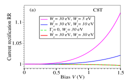
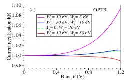
Having said this in general, let us focus on two benchmark junctions fabricated with octanethiol (C8T) and 1, 1’, 4’, 1”-terphenyl-4-thiol (OPT3 in ref. 46) molecules. The parameters , , and that make this analysis possible are available or can be estimated thanks to recent extensive investigations on these monothiolates Xie et al. (2019a, b) as well as on their dithiolate (C8DT Xie et al. (2019b) and OPD3 Xie et al. (2015)) counterparts. Data for dithiols () are also needed because, while providing values of the (geometric) average ,Bâldea (2012b) transport data for a given molecular species do not allow the separate determination of the two individual components and for the presently considered monothiols ().
In view of the fact that not only SAMs deposited on gold but also junctions fabricated with those dithiols are characterized by extremely small statistical variations in their transport properties,Xie et al. (2017) it is legitimate to assume ; dithiolate species form stable covalent bonds responsible for chemisorption both at the substrate and at the tip. In addition, one can assume ; both monothiols and dithiols are linked to substrate by thiol groups. Doing so, based on meV Xie et al. (2019b) and meV Xie et al. (2019b) we get meV and meV. Similarly, using meV Xie et al. (2019a) and meV Xie et al. (2019a) we estimate meV and meV.
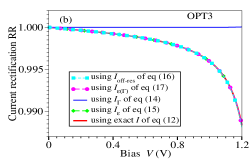
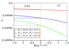
Figures 1 and 2 depict the dependence on bias of the current rectification obtained by using the HOMO offsets derived from recent transport measurements ( eV Xie et al. (2019b) and eV Xie et al. (2019a)) along with the aforementioned values of . As shown by the blue curves of Figures 1b and 2b, the impact of -renormalization brought about by applied bias is completely negligible. The “largest” contribution to rectification comes from the renormalization of the HOMO energy, which is accounted for by Eq. (III) and depicted by the magenta curves. In off-resonant situations and biases of experimental interest this effect is very accurately described by the simpler Eq. (16), which represents the generalization beyond the wide-band approximation of a result (Eq. (4) of ref. 47) deduced earlier in the limit .
To sum up, Figures 1 and 2 clearly reveal that, when fully accounted for, renormalization effects due to MO-couplings to the electrodes of C8T and OPT3 junctions are unable to make RR significantly different from unity and are by no means responsible for the values observed in experiment ( V and V).Xie et al. (2018, 2019a, 2019b) To make this point clearer, in addition to calculations based on parameter values deduced from experimental data (see above), we also performed companion simulations to artificially enhance the impact of the aforementioned renormalization, ruling out that possible parameters’ inaccuracy may vitiate the conclusions presented below. E.g.:
(i) We considered the case of extreme asymmetric couplings to electrodes (). Calculations for this case (green curves in Figures 1a and 2a) yield values of RR that cannot be practically distinguished from unity.
(ii) We performed simulations by using electrode bandwidths substantially smaller than that previously estimated ( eV,Datta et al. (1997); Hall et al. (2000) see above). Letting alone the comparative purpose, the rationale for this choice might be that, unlike practically infinite substrates, more or less sharp tips may have DOS (, cf. eq (6)) different from the value for infinite metal. Notice again that by choosing a smaller -value, renormalization effects are (artificially) overestimated: ’s enter the denominators of relevant formulas, e.g. Eq. (12). Results of these calculations are depicted by the blue and magenta curves in Figures 1a and 2a. The emerging conclusion is the same; although overestimated, this rectification substantially departs from that deduced from experiment and misses any practical relevance.

IV.3 Interrogating Possible Charge Accumulation Effects at Contacts
The exact results reported above in this section have substantiated what the title already stated: the couplings’ asymmetry does not have a quantitatively relevant impact on current rectification. But, after all, this conclusion is based on a highly simplified model. So, one may wonder whether the unequal charge transfer rates may still significantly enhance the completely negligible current asymmetry via physical effects escaping Eq. (1). Being driven by unequal , the effect to be next discussed belongs to this category.
Fabrication of a molecular junction necessarily implies a certain (possibly asymmetric) charge exchange between the embedded molecule and electrodes which cannot be ignored even within a single-electron description Todorov et al. (1993) like that underlying Eq. (1); the level’s energy is renormalized (cf. Eq. (10)) but this is a wispy effect. If significantly dependent on bias polarity, extra electronic charge accumulated at “interfaces” (positions and Eq. (1)) might be relevant in the context of rectification. If this was the case and the MO occupancy significantly changed upon bias polarity reversal, one would have to consider the associated electrostatic interactions (preferably treated within a many-body picture, since this turned out to be feasibleBâldea (2012a)) as a potential source of rectification.
With this in mind, we computed the bias-dependent MO occupancy as well as the occupancies and at the contacts. This is an easy task because, in the absence of electron correlations, the nonequilibrium Keldysh lesser Green’s functions () needed can be straightforwardly expressed in terms of the retarded Green’s functions. Being a rather marginal issue in this paper we skip the technical details; all relevant information can be found in ref. Bâldea, 2016. The results of these calculations using the model parameters deduced in Section IV.2 for C8T are collected in Figure IV.3.
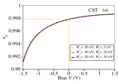

Within the model considered, the differences and visible in Figure IV.3 reflect the combined effect of coupling to electrodes () and applied bias (). The highly localized C8T’s HOMO concentrated in the immediate vicinity of the substrate (e.g, Figure 6 of ref Bâldea, 2015c) makes the impact on “stronger” that that on ; compare Figure IV.3b and Figure IV.3c among themselves. Still, most importantly in the present context, for all biases of experimental relevance, has an altogether negligible impact on all electron occupancies. This rules out any notable contribution to current rectification.
Above, we intentionally restricted ourselves to the case of C8T. The much less spatially asymmetric OPT3’s HOMO delocalized over the entire molecule (e.g., Figure S7 of ref. Xie et al., 2019a) makes the difference in this molecular species even substantially smaller than for C8T.
IV.4 Additional Remarks
We do not want to end this work without commenting on earlier literature attempts to describe the current rectification by postulating a bias-driven energy shift of the single dominant transport channel depending on the coupling to electrodes Cuevas and Scheer (2010); Wang et al. (2011); Briechle et al. (2012); Yuan et al. (2015) as follows
| (18a) | |||
| (18b) |
or equivalently
| (19a) | |||
| (19b) |
Notice that due to the different choice the electric potential origin, and . holds in both cases, implying, e.g., a positive bias on the (ip) for .
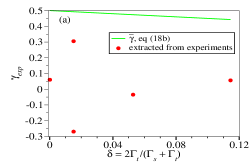
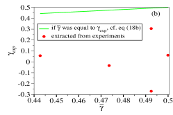
Importantly for checking its validity against experimental data, Eq. (18) predicts that the direction of the MO bias-driven shift (upwards or downwards) is merely dependent on the sign of the couplings’ difference
which translates into a current rectification (RR) direction (i.e., or ) merely dependent on the sign of expressed as follows
and
Although neither deduced theoretically nor validated experimentally, of Eq. (18b) — or the equivalent quantity mentioned above — was utilized in previous publications, e.g., for textbook, illustrative purposes Cuevas and Scheer (2010) or (sometimesWang et al. (2011)) aware of the fact that a asymmetry similar to the asymmetry in the voltage drop is merely an assumption made for the sake of simplicity. The minor difference between Cuevas and Scheer (2010); Wang et al. (2011) and of our Eq. (18b) is due to the different choice the potential origin; the former chose while we used , cf. Eq. (2).
As visible, the never deduced Eq. (18b) has no resemblance with our Eq. (10c), a formula deduced here within a general single level model. Although of little practical importance because we already saw above that the bias-driven MO shift due to and coupling to electrodes expressed by Eq. (10) is altogether negligible, it could still be remarked that even the shift direction of the never-deduced Eq. (18) may be problematic: (cf. Eq. (18b)) as opposed to (cf. Eq. (10c) for ).
By and large, one should conclude that Eq. (18) has no theoretical support. This analytical demonstration adds additional evidence to the fact emphasized earlier that - asymmetry predicted by Eq. (18b) is at odds with various experimental data collected under various platforms; see refs. 57, 23, and citations therein.
Besides the examples presented earlier,Bâldea (2013, 2014) let us demonstrate that the transport data for the presently considered C8T and OPT3 junctions also invalidate Eq. (18). Indeed, inserting the values of and from Section IV.2 into Eq. (18b) we get via for C8T and for OPT3. With of Eq. (18) this translates into for C8T and for OPT3. These values are not only quantitatively but also qualitatively different from the experimental values: Xie et al. (2019b) and .Xie et al. (2019a) For a more complete overview on the unsuitability of Eq. (18), all present and earlier values mentioned above are compiled in Table 1 and depicted graphically in Figure 4.
Put conversely, let us now assume that Eq. (18b) was correct (i.e., ) and applied to the OPT3 junctions considered above. (Remember, this cannot be done for C8T junctions wherein Xie et al. (2019b) would imply and hence, completely unrealistically, a charge transfer rate between the substrate and HOMO located in its close vicinity smaller than the HOMO-tip charge transfer rate across the long alkyl backbone.) With the value extracted from OPT3 --data,Xie et al. (2019a) we get meV. Being substantially smaller than meV (cf. Section IV.2), this value meV is unphysical; located at center of the symmetrical OPD3 molecule, OPD3 HOMO’s center-of-charge is more distant from the substrate than OPT3 HOMO’s center-of-charge displaced from the molecular center towards the thiol end.
| System | |||
|---|---|---|---|
| 0.056 a | 0.115 f | 0.443 g | CP-AFM, OPT3 Xie et al. (2019b) |
| -0.035 b | 0.053 f | 0.474 g | CP-AFM, C8T Xie et al. (2019a) |
| 0.060 c,d | 1.1e-4 c | 0.500 g | EC-STM (variable bias mode), azurin Artés et al. (2012) |
| -0.305 e,d | 0.015 e | 0.492 g | EC-STM (variable bias mode), viologen Pobelov et al. (2008) |
| -0.270 e,d | 0.015 e | 0.492 g | EC-STM (constant bias mode), viologen Pobelov et al. (2008) |
To avoid misunderstandings, one should finally note that in this work emphasis was on the fact that the asymmetric coupling of the dominant level to electrodes () does not give rise to current rectification in most real molecular junctions. This does by no means imply that current rectification cannot be quantitatively described within the single level model. Along with the imbalance between the electrodes’ (electro)chemical potential (Eq. (2)) an applied bias may in general yield a (bias-driven) shift of the energy level
| (20) |
This was quantitatively shown in experimental data analysis,Smith et al. (2018); Xie et al. (2019a, b) with the important observation that the above turned out to be a parameter independent of and which is neither equal to entering Eq. (10c) nor to of Eq. (18b). It is the opposite energy shift direction caused by positive and negative biases that gives rise to rectification, which can be accounted theoretically by means of the single model (cf. Eq. (1))
wherein the -dependence is expressed by Eq. (20). In general, the dependence on of expressed by Eq. (20) results from the interplay between intramolecular Stark effects Xie et al. (2018) and off-center spatial location of MO’s center of charge.Peterson et al. (2001); Zahid et al. (2003); Zhang et al. (2008) The latter (expression of the “lever” Peterson et al. (2001) or “potentiometer” Bâldea (2015c); Xie et al. (2018) rule) results from convoluting the MO’s spatial distribution with the local electric potential whose determination requires to simultaneously (self-consistently) solve the quantum mechanical (Schrödinger) and electrostatic (Poisson) equations. Such microscopic calculations turned out to be successful in quantitatively reproducing RR of OPT3 junctions even subject to a mechanical deformation.Xie et al. (2021) State-of-the-art ab initio calculations Bâldea (2015c); Xie et al. (2018) showed that in alkanethiols the intramolecular Stark effect yields a strictly linear -dependence well beyond the bias range sampled in experiments.Xie et al. (2018, 2019b)
To be on the safe side, we wrote above that cannot yield RR-values significantly different from unity “in most real molecular junctions”. The results deduced in this work showed that this is indeed the case irrespective of whether the charge transport is off-resonant (cf. Eq. (III)) or on-resonant. In situations escaping the model of Eq. (1) — unlikely in real molecules but still possible in artificial nanostructures where electronic properties can be continuously tuned — close to resonance, level’s occupancy may be significantly different from zero and -dependent. Bâldea (2014, 2015a, 2015b, 2015c) If furthermore on-site electron-electron interactions Stafford (1996); Büttiker and Sánchez (2003) or electron-electron interactions at contacts Bâldea (2012a) are strong, may lead to a certain - asymmetry, although spectacular RR-values can hardly be expected on this basis. Problems arise in those cases because, close to resonance, electron couplings both to slow vibrational degrees of freedom (reorganization effects) fast phonons (deserving quantum-mechanical treatment) need be considered.
V Conclusion
It was not our aim here to explain current rectification in real molecular junctions using schematic (tight binding, Hubbard, etc) models extended, e.g., to also include interactions due to charge accumulation at interfaces considered in Section IV.3. Realistic microscopic calculations showed that RR can quantitatively described in real molecular junctions even subject to mechanical stretching Xie et al. (2021) or is situations where, counterintuitively, the dominant MO does not track the substrate in its close proximity but rather the much more distant tip electrode.Bâldea (2015c); Xie et al. (2018)
Rather, in this work, we have presented analytic results deduced theoretically by exactly solving the nonequilibrium problem for a general quantum mechanical Hamiltonian describing the charge transport dominated by a single energy level. Technically speaking, the present study goes beyond the existing approaches to charge transport and related current rectification within a single dominant channel because we worked out the general equation Eq. (11) for the current by employing exact expressions for the embedding self-energies having: (i) nonvanishing real parts (cf. Eq. (8b)) and (ii) imaginary parts that do depend on energy (cf. Eq. (8a)).
The formulas deduced in this way enabled us to obtain numerical estimates based on parameter values both extracted from transport measurements on benchmark junctions or even chosen to simulate rectification enhancement. On this basis, we can definitely rule out that unequal MO couplings to electrodes () make a significant contribution to current rectification in experiments with molecular junctions fabricated so far. This conclusion clearly contradicts some opposite claims in previous literature while confirming other assertions based on intuitive considerations.Datta et al. (1997); Hall et al. (2000)
Hypothetically, could yield (albeit not large but still presumably) observable --asymmetry in case of electrodes possessing extremely narrow conduction bands (low imply large , cf. Eq. (10c)). Artificial nanostructure may be better suited for this purpose because their properties can be tuned easier than those of real molecules. Still, in those cases electron correlations will certainly be very strong and invalidate (Laudauer’s) uncorrelated transport description underlying the vast majority of theoretical studies including the present one.
Acknowledgements
The author gratefully acknowledges financial support from the German Research Foundation (DFG grant BA 1799/3-2) in the initial stage of this work and computational support by the state of Baden-Württemberg through bwHPC and the German Research Foundation through grant no INST 40/575-1 FUGG (JUSTUS 2 cluster).
References
- Aviram and Ratner (1974) A. Aviram and M. A. Ratner, Chem. Phys. Lett. 29, 277 (1974), ISSN 0009-2614, URL http://www.sciencedirect.com/science/article/B6TFN-44W4TKJ-6J/2/b2d82450a0ea71575757c7005f5c95c8.
- Yaliraki and Ratner (1998) S. N. Yaliraki and M. A. Ratner, J. Chem. Phys. 109, 5036 (1998), eprint https://doi.org/10.1063/1.477116, URL https://doi.org/10.1063/1.477116.
- Metzger (1999) R. Metzger, Acc. Chem. Res. 32, 950 (1999), URL https://doi.org/10.1021/ja016696t.
- Nitzan (2001) A. Nitzan, Annu. Rev. Phys. Chem. 52, 681 (2001), eprint http://arjournals.annualreviews.org/doi/pdf/10.1146/annurev.physchem.52.1.681, URL http://arjournals.annualreviews.org/doi/abs/10.1146/annurev.physchem.52.1.681.
- Diez-Peres et al. (2009) I. Diez-Peres, J. Hihath, Y. Lee, L. Yu, L. Adamska, M. A. Kozhushner, I. I. Oleynik, and N. Tao, Nat. Chem. 1, 635 (2009), URL http://dx.doi.org/10.1038/nchem.392.
- Nijhuis et al. (2010) C. A. Nijhuis, W. F. Reus, and G. M. Whitesides, J. Am. Chem. Soc. 132, 18386 (2010), pMID: 21126089, eprint http://dx.doi.org/10.1021/ja108311j, URL http://dx.doi.org/10.1021/ja108311j.
- Parida et al. (2011) P. Parida, S. K. Pati, and A. Painelli, Phys. Rev. B 83, 165404 (2011), URL http://link.aps.org/doi/10.1103/PhysRevB.83.165404.
- Jia and Guo (2013) C. Jia and X. Guo, Chem. Soc. Rev. 42, 5642 (2013), URL http://dx.doi.org/10.1039/C3CS35527F.
- Wickramasinghe et al. (2013) L. D. Wickramasinghe, M. M. Perera, L. Li, G. Mao, Z. Zhou, and C. N. Verani, Angew. Chem. Int. Ed. 52, 13346 (2013), eprint https://onlinelibrary.wiley.com/doi/pdf/10.1002/anie.201306765, URL https://onlinelibrary.wiley.com/doi/abs/10.1002/anie.201306765.
- Yoon et al. (2014) H. J. Yoon, K. C. Liao, M. R. Lockett, S. W. Kwok, M. Baghbanzadeh, and G. M. Whitesides, J. Amer. Chem. Soc. 136, 17155 (2014), 1232.
- Metzger (2015) R. M. Metzger, Chem. Rev. 115, 5056 (2015), pMID: 25950274, eprint http://dx.doi.org/10.1021/cr500459d, URL http://dx.doi.org/10.1021/cr500459d.
- Van Dyck and Ratner (2015) C. Van Dyck and M. A. Ratner, Nano Letters 15, 1577 (2015), pMID: 25706442, eprint http://dx.doi.org/10.1021/nl504091v, URL http://dx.doi.org/10.1021/nl504091v.
- Xiang et al. (2016) D. Xiang, X. Wang, C. Jia, T. Lee, and X. Guo, Chem. Rev. 116, 4318 (2016), pMID: 26979510, eprint http://dx.doi.org/10.1021/acs.chemrev.5b00680, URL http://dx.doi.org/10.1021/acs.chemrev.5b00680.
- Trasobares et al. (2016) J. Trasobares, D. Vuillaume, D. Théron, and N. Clément, Nat. Commun. 7, 12850 (2016), URL https://doi.org/10.1038/ncomms12850.
- Chen et al. (2017) X. Chen, M. Roemer, L. Yuan, W. Du, D. Thompson, E. del Barco, and C. A. Nijhuis, Nat. Nanotechnol. 12, 797 (2017), URL http://dx.doi.org/10.1038/nnano.2017.110.
- Thong et al. (2018) A. Z. Thong, M. S. P. Shaffer, and A. P. Horsfield, Sci. Rep. 8, 9120 (2018), URL https://doi.org/10.1038/s41598-018-27557-0.
- Metzger (2018) R. Metzger, Nanoscale 10, 10316 (2018), URL http://dx.doi.org/10.1039/C8NR01905C.
- Baghbanzadeh et al. (2019) M. Baghbanzadeh, L. Belding, L. Yuan, J. Park, M. H. Al-Sayah, C. M. Bowers, and G. M. Whitesides, J. Am. Chem. Soc. 141, 8969 (2019), pMID: 31072101, eprint https://doi.org/10.1021/jacs.9b02891, URL https://doi.org/10.1021/jacs.9b02891.
- Peterson et al. (2001) I. R. Peterson, D. Vuillaume, and R. M. Metzger, J. Phys. Chem. A 105, 4702 (2001), eprint http://dx.doi.org/10.1021/jp0024571, URL http://dx.doi.org/10.1021/jp0024571.
- Bâldea (2012a) I. Bâldea, Chem. Phys. 400, 65 (2012a), ISSN 0301-0104, URL http://www.sciencedirect.com/science/article/pii/S0301010412000870?v=s5.
- Bâldea (2015a) I. Bâldea, Phys. Chem. Chem. Phys. 17, 15756 (2015a), URL http://dx.doi.org/10.1039/C5CP01805F.
- Bâldea (2015b) I. Bâldea, Phys. Chem. Chem. Phys. 17, 20217 (2015b), URL http://dx.doi.org/10.1039/C5CP02595H.
- Bâldea (2015c) I. Bâldea, Phys. Chem. Chem. Phys. 17, 31260 (2015c), URL http://dx.doi.org/10.1039/C5CP05476A.
- Zhang et al. (2015) G. Zhang, M. A. Ratner, and M. G. Reuter, J. Phys. Chem. C 119, 6254 (2015), eprint http://dx.doi.org/10.1021/jp5093515, URL http://dx.doi.org/10.1021/jp5093515.
- Stafford (1996) C. A. Stafford, Phys. Rev. Lett. 77, 2770 (1996), URL https://link.aps.org/doi/10.1103/PhysRevLett.77.2770.
- Bâldea and Köppel (2010) I. Bâldea and H. Köppel, Phys. Rev. B 81, 193401 (2010), selected for the May 17, 2010 issue of Virtual Journal of Nanoscale Science & Technology, http://www.vjnano.org, URL http://link.aps.org/doi/10.1103/PhysRevB.81.193401.
- Büttiker and Sánchez (2003) M. Büttiker and D. Sánchez, Phys. Rev. Lett. 90, 119701 (2003), URL https://link.aps.org/doi/10.1103/PhysRevLett.90.119701.
- Xie et al. (2018) Z. Xie, I. Bâldea, and C. D. Frisbie, Chem. Sci. 9, 4456 (2018), URL http://dx.doi.org/10.1039/C8SC00938D.
- Todorov et al. (1993) T. N. Todorov, G. A. D. Briggs, and A. P. Sutton, J. Phys.: Condens. Matter 5, 2389 (1993), URL https://iopscience.iop.org/article/10.1088/0953-8984/5/15/010/pdf.
- Todorov (2002) T. N. Todorov, Journal of Physics: Condensed Matter 14, 3049 (2002), URL https://doi.org/10.1088/0953-8984/14/11/314.
- Mahan (1990) G. D. Mahan, Many-Particle Physics (Plenum Press, New York and London, 1990), 2nd ed.
- Caroli et al. (1971) C. Caroli, R. Combescot, P. Nozieres, and D. Saint-James, J. Phys. C: Solid State Phys. 4, 916 (1971), URL http://stacks.iop.org/0022-3719/4/i=8/a=018.
- Jauho et al. (1994) A.-P. Jauho, N. S. Wingreen, and Y. Meir, Phys. Rev. B 50, 5528 (1994).
- Haug and Jauho (2008) H. J. W. Haug and A.-P. Jauho, Quantum Kinetics in Transport and Optics of Semiconductors, vol. 123 (Springer Series in Solid-State Sciences, Berlin, Heidelberg, New York, 2008), second, substantially revised ed., ISBN 978-3.540-73561-2.
- Xue et al. (2001) Y. Xue, S. Datta, and M. A. Ratner, J. Chem. Phys. 115, 4292 (2001), URL http://link.aip.org/link/?JCP/115/4292/1.
- Meir and Wingreen (1992) Y. Meir and N. S. Wingreen, Phys. Rev. Lett. 68, 2512 (1992), URL http://link.aps.org/doi/10.1103/PhysRevLett.68.2512.
- Datta (2005) S. Datta, Quantum Transport: Atom to Transistor (Cambridge Univ. Press, Cambridge, 2005), ISBN ISBN-13: 9780521631457 — ISBN-10: 0521631459.
- Newns (1969) D. M. Newns, Phys. Rev. 178, 1123 (1969).
- Desjonqueres and Spanjaard (1996) M.-C. Desjonqueres and D. Spanjaard, Concepts in Surface Physics (Springer Verlag, Berlin, Heidelberg, New York, 1996), ISBN 3540586229, second edition.
- Peskin (2010) U. Peskin, J. Phys. B: Atom. Molec. Opt. Phys. 43, 153001 (2010), URL http://stacks.iop.org/0953-4075/43/i=15/a=153001.
- Schmickler (1986) W. Schmickler, J. Electroanal. Chem. 204, 31 (1986), ISSN 0022-0728, URL http://www.sciencedirect.com/science/article/pii/0022072886805058.
- Schmickler (2003) W. Schmickler, Chem. Phys. 289, 349 (2003), ISSN 0301-0104, URL http://www.sciencedirect.com/science/article/pii/S0301010403000636.
- Reuter (2010) M. G. Reuter, J. Chem. Phys. 133, 034703 (2010), eprint https://doi.org/10.1063/1.3447960, URL https://doi.org/10.1063/1.3447960.
- Hall et al. (2000) L. E. Hall, J. R. Reimers, N. S. Hush, and K. Silverbrook, J. Chem. Phys. 112, 1510 (2000), URL http://scitation.aip.org/content/aip/journal/jcp/112/3/10.1063/1.480696.
- Xie et al. (2019a) Z. Xie, I. Bâldea, and C. D. Frisbie, J. Am. Chem. Soc. 141, 3670 (2019a), eprint https://doi.org/10.1021/jacs.8b13370, URL https://doi.org/10.1021/jacs.8b13370.
- Xie et al. (2019b) Z. Xie, I. Bâldea, and C. D. Frisbie, J. Am. Chem. Soc. 141, 18182 (2019b), pMID: 31617711, eprint https://doi.org/10.1021/jacs.9b08905, URL https://doi.org/10.1021/jacs.9b08905.
- Bâldea (2012b) I. Bâldea, Phys. Rev. B 85, 035442 (2012b), URL http://link.aps.org/doi/10.1103/PhysRevB.85.035442.
- Datta et al. (1997) S. Datta, W. Tian, S. Hong, R. Reifenberger, J. I. Henderson, and C. P. Kubiak, Phys. Rev. Lett. 79, 2530 (1997), URL http://link.aps.org/doi/10.1103/PhysRevLett.79.2530.
- Xie et al. (2015) Z. Xie, I. Bâldea, C. Smith, Y. Wu, and C. D. Frisbie, ACS Nano 9, 8022 (2015), pMID: 26190402, eprint http://dx.doi.org/10.1021/acsnano.5b01629, URL http://dx.doi.org/10.1021/acsnano.5b01629.
- Nguyen et al. (0) Q. V. Nguyen, Z. Xie, and C. D. Frisbie, J. Phys. Chem. C 0, null (0), eprint https://doi.org/10.1021/acs.jpcc.0c11514, URL https://doi.org/10.1021/acs.jpcc.0c11514.
- Xie et al. (2017) Z. Xie, I. Bâldea, A. T. Demissie, C. E. Smith, Y. Wu, G. Haugstad, and C. D. Frisbie, J. Am. Chem. Soc. 139, 5696 (2017), pMID: 28394596, eprint http://dx.doi.org/10.1021/jacs.7b01918, URL http://dx.doi.org/10.1021/jacs.7b01918.
- Bâldea (2016) I. Bâldea, Beilstein J. Nanotechnol. 7, 418 (2016), ISSN 190-4286, URL http://www.beilstein-journals.org/bjnano/single/articleFullText.htm?publicId=2190-4286-7-37.
- Cuevas and Scheer (2010) J. C. Cuevas and E. Scheer, Molecular Electronics: An Introduction to Theory and Experiment (World Scientific Publishers, 2010).
- Wang et al. (2011) G. Wang, Y. Kim, S.-I. Na, Y. H. Kahng, J. Ku, S. Park, Y. H. Jang, D.-Y. Kim, and T. Lee, J. Phys. Chem. C 115, 17979 (2011), eprint http://pubs.acs.org/doi/pdf/10.1021/jp204340w, URL http://pubs.acs.org/doi/abs/10.1021/jp204340w.
- Briechle et al. (2012) B. M. Briechle, Y. Kim, P. Ehrenreich, A. Erbe, D. Sysoiev, T. Huhn, U. Groth, and E. Scheer, Beilstein J. Nanotechnol. 3, 798 (2012), ISSN 2190-4286.
- Yuan et al. (2015) L. Yuan, N. Nerngchamnong, L. Cao, H. Hamoudi, E. del Barco, M. Roemer, R. K. Sriramula, D. Thompson, and C. A. Nijhuis, Nat Commun 6, 6324 (2015), URL http://dx.doi.org/10.1038/ncomms7324.
- Bâldea (2014) I. Bâldea, Phys. Chem. Chem. Phys. 16, 25942 (2014), URL http://dx.doi.org/10.1039/C4CP04316B.
- Bâldea (2013) I. Bâldea, J. Phys. Chem. C 117, 25798 (2013), eprint http://pubs.acs.org/doi/pdf/10.1021/jp408873c, URL http://pubs.acs.org/doi/abs/10.1021/jp408873c.
- Artés et al. (2012) J. M. Artés, M. López-Martínez, A. Giraudet, I. Díez-Pérez, F. Sanz, and P. Gorostiza, J. Am. Chem. Soc. 134, 20218 (2012), eprint http://pubs.acs.org/doi/pdf/10.1021/ja3080242, URL http://pubs.acs.org/doi/abs/10.1021/ja3080242.
- Pobelov et al. (2008) I. V. Pobelov, Z. Li, and T. Wandlowski, J. Am. Chem. Soc. 130, 16045 (2008), URL http://dx.doi.org/10.1021/ja8054194.
- Smith et al. (2018) C. E. Smith, Z. Xie, I. Bâldea, and C. D. Frisbie, Nanoscale 10, 964 (2018), URL http://dx.doi.org/10.1039/C7NR06461F.
- Zahid et al. (2003) F. Zahid, M. Paulsson, and S. Datta, in Advanced Semiconductors and Organic Nano-Techniques, edited by H. Morkoç (Academic Press, 2003), vol. 3, chap. Electrical Conduction through Molecules, ISBN 0-12-507060-8.
- Zhang et al. (2008) J. Zhang, A. M. Kuznetsov, I. G. Medvedev, Q. Chi, T. Albrecht, P. S. Jensen, and J. Ulstrup, Chem. Rev. 108, 2737 (2008), pMID: 18620372, eprint http://pubs.acs.org/doi/pdf/10.1021/cr068073%2B, URL http://pubs.acs.org/doi/abs/10.1021/cr068073%2B.
- Xie et al. (2021) Z. Xie, I. Bâldea, Q. Nguyen, and C. D. Frisbie, Quantitative Analysis of Weak Current Rectification in Molecular Junctions Subject to Mechanical Deformation Reveals Two Different Mechanisms for Oligophenylene Thiols versus Alkane Thiols (preprint) (2021.