Electrical tuning of tin-vacancy centers in diamond
Abstract
Group-IV color centers in diamond have attracted significant attention as solid-state spin qubits because of their excellent optical and spin properties. Among these color centers, the tin-vacancy (SnV) center is of particular interest because its large ground-state splitting enables long spin coherence times at temperatures above 1 K. However, color centers typically suffer from inhomogeneous broadening, which can be exacerbated by nanofabrication-induced strain, hindering the implementation of quantum nodes emitting indistinguishable photons. Although strain and Raman tuning have been investigated as promising techniques to overcome the spectral mismatch between distinct group-IV color centers, other approaches need to be explored to find methods that can offer more localized control without sacrificing emission intensity. Here, we study electrical tuning of SnV centers in diamond via the direct-current Stark effect. We demonstrate a tuning range beyond 1.7 GHz. We observe both quadratic and linear dependence on the applied electric field. We also confirm that the tuning effect we observe is a result of the applied electric field and is distinct from thermal tuning due to Joule heating. Stark tuning is a promising avenue toward overcoming detunings between emitters and enabling the realization of multiple identical quantum nodes.
I Introduction
Group-IV color centers in diamond have emerged as promising candidates for the implementation of quantum networks Kimble (2008); Wehner et al. (2018) because they retain their optical coherence when integrated with nanophotonic devices Sipahigil et al. (2016); Rugar et al. (2020a); Evans et al. (2016); Wan et al. (2020). These color centers are inversion-symmetric and thus exhibit a vanishingly small permanent electric dipole moment, which mitigates the influence of electric field fluctuations and results in a high frequency stability of their optical transitions Thiering and Gali (2018). Most notably, the negatively charged silicon-vacancy (SiV) center in diamond has been used to implement several quantum information processing applications Evans et al. (2018); Nguyen et al. (2019); Bhaskar et al. (2020). However, the relatively small ground-state splitting (GSS) of SiV centers restricts the long spin coherence of this emitter to millikelvin temperatures. On the other hand, the negatively charged tin-vacancy (SnV) center comprises a heavier group-IV element in a split-vacancy configuration Wahl et al. (2020); Rugar et al. (2019, 2020b); Iwasaki et al. (2017); Görlitz et al. (2020); Rugar et al. (2021). The comparatively large GSS of SnV centers facilitates long spin coherence times at liquid helium temperatures (1 K) because of the reduced phonon-induced decoherence Trusheim et al. (2020).
Quantum networks require multiple identical quantum nodes that emit indistinguishable photons. A significant challenge for solid-state quantum emitters is that each individual emitter experiences a slightly different strain environment, leading to an inhomogeneous distribution of their optical transition frequencies. Because of the aforementioned inversion symmetry, the spread of optical transition frequencies of group-IV color centers can be very narrow in a low-strain environment Rogers et al. (2014); Sipahigil et al. (2014). Nevertheless, in diamond nanostructures, fabrication-induced strain produces a slightly larger inhomogeneous broadening (< 15 GHz) Evans et al. (2016). Therefore, to achieve indistinguishable emission from distinct color centers, precise tuning of optical transition frequencies is essential. Raman Sipahigil et al. (2016); Sun et al. (2018) and magnetic field Evans et al. (2018) tuning have been employed to control the emitter frequency over ranges comparable to this spread. Those techniques, however, either strongly reduce the photon detection rate or cannot be applied locally on several emitters on the same chip to compensate their frequency detuning. Electromechanical tuning offers a potential solution and has enabled the tuning of the transition frequency of waveguide-coupled SiV centers by tens of GHz Machielse et al. (2019); Wan et al. (2020). This technique, however, is limited to freestanding waveguide structures. Applying an electric field could potentially offer an alternative tuning mechanism through the Stark effect. However, because of the predicted first order insensitivity of transitions to electric fields, this approach has not been realized.
In this Letter, we investigate the electric field susceptibility of SnV centers in diamond. We demonstrate reversible tuning of the transition wavelength by more than 1.7 GHz, which is 57 times the natural linewidth of 30 MHz Trusheim et al. (2020). We measure linear and quadratic Stark effect coefficients for SnV centers to be several orders of magnitude smaller than those of non-inversion-symmetric color centers. The remaining linear shift in some emitters may originate from the relatively high strain in our diamond sample, which we infer from the large distribution of transition frequencies ( 270 GHz) of SnV centers in this sample, as previously characterized in Ref. Rugar et al., 2019. Furthermore, we perform careful control experiments to distinguish the tuning achieved through the Stark effect from that resulting from parasitic heating of the diamond sample. Our results, when combined with an initial pre-selection of emitters for nearby transition frequencies, could enable the realization of multi-emitter quantum information processing applications using diamond color centers.
II Fabrication and characterization
We begin our fabrication process with an electronic-grade, single-crystal diamond plate from Element Six. The chip is cleaned in a boiling tri-acid (1:1:1 sulfuric/nitric/perchloric acids) solution. We then remove the top 300 nm of diamond with an oxygen (O2) plasma etch. SnV centers are generated via 120Sn+ ion implantation (370 keV, cm-2) followed by vacuum annealing at 800 for 30 minutes and 1100 for 90 minutes. Based on Stopping Range of Ions in Matter (SRIM) simulations Ziegler et al. (2010), we expect the depth of our SnV centers to be nm.
After generating SnV centers in diamond, we fabricate nanopillars and mesas to easily identify single SnV centers and to increase the photon extraction efficiency. We grow 200 nm of silicon nitride (SixNy) via low-pressure chemical vapor deposition. We pattern square arrays of circles (pillars) separated by rectangles (mesas) in hydrogen silsesquioxane FOx-16 via electron-beam (e-beam) lithography. The circles range in diameter from 140 nm to 300 nm. The rectangles are . The pattern is transferred into the SixNy film by a SF6, CH4, and N2 reactive ion etch. Using the SixNy layer as an etch mask, we perform an O2 plasma etch to fabricate 500-nm tall diamond nanopillars and mesas. Finally, the etch mask is removed by soaking the sample in hydrofluoric acid.
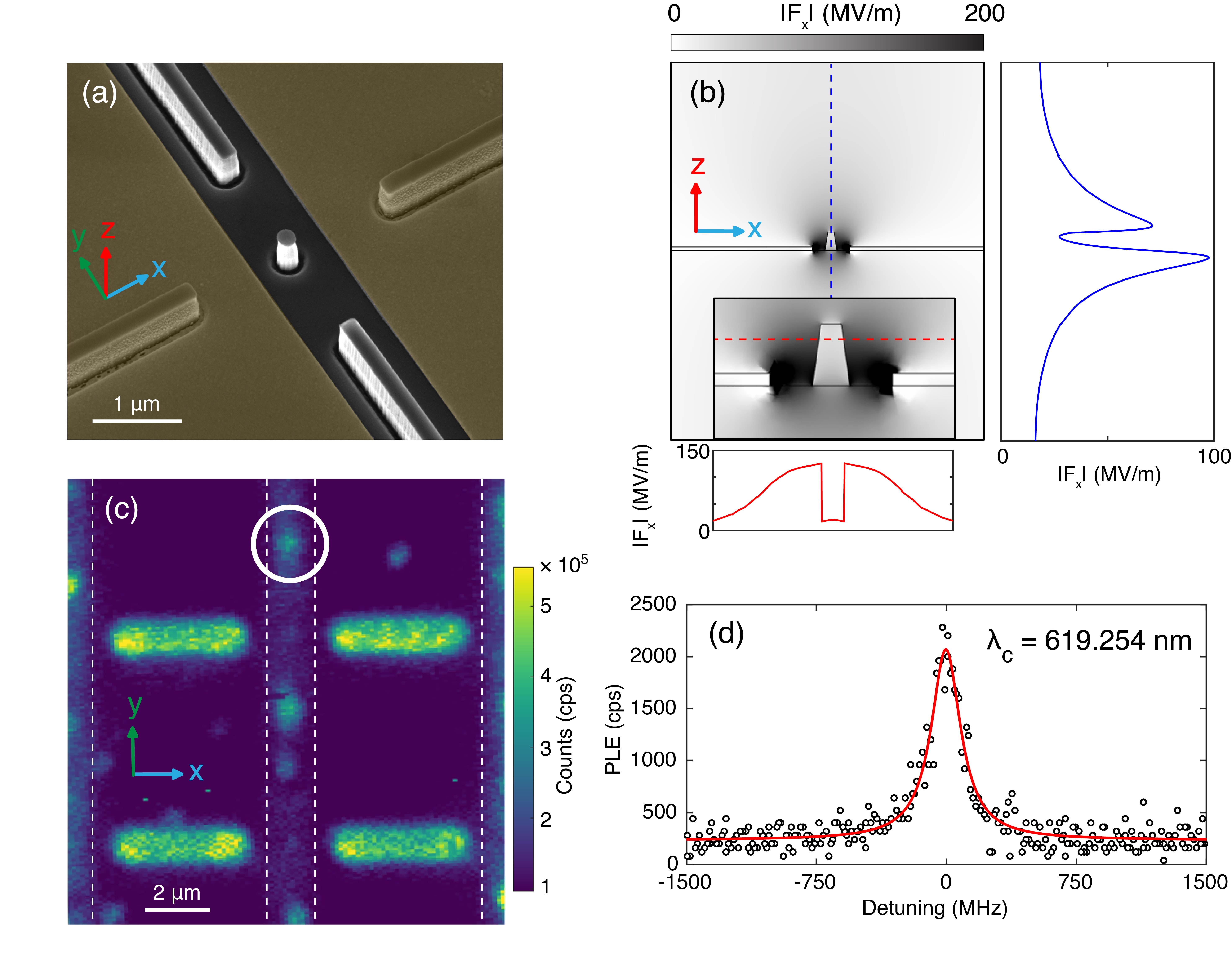
We then fabricate parallel electrodes around a column in an array of nanopillars to produce an electric field along the direction. The 4- wide electrodes are placed 1 apart. The electrodes are created via metal liftoff. Poly(methyl methacrylate) (PMMA) is patterned via e-beam lithography. Then 5 nm of Ti followed by 30 nm of Au are deposited by e-beam evaporation. The remaining PMMA is lifted off in acetone. A scanning electron microscope image of the resulting diamond structures and metal electrodes is shown in Fig. 1(a).
We use the finite element method (COMSOL) to simulate the electric field inside a pillar or a mesa. Fig. 1(b) shows the simulated magnitude of the electric field along the x direction () when 200 V is applied across the electrodes. The inset is a close-up view of the field distribution around the mesa, indicating a lower magnitude in the mesa compared to the bulk region. The right panel in Fig. 1(c) is a vertical line cut through the center of a diamond mesa, showing as a function of z position, while the bottom panel shows as a function of x at the estimated implantation depth. The electric field magnitude is a factor of three smaller at 90 nm below the top of the mesa, than at the surface of diamond for a bulk region.
We perform the optical characterization of SnV centers in this sample at K in a cryostat (Montana Instruments Cryostation). Using a home-built scanning confocal microscope setup, we scan a 532-nm continuous-wave laser across our sample and collect the emission into the SnV center zero-phonon line with a -nm bandpass filter placed in front of a multi-mode fiber to acquire a photoluminescence (PL) map of the region (Fig. 1(c)).
At 5 K, the SnV center has two dominant zero-phonon line transitions often referred to as the C and D transitions Iwasaki et al. (2017). These transitions are centered around 620 nm, and in unstrained SnV centers the C transition is typically 850 GHz higher in energy than the D transition. We perform a photoluminescence excitation (PLE) measurement on the C transition of the emitter circled in Fig. 1(c), which we will refer to as E1, to characterize its resonant frequency and linewidth. We scan the wavelength of a tunable laser (MSquared SolsTiS and External Mixing Module) around the transition wavelength and collect the emission into the phonon sideband (PSB) with a 638-nm long-pass filter and a 700-nm short-pass filter placed before a multi-mode collection fiber. When the laser passes through resonance with the C transition, a peak in the PSB photon counts occurs. To this peak, shown in Fig. 1(e), we fit a Lorentzian curve to find the center wavelength 619.254 nm and linewidth (19412) MHz.
III Voltage-Dependent Photoluminescence Excitation
To investigate the behavior of the SnV center in the presence of an electric field, we apply a direct-current (DC) voltage to the electrodes using a high-voltage power supply (Stanford Research Systems PS325). Fig. 2 shows consecutive PLE scans of the color center E1 as we vary the applied voltage. We observe a reversible redshift in the resonant frequency of the SnV center for both polarities of the electric field. Repeatable tuning of the emission frequency confirms that there is no damage to the SnV even at extremely high electric fields of 50 MV/m.
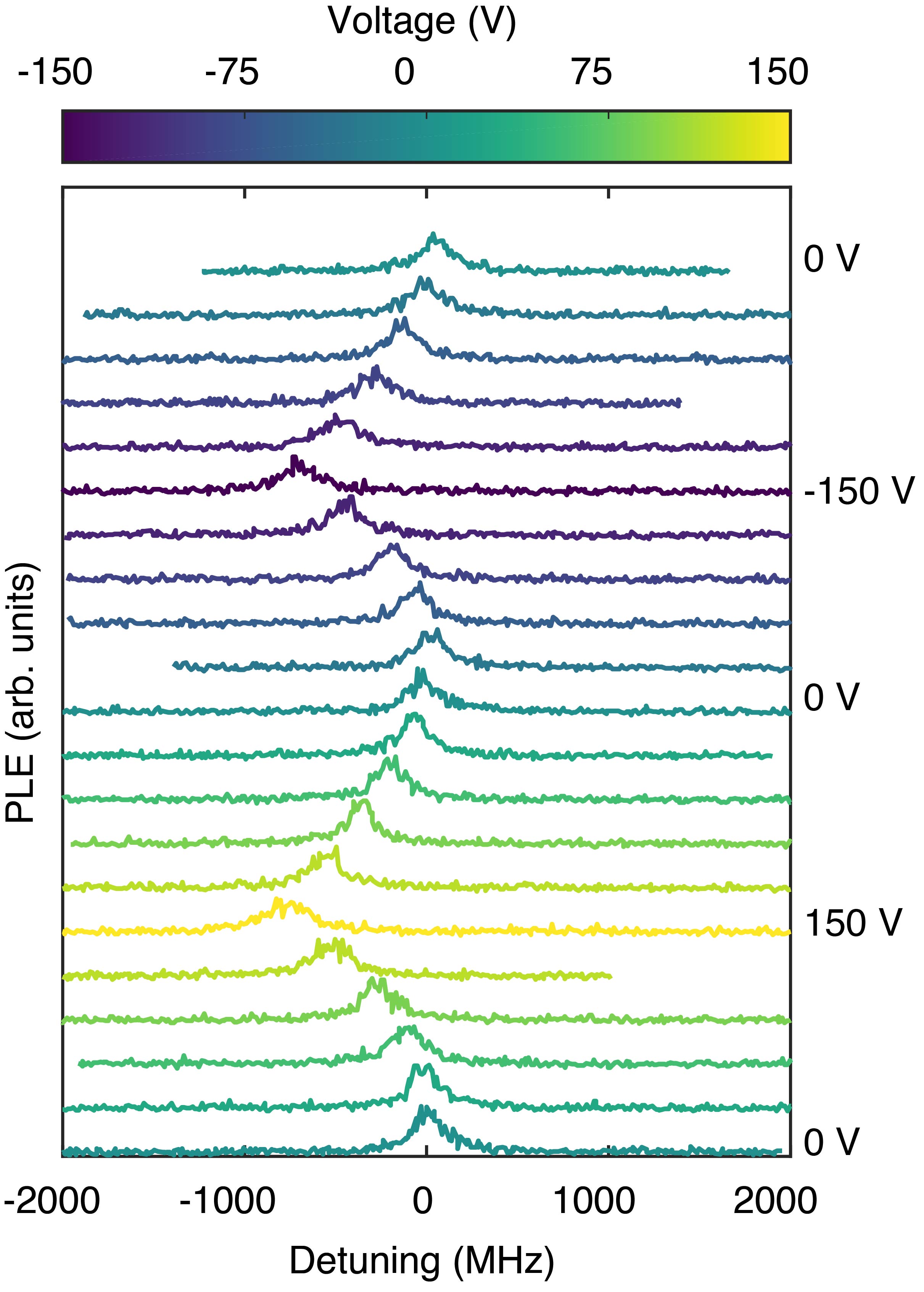
To gain a better understanding of the origin of the shift for single SnV centers, we fit the PLE data in Fig. 2 to a Lorentzian function to extract the shift, linewidth, and the intensity of the signal as we vary the electric field. We approximate the electric field at the location of the emitter using the Lorentz approximation , where is the field extracted from the COMSOL simulations and is the dielectric constant of diamond Tamarat et al. (2006).
III.1 Quadratic shift
Fig. 3(a) shows the extracted shift of the resonance frequency of the SnV center E1 as a function of the applied electric field. We fit the extracted shift () in Fig. 3(a) to a quadratic function of the form where , and are the change in dipole moment and polarizability between the excited and ground states. An inversion-symmetric defect such as the SnV center is expected to have a vanishing , making polarizability the predominant coefficient. From the fit, we extract MHz/(MV/m) which corresponds to D. This value is several orders of magnitude smaller than that of non-inversion-symmetric color centers such as nitrogen-vacancy (NV) centers in diamond Tamarat et al. (2006) and silicon vacancy (V) centers in silicon carbide Lukin et al. (2020). We also obtain MHz/(MV/m)2 which converts to a polarizability volume = 3.28 0.18 . We note that this polarizability volume is four orders of magnitude smaller and has the opposite sign compared to that of NV centers in diamond Tamarat et al. (2006). Most emitters have a positive polarizibility because excited states tend to be more polarizable than ground states Tamarat et al. (2006).
.
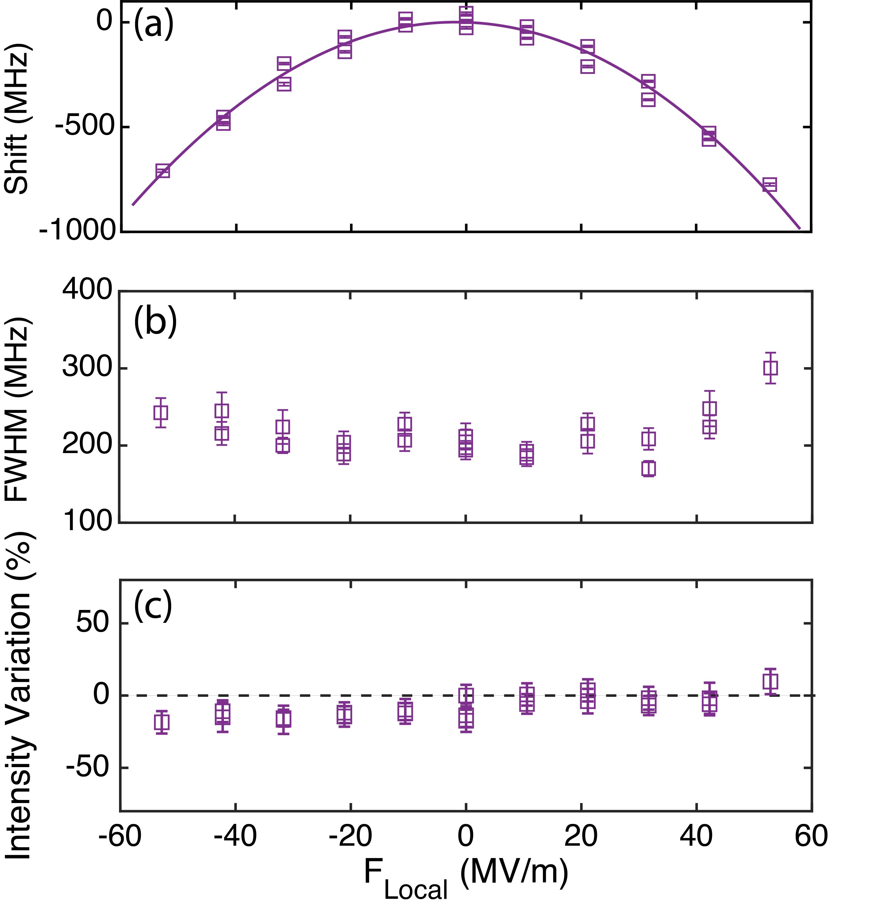
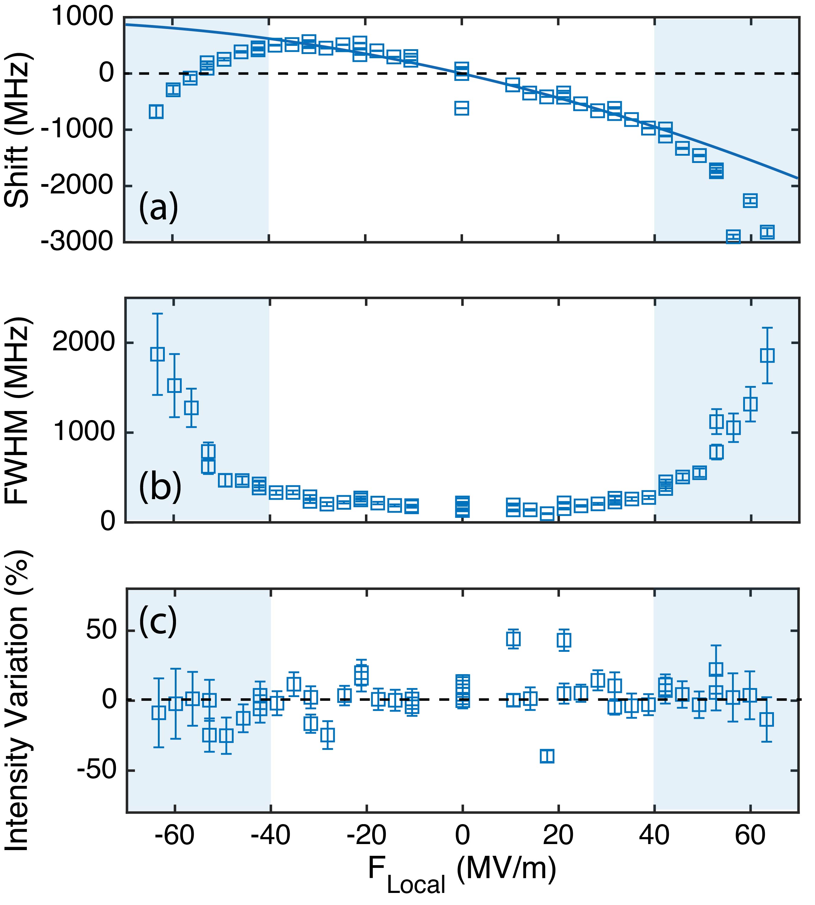
Fig. 3(b) shows the linewidth of the SnV center obtained from the full width at half-maximum (FWHM) of the Lorentzian fits to the PLE data as a function of applied electric field. We observe an increase in the linewidth from the zero-field value of 200 MHz to 300 MHz for the highest electric field. We attribute this increase in linewidth to Joule heating because of the leakage current, as we discuss later. Fig. 3(c) displays the variation in integrated intensity of the PLE signal as a function of the applied electric field. We observe less than 20% variation in the integrated intensity of the signal for a large range of applied electric fields, indicating the potential of this technique as a means to tune SnV centers into resonance with each other.
| No. | (nm) | Linewidth (MHz) | (10-3D) | GSS (GHz) | Shift (GHz) | Type | |
| E1 | 619.254 | 194 12 | 0.19 0.11 | 3.28 0.18 | 819.6 | 0.82 | Quadratic |
| E2 | 619.236 | 132 6 | 3.9 0.4 | 1.19 0.89 | 982.9 | 1.68 | Linear |
| E3 | 619.255 | 126 6 | -0.5 0.5 | 3.8 1.1 | 947.7 | 0.59 | Quadratic |
| E4 | 619.500 | 160 9 | -8.2 1.8 | 5.36 4.05 | 989.4 | 1.73 | Linear |
III.2 Linear shift
We study the electric-field dependence of transition frequency for several other SnV centers. Although a quadratic shift is expected because of the inversion-symmetric structure of this color center, some emitters exhibit a mostly linear shift in transition frequency as a function of applied electric field. Figs. 4(a)-(c) respectively display the extracted shift, linewidth, and intensity variation of PLE spectra for an emitter with mostly linear shift (E2). At local electric field magnitudes greater than 40 MV/m (shaded blue regions), we observe a redshift in the transition frequency and a sharp increase in the SnV linewidth regardless of the field polarity. We attribute this linewidth broadening to Joule heating through leakage current. We observed that the onset voltage for the Joule heating decreased over time, indicating a possible damaged or burned area on the electrodes. In order to extract the Stark parameters without distortions caused by heating, we excluded the data in the shaded region for the fit. The solid blue line in Fig. 4(a) is a fit to the same model as in Fig. 3(a) with extracted parameters D and . This is more than an order of magnitude larger than that of E1 studied in Fig. 3 and could be due to broken inversion symmetry in a strained SnV center. The larger GSS in E2 ( 983 GHz) compared to E1 ( 820 GHz) is another indication of a higher strain environment for E2 Meesala et al. (2018). We repeat this measurement for multiple SnV centers between the electrodes and report the extracted parameters in Table 1.
III.3 Joule heating
To confirm that the observed Stark shift is not related to Joule heating of the color center because of the leakage current, we perform two additional control experiments: we tune a SnV center either (1) by applying a voltage across the electrodes while measuring an emitter outside of the electrode region (E) or (2) by heating the sample and studying E1. We extract the linewidth and resonance frequency of the SnV centers through PLE measurements. In our first control experiment, we study another emitter E that is located outside of the electrode region. Because E is sufficiently far from the electrodes, the DC electric field vanishes and any shift in frequency for this emitter should be due to leakage current, Joule heating, and the high thermal conductivity of diamond. In Figs. 5(a) and (b), we plot the shift and FWHM as functions of the square of the voltage applied across the electrodes (). With Joule heating, the induced temperature change is proportional to the applied voltage squared (), so we use these data to characterize the temperature-dependent behavior of E. We fit a power law model to the data of Figs. 5(a) and (b). From these fits, we find that the thermally induced shift is proportional to and FWHM . This temperature dependence of frequency and FWHM is consistent with previous studies of SiV centers Jahnke et al. (2015). For the second control experiment, we tune the energy of the SnV center studied in Fig. 3 (E1) by heating the cryostat up to 20 K. We plot the detuning and FWHM data of E1 as a function of temperature in Figs. 5(a) and (b). We use the extracted shift of the heated E1 and E to calibrate the proportionality constant between and .
In Fig. 5(c), we plot FWHM as a function of frequency shift for our two control experiments as well as E1 (Fig. 3) and E2 (Fig. 4). We also plot the modeled FWHM against the modeled shift from Figs. 5(a) and (b) as a solid yellow line. The data from the two temperature-tuning control experiments are consistent with each other and exhibit a vastly different behavior from the electrically tuned E1. Furthermore, we can see that at large detunings the slope of the E2 data increases dramatically, approaching the behavior of the thermally tuned emitters. These comparisons prove that while leakage current through electrodes can, in principle, cause Joule heating and broadening of the PLE data, the Stark shifts presented in Figs. 3(a) and 4(a) are not influenced by this effect until very high local fields exceeding 40 MV/m.
IV Conclusions
We have examined the response of the frequency of the C transition of SnV centers in diamond to externally applied electric fields. We can shift the transition frequency by more than 1.7 GHz without introducing a significant broadening of the transition linewidth. We investigate several SnV centers and observe both linear and quadratic dependencies of the shift on the applied electric field. While a quadratic dependence is expected based on the defect’s inversion symmetry, we attribute the linear shift to a small, strain-induced dipole moment. We find changes in dipole moment and polarizability volume between the excited and ground states of up to D and , respectively. Furthermore, we confirm that the observed shift is due to the Stark effect and is distinct from any heating effects by comparing the linewidth versus frequency shift of the emitter when a voltage is applied to that when the stage is heated.
Stark tuning can be used to tune the optical frequency of remote emitters and to control the degree of indistinguishability in two-photon interference experiments of pre-selected emitters Bernien et al. (2012); Sipahigil et al. (2012); Lettow et al. (2010); Patel et al. (2010); Flagg et al. (2010). This technique, which recently enabled the first demonstration of linking three remote NV centers in a quantum network Pompili et al. (2021), may also be applied to group-IV color centers. Group-IV color centers have have very narrow inhomogeneous distribution in bulk Rogers et al. (2014); Sipahigil et al. (2014) and, because of their inversion symmetry, can also have relatively narrow inhomogeneous distributions in nanostructures (< 15 GHz) Evans et al. (2016). Nanophotonic devices hosting two SiV centers with a sub-GHz difference between their transition frequencies have been reported Evans et al. (2018), which is within our Stark tuning range. On this chip, we have also observed sub-GHz frequency detuning between two SnV centers (see Table 1). The 1.7 GHz tuning range that we demonstrate in this Letter is large enough to overcome modest detunings between color centers and enable multi-emitter experiments.
The electric-field dependence of group-IV color centers can be harnessed in other schemes. Modulated electric fields have been proposed as an alternative way to overcome the inhomogeneous broadening of emitters Lukin et al. (2020); Trivedi et al. (2020). This approach would be particularly important for overcoming detunings between closely spaced emitters, for example if the emitters are in the same nanophotonic cavity Lukin et al. (2020); Trivedi et al. (2020). Spectral diffusion presents a challenge when working with group-IV color centers, which require resonant drive for optical spin initialization and control schemes. Feedback-based electric field tuning constitutes a tool for the dynamic stabilization of optical transition frequency of emitters Acosta et al. (2012).
All of these applications of Stark effect-based tuning can be made into more practical options by increasing the achievable Stark tuning range. The Stark tuning range can be further expanded by changing the electrode configuration to increase the field experienced by the emitter. Fabricating electrodes with a narrower gap between them would increase the applied field. Embedding the SnV center below the plane of the electrodes rather than in a nanopillar would increase the field experienced by the emitter a factor of 3. Furthermore, the tuning range can be increased by reducing the voltage-induced heating which allows the application of larger voltages.
In addition to contributing to a deeper understanding of the basic properties of SnV centers, our results pave the way for multi-emitter experiments based on group-IV color centers harnessing Stark shift tuning.
During the preparation of this manuscript, we became aware of a similar, very recent work De Santis et al. (2021).
Acknowledgements.
We are grateful to Daniil Lukin for his experimental assistance to this work. This work is financially supported by Army Research Office (ARO) (award no. W911NF-13-1-0309); National Science Foundation (NSF) RAISE TAQS (award no. 1838976); Air Force Office of Scientific Research (AFOSR) DURIP (award no. FA9550-16-1-0223). S.A. acknowledges support from Bloch postdoctoral fellowship in quantum science and engineering from Stanford Q-FARM. D.R. acknowledges support from the Swiss National Science Foundation (Project P400P2_194424). A.E.R. acknowledges support from the National Defense Science and Engineering Graduate (NDSEG) Fellowship Program, sponsored by the Air Force Research Laboratory (AFRL), the Office of Naval Research (ONR) and the Army Research Office (ARO). C.D. acknowledges support from the Andreas Bechtolsheim Stanford Graduate Fellowship (SGF) and the Microsoft Research PhD Fellowship. Part of this work was performed at the Stanford Nanofabrication Facility (SNF) and the Stanford Nano Shared Facilities (SNSF), supported by the National Science Foundation under award ECCS-2026822.References
- Kimble (2008) H. J. Kimble, Nature 453, 1023 (2008).
- Wehner et al. (2018) S. Wehner, D. Elkouss, and R. Hanson, Science 362, eaam9288 (2018).
- Sipahigil et al. (2016) A. Sipahigil, R. E. Evans, D. D. Sukachev, M. J. Burek, J. Borregaard, M. K. Bhaskar, C. T. Nguyen, J. L. Pacheco, H. A. Atikian, C. Meuwly, R. M. Camacho, F. Jelezko, E. Bielejec, H. Park, M. Lončar, and M. D. Lukin, Science 354, 847 (2016).
- Rugar et al. (2020a) A. E. Rugar, C. Dory, S. Aghaeimeibodi, H. Lu, S. Sun, S. D. Mishra, Z.-X. Shen, N. A. Melosh, and J. Vučković, ACS Photonics 7, 2356 (2020a).
- Evans et al. (2016) R. E. Evans, A. Sipahigil, D. D. Sukachev, A. S. Zibrov, and M. D. Lukin, Physical Review Applied 5, 044010 (2016).
- Wan et al. (2020) N. H. Wan, T.-J. Lu, K. C. Chen, M. P. Walsh, M. E. Trusheim, L. De Santis, E. A. Bersin, I. B. Harris, S. L. Mouradian, I. R. Christen, E. S. Bielejec, and D. Englund, Nature 583, 226 (2020).
- Thiering and Gali (2018) G. Thiering and A. Gali, Physical Review X 8, 021063 (2018).
- Evans et al. (2018) R. E. Evans, M. K. Bhaskar, D. D. Sukachev, C. T. Nguyen, A. Sipahigil, M. J. Burek, B. Machielse, G. H. Zhang, A. S. Zibrov, E. Bielejec, H. Park, M. Lončar, and M. D. Lukin, Science 362, 662 (2018).
- Nguyen et al. (2019) C. T. Nguyen, D. D. Sukachev, M. K. Bhaskar, B. Machielse, D. S. Levonian, E. N. Knall, P. Stroganov, R. Riedinger, H. Park, M. Lončar, and M. D. Lukin, Physical Review Letters 123, 183602 (2019).
- Bhaskar et al. (2020) M. K. Bhaskar, R. Riedinger, B. Machielse, D. S. Levonian, C. T. Nguyen, E. N. Knall, H. Park, D. Englund, M. Lončar, D. D. Sukachev, and M. D. Lukin, Nature 580, 60 (2020).
- Wahl et al. (2020) U. Wahl, J. G. Correia, R. Villarreal, E. Bourgeois, M. Gulka, M. Nesládek, A. Vantomme, and L. M. Pereira, Physical Review Letters 125, 45301 (2020).
- Rugar et al. (2019) A. E. Rugar, C. Dory, S. Sun, and J. Vučković, Physical Review B 99, 205417 (2019).
- Rugar et al. (2020b) A. E. Rugar, H. Lu, C. Dory, S. Sun, P. J. McQuade, Z.-X. Shen, N. A. Melosh, and J. Vučković, Nano Letters 20, 1614 (2020b).
- Iwasaki et al. (2017) T. Iwasaki, Y. Miyamoto, T. Taniguchi, P. Siyushev, M. H. Metsch, F. Jelezko, and M. Hatano, Physical Review Letters 119, 253601 (2017).
- Görlitz et al. (2020) J. Görlitz, D. Herrmann, G. Thiering, P. Fuchs, M. Gandil, T. Iwasaki, T. Taniguchi, M. Kieschnick, J. Meijer, M. Hatano, A. Gali, and C. Becher, New Journal of Physics 22, 013048 (2020).
- Rugar et al. (2021) A. E. Rugar, S. Aghaeimeibodi, D. Riedel, C. Dory, H. Lu, P. J. McQuade, Z.-X. Shen, N. A. Melosh, and J. Vučković, arXiv: 2102.11852 (2021).
- Trusheim et al. (2020) M. E. Trusheim, B. Pingault, N. H. Wan, M. Gündoğan, L. De Santis, R. Debroux, D. Gangloff, C. Purser, K. C. Chen, M. Walsh, J. J. Rose, J. N. Becker, B. Lienhard, E. Bersin, I. Paradeisanos, G. Wang, D. Lyzwa, A. R.-P. Montblanch, G. Malladi, H. Bakhru, A. C. Ferrari, I. A. Walmsley, M. Atatüre, and D. Englund, Physical Review Letters 124, 023602 (2020).
- Rogers et al. (2014) L. Rogers, K. Jahnke, T. Teraji, L. Marseglia, C. Müller, B. Naydenov, H. Schauffert, C. Kranz, J. Isoya, L. McGuinness, and F. Jelezko, Nature Communications 5, 4739 (2014).
- Sipahigil et al. (2014) A. Sipahigil, K. D. Jahnke, L. J. Rogers, T. Teraji, J. Isoya, A. S. Zibrov, F. Jelezko, and M. D. Lukin, Physical Review Letters 113, 113602 (2014).
- Sun et al. (2018) S. Sun, J. L. Zhang, K. A. Fischer, M. J. Burek, C. Dory, K. G. Lagoudakis, Y.-K. Tzeng, M. Radulaski, Y. Kelaita, A. Safavi-Naeini, Z.-X. Shen, N. A. Melosh, S. Chu, M. Lončar, and J. Vučković, Physical Review Letters 121, 083601 (2018).
- Machielse et al. (2019) B. Machielse, S. Bogdanovic, S. Meesala, S. Gauthier, M. J. Burek, G. Joe, M. Chalupnik, Y. I. Sohn, J. Holzgrafe, R. E. Evans, C. Chia, H. Atikian, M. K. Bhaskar, D. D. Sukachev, L. Shao, S. Maity, M. D. Lukin, and M. Lončar, Physical Review X 9, 031022 (2019).
- Ziegler et al. (2010) J. F. Ziegler, M. Ziegler, and J. Biersack, Nuclear Instruments and Methods in Physics Research Section B: Beam Interactions with Materials and Atoms 268, 1818 (2010).
- Tamarat et al. (2006) P. Tamarat, T. Gaebel, J. R. Rabeau, M. Khan, A. D. Greentree, H. Wilson, L. C. L. Hollenberg, S. Prawer, P. Hemmer, F. Jelezko, and J. Wrachtrup, Physical Review Letters 97, 083002 (2006).
- Lukin et al. (2020) D. M. Lukin, A. D. White, R. Trivedi, M. A. Guidry, N. Morioka, C. Babin, Ö. O. Soykal, J. Ul-Hassan, N. T. Son, T. Ohshima, P. K. Vasireddy, M. H. Nasr, S. Sun, J.-P. W. MacLean, C. Dory, E. A. Nanni, J. Wrachtrup, F. Kaiser, and J. Vučković, npj Quantum Information 6, 80 (2020).
- Meesala et al. (2018) S. Meesala, Y.-I. Sohn, B. Pingault, L. Shao, H. A. Atikian, J. Holzgrafe, M. Gündoğan, C. Stavrakas, A. Sipahigil, C. Chia, R. Evans, M. J. Burek, M. Zhang, L. Wu, J. L. Pacheco, J. Abraham, E. Bielejec, M. D. Lukin, M. Atatüre, and M. Lončar, Physical Review B 97, 205444 (2018).
- Jahnke et al. (2015) K. D. Jahnke, A. Sipahigil, J. M. Binder, M. W. Doherty, M. Metsch, L. J. Rogers, N. B. Manson, M. D. Lukin, and F. Jelezko, New Journal of Physics 17, 043011 (2015).
- Bernien et al. (2012) H. Bernien, L. Childress, L. Robledo, M. Markham, D. Twitchen, and R. Hanson, Physical Review Letters 108, 043604 (2012).
- Sipahigil et al. (2012) A. Sipahigil, M. L. Goldman, E. Togan, Y. Chu, M. Markham, D. J. Twitchen, A. S. Zibrov, A. Kubanek, and M. D. Lukin, Physical Review Letters 108, 143601 (2012).
- Lettow et al. (2010) R. Lettow, Y. L. Rezus, A. Renn, G. Zumofen, E. Ikonen, S. Götzinger, and V. Sandoghdar, Physical Review Letters 104, 26 (2010), arXiv:0911.3031 .
- Patel et al. (2010) R. B. Patel, A. J. Bennett, I. Farrer, C. A. Nicoll, D. A. Ritchie, and A. J. Shields, Nature Photonics 4, 632 (2010).
- Flagg et al. (2010) E. Flagg, A. Muller, S. Polyakov, A. Ling, A. Migdall, and G. Solomon, Physical Review Letters 104, 137401 (2010), arXiv:1004.0153 .
- Pompili et al. (2021) M. Pompili, S. L. N. Hermans, S. Baier, H. K. C. Beukers, P. C. Humphreys, R. N. Schouten, R. F. L. Vermeulen, M. J. Tiggelman, L. d. S. Martins, B. Dirkse, S. Wehner, and R. Hanson, arXiv: 2102.04471 (2021).
- Trivedi et al. (2020) R. Trivedi, A. White, S. Fan, and J. Vučković, Physical Review A 102, 033707 (2020).
- Acosta et al. (2012) V. M. Acosta, C. Santori, A. Faraon, Z. Huang, K.-M. C. Fu, A. Stacey, D. A. Simpson, K. Ganesan, S. Tomljenovic-Hanic, A. D. Greentree, S. Prawer, and R. G. Beausoleil, Physical Review Letters 108, 206401 (2012).
- De Santis et al. (2021) L. De Santis, M. Trusheim, K. Chen, and D. Englund, arXiv: 2102.01322 (2021), arXiv:2102.01322 .