Rapid Recombination by Cadmium Vacancies in CdTe
Abstract
CdTe is the largest thin-film photovoltaic technology. Non-radiative electron-hole recombination reduces the solar conversion efficiency from an ideal value of to a current champion performance of . The cadmium vacancy (V) is a prominent acceptor species in p-type CdTe; however, debate continues regarding its structural and electronic behavior. Using ab initio defect techniques, we calculate a negative-U double-acceptor level for V, while reproducing the V-1 hole-polaron, reconciling theoretical predictions with experimental observations. We find the cadmium vacancy facilitates rapid charge-carrier recombination, reducing maximum power-conversion efficiency by over for untreated CdTe — a consequence of tellurium dimerization, metastable structural arrangements, and anharmonic potential energy surfaces for carrier capture.
keywords:
American Chemical Society, LaTeXUCL]Thomas Young Centre and Department of Chemistry, University College London, 20 Gordon Street, London WC1H 0AJ, UK \alsoaffiliation[ICL]Thomas Young Centre and Department of Materials, Imperial College London, Exhibition Road, London SW7 2AZ, UK ICL]Thomas Young Centre and Department of Materials, Imperial College London, Exhibition Road, London SW7 2AZ, UK \alsoaffiliation[Yonsei]Department of Materials Science and Engineering, Yonsei University, Seoul 03722, Republic of Korea UCL]Thomas Young Centre and Department of Chemistry, University College London, 20 Gordon Street, London WC1H 0AJ, UK \alsoaffiliation[Diamond]Diamond Light Source Ltd., Diamond House, Harwell Science and Innovation Campus, Didcot, Oxfordshire OX11 0DE, UK \abbreviationsKeywords?
TOC Graphic
![[Uncaptioned image]](/html/2103.00984/assets/x1.png)
1 Introduction
Cadmium telluride (CdTe) is a well-studied thin-film photovoltaic (PV) absorber, being one of few solar technologies to achieve commercial viability.1 Its ideal electronic band gap and high absorption coefficient have allowed it to reach record light-to-electricity conversion efficiencies of .2, 3, 4 Given that device architectures and large-scale manufacturing procedures have been highly optimized for this technology — a result of several decades of intensive research 5, 2 — further reductions in cost will be heavily-dependent on improvements in photoconversion efficiency.1, 6, 2 Indeed, under the idealized detailed balance model, CdTe has an upper limit of single-junction PV efficiency (based on its electronic bandgap),7 indicating that there is still room for improvement.8, 6, 9, 10, 11
Despite over 70 years of experimental and theoretical research,12, 13, 14, 15, 16, 17, 18, 2, 19 the defect chemistry of CdTe is still not well understood. The unambiguous identification of the atomistic origins of many experimentally-observed spectroscopic signatures remains elusive. Only through clear understanding of defect behavior can strategies be devised to avoid and/or mitigate their deleterious effects on device performance.20, 21, 22, 23
At present, market-leading CdTe solar cells employ a Te-rich p-type CdTe absorber layer, favoring the formation of Cd vacancies. Indeed, undoped CdTe grown from the melt is typically found to exhibit native p-type behavior,14 which has often been attributed to the presence of vacancies in the Cd sub-lattice (and/or Te-on-Cd antisites)18. However, the exact origin of this low intrinsic p-type conductivity is still not well understood, with difficulties in definitive measurements15, 14, 16, 24, and discrepancies between models and observations.2, 25, 26, 27, 28 While there is consensus that the cadmium vacancy (V) is an important acceptor species in CdTe, strong debate has endured regarding its structural and electronic behavior.29, 2, 26, 27, 28, 18, 30, 31, 14, 32
2 Theory
The ability of modern theoretical approaches to accurately describe defect behavior is well-established.20, 33, 34, 35, 33 The use of a sufficiently accurate Hamiltonian is essential for reliable predictions. For CdTe, using a screened hybrid Density Functional Theory (DFT) functional with spin-orbit coupling (HSE+SOC), we find that the room-temperature experimental bandgap of is reproduced at a Hartree-Fock exchange fraction , a value which also reproduces the experimental lattice constant to within (see Supporting Information). For consistency, this model was employed in all structural optimizations and electronic calculations.
3 Results & Discussion
Cadmium Vacancy: Equilibrium Structures. The first step in any theoretical investigation of solid-state defects is the determination of their equilibrium structures. CdTe crystallizes in the zinc-blende structure (space group ), thus exhibiting tetrahedral () symmetry at both the Cd and Te sites. The relaxed geometric configurations upon creation of a cadmium vacancy in the neutral (V0), single-negative (V-1) and double-negative (V-2) charge states are shown in Figure 1. Only the double-negative defect retains the original tetrahedral point-group site symmetry, with a contraction of the neighboring Te atoms from the original bond distance of to from the vacancy center-of-mass.
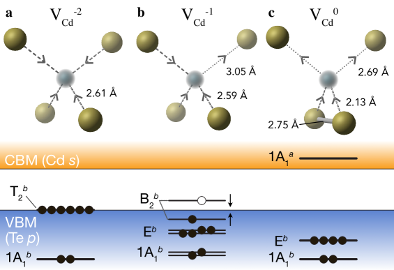
The defect site distortions can be rationalized through consideration of the local bonding behavior in a molecular orbital model.36, 37 Removal of a Cd atom (and its two valence electrons) to create a vacancy results in a fully occupied electron level and a occupied level at the Fermi level, arising from the tetrahedral coordination of Te sp3-hybrid orbitals. In the double-negative case (V-2), the level becomes fully occupied and thus tetrahedral point symmetry is maintained (Figure 1a), with the Te atoms moving closer to the vacancy site to allow for greater hybridization between dangling bonds.
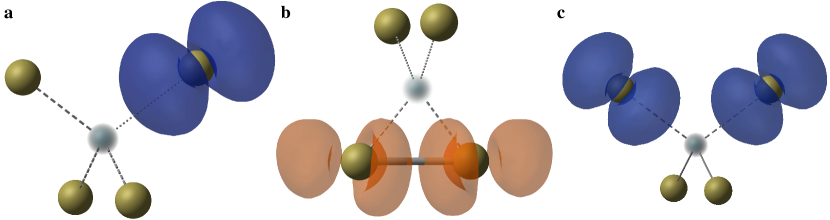
For the singly-charged vacancy, the partial occupancy of the level is unstable, undergoing a trigonal Jahn-Teller distortion that substantially elongates one of the Te neighbor distances (Figure 1b). In this -symmetry vacancy coordination, a positive hole is strongly localized on the Te atom furthest from the vacancy site, as depicted in Figure 2a, resulting in a paramagnetic defect species. This polaronic structure of V-1 was experimentally identified in the 1990s, using electron paramagnetic resonance (EPR),14, 16 but was only reproduced for the first time in a 2015 theoretical study by Shepidchenko et al.38, using the HSE06 functional. The primary reason why previous ab initio works28, 2, 39, 40, 41, 42, 25 have failed to identify this polaronic ground-state structure for V-1 is the spurious electron self-interaction and consequent over-delocalization inherent in standard (semi-)local DFT functionals.43, 44, 20, 45
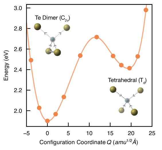
In the neutral case, we find that the Cd vacancy undergoes strong local relaxation to a structural motif, whereby two Te atoms move significantly closer both to the vacancy site and to each other ( separation from an initial )(Figure 1c). This yields a Te dimer arrangement with occupied sp3 -bonding electronic levels deep in the valence band and unoccupied anti-bonding states in the conduction band (Figure 2b). Notably, this Te dimerization resembles that observed at low energy surfaces and grain boundaries in CdTe, and has been suggested as a source of fast recombination at these locations.46, 10, 47 Similar metal-metal dimer reconstructions have been noted for neutral anion vacancies in the II-VI semiconductors ZnSe and ZnS,48 occurring here for the cation vacancy in CdTe due to the metalloid character of the Te anion.
This atomic reconstruction reduces the vacancy formation energy by , relative to the tetrahedral solution that has been widely reported49, 50, 28, 39, 40, 41, 42, 51 — Figures 3 and 4. As with the Jahn-Teller distortion for V-1, this Te dimer equilibrium structure of the neutral vacancy has only recently been identified.18 The tetrahedral and bipolaron (Figure 2c) configurations are in fact local minima on the defect potential energy surface (PES), as shown in Figures 3, 4 and S7.
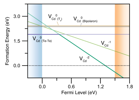
The electronic behavior of the Cd vacancy is dramatically affected by Te dimerisation, as the singly-charged state V-1 is consequently predicted to be thermodynamically unfavorable across all Fermi energies (Figure 4). Accordingly, the vacancy is predicted to act as a so-called negative-U center,52, 53 with a single double-acceptor level at above the valence band maximum (VBM). This is in excellent agreement with experimental reports of a single thermal ionization level in the bandgap at 0.3– above the VBM (Table S1).29, 32, 54, 55, 31, 56, 57, 58 Moreover, negative-U behavior helps to explain apparent discrepancies between experimental reports of Cd vacancy trap levels, as different techniques can measure either the single-charge ( and ) or double-charge transitions ().59 The reasons previous theoretical works have not identified this behavior are twofold; namely, incomplete mapping of the defect potential energy surface (overlooking Te-Te dimerization in V0) and qualitative errors in lower levels of electronic structure theory (destabilizing localized solutions; viz. the V-1 small-polaron) — see Section S6 for further discussion.
3.1 Optical Response
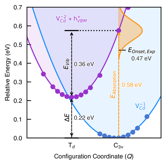
Optical Response. The paramagnetic nature of the single negative charge vacancy V-1 (due to the presence of an odd number of electrons) lends itself to experimental identification through electron spin resonance (ESR/EPR) spectroscopy. In 1993, Emanuelsson et al.14 used photo-ESR to identify the coordination of V-1, with a localized hole on a Te neighbor as predicted here (Figure 2a). After thermal annealing at , they obtained a p-type CdTe film with a carrier concentration p = , in excellent agreement with our predicted maximum hole concentration of p = at this temperature (based on calculated intrinsic defect formation energies). While V-1 is never the lowest energy configuration at equilibrium, we find that Cd vacancies do in fact adopt this charge state under high-temperature p-type growth conditions, as a consequence of energy minimization within the constraint of charge neutrality (to counteract the large hole concentration).
Emanuelsson et al.14 interpreted a decrease in the V-1 ESR intensity upon irradiation with photons of energy as the optical excitation of an electron from the valence band to the () V level, to produce V-2 . Using the defect structures obtained in our investigations, we calculate the peak energy of this transition as , with vibronic coupling estimated to give a Gaussian lineshape with a FWHM of , yielding good agreement with experiment (Figure 5).
3.2 Trap-Mediated Recombination
Trap-Mediated Recombination.
To determine the non-radiative recombination activity, electron and hole capture coefficients were calculated for each charge state of the defect.
This approach, building on the developments of Alkauskas et al.,60 uses the CarrierCapture.jl package61 and full details of the calculation procedure are provided in Section S8.
The PES of the defect is mapped along the structural path (configuration coordinate) between the equilibrium geometries for a given charge transition, from which nuclear wavefunction overlaps can be determined via the 1D Schrödinger equation.62, 60
Electron-phonon coupling is then calculated under static coupling perturbation theory which, in combination with phonon overlaps and scaling factors for charge interaction effects, yields the carrier capture coefficients .
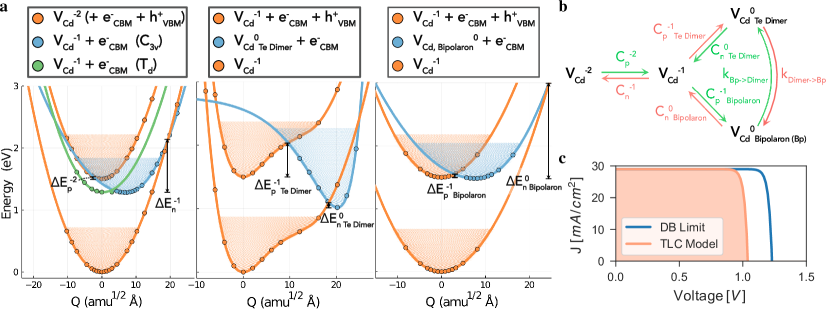
The energy surfaces for all in-gap V carrier traps are shown in Figure 6 and the resulting capture coefficients tabulated in Section S8. As expected for an acceptor defect with a trap level near the VBM (Figure 4), hole capture is fast while electron capture is slow for the (2-/-) transition, with small and large capture barriers, respectively. For the V-1 V0 transitions, however, the behavior is drastically different to that predicted by a simple quantum defect model.63 Firstly, hole capture is more rapid than expected, due to the ability of V-1 to transition to the metastable V0 configuration, before relaxing to the V0 ground-state. Secondly, despite the (-/0) trap level lying over below the CBM (Figure 4), typically implying slow electron capture, we in fact find a giant electron capture coefficient. This unusual behavior is a direct result of the anharmonicity of the PESs at this trap center, accompanied by large electron-phonon coupling, through Te dimer formation. These findings provide additional evidence to support Te dimerization at surfaces and grain boundaries in CdTe as a cause of high recombination velocities at these locations.46, 10, 47 Consequently, the V charge transition is predicted to facilitate rapid electron-hole recombination, proceeding via the {V-1 } {V0 } {V0 } {V-1} cycle shown in Figure 6b. Notably, the large capture coefficients for the rapid (green) processes are comparable to the most deleterious extrinsic defects in silicon64, 65 and the kesterite photovoltaic family.62, 66 This classifies V as a ‘killer center’ 67 and demonstrates the potential impediment of this native defect species to the photovoltaic efficiency of untreated CdTe.
To quantify the effect of this recombination channel on CdTe solar cell performance, we calculate the ‘trap-limited conversion efficiency’ (TLC),66 which incorporates the effects of defect-mediated non-radiative recombination via the Shockley-Read-Hall model.68 This allows us to set an upper limit on the achievable photovoltaic efficiency in the presence of defects. As depicted in the current-voltage curve in Figure 6c, we find that cadmium vacancies can significantly reduce the open-circuit voltage (), minority carrier lifetime () and thus maximum achievable photovoltaic efficiency from the ideal to (for intrinsic p-type CdTe processed under typical anneal temperatures of in a Te-rich atmosphere; see Section S8). Due to the large hole concentrations in the p-type compound, V0 will be the dominant state under steady-state illumination, with electron capture by this defect species representing the rate-limiting step:
Our prediction is a testament to the importance of Cl treatment, strategic impurity doping and Cd-rich growth environments in the fabrication of high efficiency CdTe devices,69, 70, 32, 71, 72, 73, 74, 34, 75, 9, 76, 77, 11, 78, 79 which contribute to the passivation and reduction of cadmium vacancy populations. Notably, the recent achievement of open-circuit voltages surpassing the threshold for CdTe solar cells by Burst et al.11, required a switch to an unorthodox strategy of Cd-rich growth conditions and group V anion doping, reducing the formation of V (and Te).
4 Conclusions
In conclusion, we reconcile several longstanding discrepancies between theoretical predictions and experimental measurements for CdTe, predicting both a single double-acceptor level and the V-1 hole-polaron state for the cadmium vacancy in CdTe. An equilibrium population of cadmium vacancies can facilitate rapid recombination of electrons and holes, reducing the maximum achievable power-conversion efficiency under idealized conditions by over , for untreated CdTe. These recombination kinetics primarily arise from both metastable vacancy structures and the Te dimer configuration of V0 which, in addition to producing negative-U behavior, leads to anharmonic carrier capture PESs. Importantly, these results demonstrate the necessity to include the effects of both metastability and anharmonicity for the accurate calculation of charge-carrier recombination rates in photovoltaic materials.
We thank Dr. Anna Lindström for valuable discussions regarding polaronic structures for cadmium vacancies, and Dr. Sungyhun Kim for assistance with CarrierCapture.jl calculations.
Seán R. Kavanagh acknowledges the EPSRC Centre for Doctoral Training in the Advanced Characterisation of Materials (CDT-ACM)(EP/S023259/1) for funding a PhD studentship.
We acknowledge the use of the UCL Grace High Performance Computing Facility (Grace@UCL), the Imperial College Research Computing Service, and associated support services, in the completion of this work.
Via membership of the UK’s HEC Materials Chemistry Consortium, which is funded by the EPSRC (EP/L000202, EP/R029431, EP/T022213), this work used the ARCHER UK National Supercomputing Service (www.archer.ac.uk) and the UK Materials and Molecular Modelling (MMM) Hub (Thomas — EP/P020194 & Young — EP/T022213).
Computational Methods; Bulk Electronic Structure; Vacancy Bonding, Structural & Electronic Analysis; Discrepancies in Theoretical Studies; Carrier Capture Model, Results & Analysis, Experimental Identification of Tellurium Dimerization; Defect Electronic Densities of States. Data produced during this work is freely available at: \url10.5281/zenodo.4541602.
References
- Zidane et al. 2019 Zidane, T. E. K.; Adzman, M. R. B.; Tajuddin, M. F. N.; Mat Zali, S.; Durusu, A. Optimal Configuration of Photovoltaic Power Plant Using Grey Wolf Optimizer: A Comparative Analysis Considering CdTe and c-Si PV Modules. Solar Energy 2019, 188, 247–257
- Yang et al. 2016 Yang, J.-H.; Yin, W.-J.; Park, J.-S.; Ma, J.; Wei, S.-H. Review on First-Principles Study of Defect Properties of CdTe as a Solar Cell Absorber. Semiconductor Science and Technology 2016, 31, 083002
- 3 Press Release: First Solar Achieves Yet Another Cell Conversion Efficiency World Record (Accessed 11/3/21). investor.firstsolar.com/news/press-release-details/2016/First-Solar-Achieves-Yet-Another-Cell-Conversion-Efficiency-World-Record
- 4 Best Research-Cell Efficiency Chart — Photovoltaic Research — NREL (Accessed 11/3/21). nrel.gov/pv/cell-efficiency.html
- Durose et al. 1999 Durose, K.; Edwards, P. R.; Halliday, D. P. Materials Aspects of CdTe/CdS Solar Cells. Journal of Crystal Growth 1999, 197, 733–742
- Geisthardt et al. 2015 Geisthardt, R. M.; TopiVc, M.; Sites, J. R. Status and Potential of CdTe Solar-Cell Efficiency. IEEE Journal of Photovoltaics 2015, 5, 1217–1221
- Shockley and Queisser 1961 Shockley, W.; Queisser, H. J. Detailed Balance Limit of Efficiency of P-n Junction Solar Cells. Journal of Applied Physics 1961, 32, 510–519
- Pan et al. 2018 Pan, J.; Metzger, W. K.; Lany, S. Spin-Orbit Coupling Effects on Predicting Defect Properties with Hybrid Functionals: A Case Study in CdTe. Physical Review B 2018, 98, 054108
- Ma et al. 2013 Ma, J.; Kuciauskas, D.; Albin, D.; Bhattacharya, R.; Reese, M.; Barnes, T.; Li, J. V.; Gessert, T.; Wei, S.-H. Dependence of the Minority-Carrier Lifetime on the Stoichiometry of CdTe Using Time-Resolved Photoluminescence and First-Principles Calculations. Physical Review Letters 2013, 111, 067402
- Reese et al. 2015 Reese, M. O.; Perkins, C. L.; Burst, J. M.; Farrell, S.; Barnes, T. M.; Johnston, S. W.; Kuciauskas, D.; Gessert, T. A.; Metzger, W. K. Intrinsic Surface Passivation of CdTe. Journal of Applied Physics 2015, 118, 155305
- Burst et al. 2016 Burst, J. M.; Duenow, J. N.; Albin, D. S.; Colegrove, E.; Reese, M. O.; Aguiar, J. A.; Jiang, C.-S.; Patel, M. K.; Al-Jassim, M. M.; Kuciauskas, D.; Swain, S.; Ablekim, T.; Lynn, K. G.; Metzger, W. K. CdTe Solar Cells with Open-Circuit Voltage Breaking the 1 V Barrier. Nature Energy 2016, 1, 1–8
- Castaldini et al. 1998 Castaldini, A.; Cavallini, A.; Fraboni, B.; Fernandez, P.; Piqueras, J. Deep Energy Levels in CdTe and CdZnTe. Journal of Applied Physics 1998, 83, 2121–2126
- Mathew 2003 Mathew, X. Photo-Induced Current Transient Spectroscopic Study of the Traps in CdTe. Solar Energy Materials and Solar Cells 2003, 76, 225–242
- Emanuelsson et al. 1993 Emanuelsson, P.; Omling, P.; Meyer, B. K.; Wienecke, M.; Schenk, M. Identification of the Cadmium Vacancy in CdTe by Electron Paramagnetic Resonance. Physical Review B 1993, 47, 15578–15580
- Kröger 1977 Kröger, F. The Defect Structure of CdTe. Revue de Physique Appliquée 1977, 12, 205–210
- Meyer and Hofmann 1995 Meyer, B. K.; Hofmann, D. M. Anion and Cation Vacancies in CdTe. Applied Physics A: Materials Science & Processing 1995, 61, 213–215
- Meyer et al. 1992 Meyer, B. K.; Omling, P.; Weigel, E.; Müller-Vogt, G. F Center in CdTe. Physical Review B 1992, 46, 15135–15138
- Lindström et al. 2015 Lindström, A.; Mirbt, S.; Sanyal, B.; Klintenberg, M. High Resistivity in Undoped CdTe: Carrier Compensation of Te Antisites and Cd Vacancies. Journal of Physics D: Applied Physics 2015, 49, 035101
- Whelan and Shaw 1968 Whelan, R. C.; Shaw, D. Evidence of a Doubly Ionized Native Donor in CdTe. physica status solidi (b) 1968, 29, 145–152
- Huang et al. 2021 Huang, Y.-T.; Kavanagh, S. R.; Scanlon, D. O.; Walsh, A.; Hoye, R. L. Z. Perovskite-Inspired Materials for Photovoltaics and beyond—from Design to Devices. Nanotechnology 2021, 32, 132004
- Li et al. 2020 Li, Z.; Kavanagh, S. R.; Napari, M.; Palgrave, R. G.; Abdi-Jalebi, M.; Andaji-Garmaroudi, Z.; Davies, D. W.; Laitinen, M.; Julin, J.; Isaacs, M. A.; Friend, R. H.; Scanlon, D. O.; Walsh, A.; Hoye, R. L. Z. Bandgap Lowering in Mixed Alloys of Cs2Ag(SbxBi1-x)Br6 Double Perovskite Thin Films. Journal of Materials Chemistry A 2020, 8, 21780–21788
- Rau et al. 2017 Rau, U.; Blank, B.; Müller, T. C. M.; Kirchartz, T. Efficiency Potential of Photovoltaic Materials and Devices Unveiled by Detailed-Balance Analysis. Physical Review Applied 2017, 7, 044016
- Green 2012 Green, M. A. Radiative Efficiency of State-of-the-Art Photovoltaic Cells. Progress in Photovoltaics: Research and Applications 2012, 20, 472–476
- Meyer and Stadler 1996 Meyer, B. K.; Stadler, W. Native Defect Identification in II–VI Materials. Journal of Crystal Growth 1996, 161, 119–127
- Carvalho et al. 2010 Carvalho, A.; Tagantsev, A. K.; Öberg, S.; Briddon, P. R.; Setter, N. Cation-Site Intrinsic Defects in Zn-Doped CdTe. Physical Review B 2010, 81, 075215
- Menéndez-Proupin et al. 2014 Menéndez-Proupin, E.; Amézaga, A.; Cruz Hernández, N. Electronic Structure of CdTe Using GGA+USIC. Physica B: Condensed Matter 2014, 452, 119–123
- Menéndez-Proupin and Orellana 2016 Menéndez-Proupin, E.; Orellana, W. Theoretical Study of Intrinsic Defects in CdTe. Journal of Physics: Conference Series 2016, 720, 012031
- Wei et al. 2000 Wei, S.-H.; Zhang, S. B.; Zunger, A. First-Principles Calculation of Band Offsets, Optical Bowings, and Defects in CdS, CdSe, CdTe, and Their Alloys. Journal of Applied Physics 2000, 87, 1304–1311
- Takebe et al. 1982 Takebe, T.; Hirata, T.; Saraie, J.; Matsunami, H. DLTS Studies of Deep Levels in Semiconducting N-CdTe Single Crystals. Journal of Physics and Chemistry of Solids 1982, 43, 5–12
- Shepidchenko et al. 2013 Shepidchenko, A.; Mirbt, S.; Sanyal, B.; Håkansson, A.; Klintenberg, M. Tailoring of Defect Levels by Deformations: Te-Antisite in CdTe. Journal of Physics: Condensed Matter 2013, 25, 415801
- Reislöhner et al. 1998 Reislöhner, U.; Grillenberger, J.; Witthuhn, W. Band-Gap Level of the Cadmium Vacancy in CdTe. Journal of Crystal Growth 1998, 184-185, 1160–1164
- Szeles et al. 1997 Szeles, C.; Shan, Y. Y.; Lynn, K. G.; Moodenbaugh, A. R.; Eissler, E. E. Trapping Properties of Cadmium Vacancies in Cd1-xZnxTe. Physical Review B 1997, 55, 6945–6949
- Walsh and Zunger 2017 Walsh, A.; Zunger, A. Instilling Defect Tolerance in New Compounds. Nature Materials 2017, 16, 964–967
- Park et al. 2018 Park, J. S.; Kim, S.; Xie, Z.; Walsh, A. Point Defect Engineering in Thin-Film Solar Cells. Nature Reviews Materials 2018, 3, 194–210
- Scanlon et al. 2009 Scanlon, D. O.; Morgan, B. J.; Watson, G. W.; Walsh, A. Acceptor Levels in P-Type Cu2O: Rationalizing Theory and Experiment. Physical Review Letters 2009, 103, 096405
- Watkins 1976 Watkins, G. Lattice Defects in II-VI Compounds. Radiation Effects in Semiconductors. Dubrovnik, Croatia, 1976; p 95
- Watkins 1996 Watkins, G. Intrinsic Defects in II–VI Semiconductors. Journal of Crystal Growth 1996, 159, 338–344
- Shepidchenko et al. 2015 Shepidchenko, A.; Sanyal, B.; Klintenberg, M.; Mirbt, S. Small Hole Polaron in CdTe: Cd-Vacancy Revisited. Scientific Reports 2015, 5, 1–6
- Du et al. 2008 Du, M.-H.; Takenaka, H.; Singh, D. J. Carrier Compensation in Semi-Insulating CdTe: First-Principles Calculations. Physical Review B 2008, 77, 094122
- Chang et al. 2006 Chang, Y.-C.; James, R. B.; Davenport, J. W. Symmetrized-Basis LASTO Calculations of Defects in CdTe and ZnTe. Physical Review B 2006, 73, 035211
- Lordi 2013 Lordi, V. Point Defects in Cd(Zn)Te and TlBr: Theory. Journal of Crystal Growth 2013, 379, 84–92
- Biswas and Du 2012 Biswas, K.; Du, M.-H. What Causes High Resistivity in CdTe. New Journal of Physics 2012, 14, 063020
- Alberi et al. 2019 Alberi, K. et al. The 2019 Materials by Design Roadmap. Journal of Physics D: Applied Physics 2019, 52
- Butler et al. 2018 Butler, K. T.; Davies, D. W.; Walsh, A. In Computational Materials Discovery; Oganov, A. R., Saleh, G., Kvashnin, A. G., Eds.; Royal Society of Chemistry: Cambridge, 2018; pp 176–197
- Freysoldt et al. 2014 Freysoldt, C.; Grabowski, B.; Hickel, T.; Neugebauer, J.; Kresse, G.; Janotti, A.; Van de Walle, C. G. First-Principles Calculations for Point Defects in Solids. Reviews of Modern Physics 2014, 86, 253–305
- Mönch 2001 Mönch, W. Semiconductor Surfaces and Interfaces, 3rd ed.; Springer Series in Surface Sciences; Springer-Verlag: Berlin Heidelberg, 2001
- Ahr and Biehl 2002 Ahr, M.; Biehl, M. Flat (001) Surfaces of II–VI Semiconductors: A Lattice Gas Model. Surface Science 2002, 505, 124–136
- Lany and Zunger 2004 Lany, S.; Zunger, A. Metal-Dimer Atomic Reconstruction Leading to Deep Donor States of the Anion Vacancy in II-VI and Chalcopyrite Semiconductors. Physical Review Letters 2004, 93, 156404
- Lany et al. 2001 Lany, S.; Ostheimer, V.; Wolf, H.; Wichert, T. Vacancies in CdTe: Experiment and Theory. Physica B: Condensed Matter 2001, 308-310, 958–962
- Chanier et al. 2008 Chanier, T.; Opahle, I.; Sargolzaei, M.; Hayn, R.; Lannoo, M. Magnetic State around Cation Vacancies in II–VI Semiconductors. Physical Review Letters 2008, 100, 026405
- Xu et al. 2014 Xu, R.; Xu, H.-T.; Tang, M.-Y.; Wang, L.-J. Hybrid Density Functional Studies of Cadmium Vacancy in CdTe. Chinese Physics B 2014, 23, 077103
- Watkins 1984 Watkins, G. D. In Advances in Solid State Physics; Grosse, P., Ed.; Springer Berlin Heidelberg: Berlin, Heidelberg, 1984; Vol. 24; pp 163–189
- Coutinho et al. 2020 Coutinho, J.; Markevich, V. P.; Peaker, A. R. Characterisation of Negative- U Defects in Semiconductors. Journal of Physics: Condensed Matter 2020, 32, 323001
- Vul et al. 1973 Vul, B.; Vavilov, V.; Ivanov, V.; Stopachinskii, V.; Chapnin, V. Investigation of Doubly Charged Acceptors in Cadmium Telluride. Soviet Physics Semiconductors - USSR 1973, 6, 1255–1258
- Gippius et al. 1974 Gippius, A. A.; Panossian, J. R.; Chapnin, V. A. Deep-Centre Ionization Energies in CdTe Determined from Electrical and Optical Measurements. Physica Status Solidi (a) 1974, 21, 753–758
- Scholz et al. 1999 Scholz, K.; Stiens, H.; Müller-Vogt, G. Investigations on the Effect of Contacts on P-Type CdTe DLTS-Measurements. Journal of Crystal Growth 1999, 197, 586–592
- Becerril et al. 2001 Becerril, M.; Zelaya-Angel, O.; Vargas-García, J. R.; Ramírez-Bon, R.; González-Hernández, J. Effects of Cd Vacancies on the Electrical Properties of Polycrystalline CdTe Sputtered Films. Journal of Physics and Chemistry of Solids 2001, 62, 1081–1085
- Kremer and Leigh 1988 Kremer, R.; Leigh, W. Deep Levels in CdTe. Journal of Crystal Growth 1988, 86, 490–496
- Wickramaratne et al. 2018 Wickramaratne, D.; Dreyer, C. E.; Monserrat, B.; Shen, J.-X.; Lyons, J. L.; Alkauskas, A.; Van de Walle, C. G. Defect Identification Based on First-Principles Calculations for Deep Level Transient Spectroscopy. Applied Physics Letters 2018, 113, 192106
- Alkauskas et al. 2014 Alkauskas, A.; Yan, Q.; Van de Walle, C. G. First-Principles Theory of Nonradiative Carrier Capture via Multiphonon Emission. Physical Review B 2014, 90, 075202
- Kim et al. 2020 Kim, S.; Hood, S. N.; Puck van Gerwen,; Whalley, L. D.; Walsh, A. CarrierCapture.Jl: Anharmonic Carrier Capture. Zenodo, 2020
- Kim et al. 2019 Kim, S.; Hood, S. N.; Walsh, A. Anharmonic Lattice Relaxation during Nonradiative Carrier Capture. Physical Review B 2019, 100, 041202
- Das et al. 2020 Das, B.; Aguilera, I.; Rau, U.; Kirchartz, T. What Is a Deep Defect? Combining Shockley-Read-Hall Statistics with Multiphonon Recombination Theory. Physical Review Materials 2020, 4, 024602
- Macdonald and Geerligs 2004 Macdonald, D.; Geerligs, L. J. Recombination Activity of Interstitial Iron and Other Transition Metal Point Defects in P- and n-Type Crystalline Silicon. Applied Physics Letters 2004, 85, 4061–4063
- Peaker et al. 2012 Peaker, A. R.; Markevich, V. P.; Hamilton, B.; Parada, G.; Dudas, A.; Pap, A.; Don, E.; Lim, B.; Schmidt, J.; Yu, L.; Yoon, Y.; Rozgonyi, G. Recombination via Point Defects and Their Complexes in Solar Silicon. physica status solidi (a) 2012, 209, 1884–1893
- Kim et al. 2020 Kim, S.; Márquez, J. A.; Unold, T.; Walsh, A. Upper Limit to the Photovoltaic Efficiency of Imperfect Crystals from First Principles. Energy & Environmental Science 2020, 1481–1491
- Stoneham 2001 Stoneham, A. M. Theory of Defects in Solids: Electronic Structure of Defects in Insulators and Semiconductors; Oxford University Press, 2001
- Shockley and Read 1952 Shockley, W.; Read, W. T. Statistics of the Recombinations of Holes and Electrons. Physical Review 1952, 87, 835–842
- Metzger et al. 2019 Metzger, W. K. et al. Exceeding 20% Efficiency with in Situ Group V Doping in Polycrystalline CdTe Solar Cells. Nature Energy 2019, 4, 837–845
- Yang et al. 2015 Yang, J.-H.; Yin, W.-J.; Park, J.-S.; Burst, J.; Metzger, W. K.; Gessert, T.; Barnes, T.; Wei, S.-H. Enhanced P-Type Dopability of P and As in CdTe Using Non-Equilibrium Thermal Processing. Journal of Applied Physics 2015, 118, 025102
- Amarasinghe et al. 2018 Amarasinghe, M.; Colegrove, E.; Moseley, J.; Moutinho, H.; Albin, D.; Duenow, J.; Jensen, S.; Kephart, J.; Sampath, W.; Sivananthan, S.; Al-Jassim, M.; Metzger, W. K. Obtaining Large Columnar CdTe Grains and Long Lifetime on Nanocrystalline CdSe, MgZnO, or CdS Layers. Advanced Energy Materials 2018, 8, 1702666
- Moseley et al. 2018 Moseley, J.; Rale, P.; Collin, S.; Colegrove, E.; Guthrey, H.; Kuciauskas, D.; Moutinho, H.; Al-Jassim, M.; Metzger, W. K. Luminescence Methodology to Determine Grain-Boundary, Grain-Interior, and Surface Recombination in Thin-Film Solar Cells. Journal of Applied Physics 2018, 124, 113104
- Major et al. 2014 Major, J. D.; Treharne, R. E.; Phillips, L. J.; Durose, K. A Low-Cost Non-Toxic Post-Growth Activation Step for CdTe Solar Cells. Nature 2014, 511, 334–337
- Metzger et al. 2003 Metzger, W. K.; Albin, D.; Levi, D.; Sheldon, P.; Li, X.; Keyes, B. M.; Ahrenkiel, R. K. Time-Resolved Photoluminescence Studies of CdTe Solar Cells. Journal of Applied Physics 2003, 94, 3549–3555
- Moutinho et al. 1998 Moutinho, H. R.; Al-Jassim, M. M.; Levi, D. H.; Dippo, P. C.; Kazmerski, L. L. Effects of CdCl2 Treatment on the Recrystallization and Electro-Optical Properties of CdTe Thin Films. Journal of Vacuum Science & Technology A: Vacuum, Surfaces, and Films 1998, 16, 1251–1257
- Kranz et al. 2013 Kranz, L. et al. Doping of Polycrystalline CdTe for High-Efficiency Solar Cells on Flexible Metal Foil. Nature Communications 2013, 4, 2306
- Gessert et al. 2013 Gessert, T. A.; Wei, S. H.; Ma, J.; Albin, D. S.; Dhere, R. G.; Duenow, J. N.; Kuciauskas, D.; Kanevce, A.; Barnes, T. M.; Burst, J. M.; Rance, W. L.; Reese, M. O.; Moutinho, H. R. Research Strategies toward Improving Thin-Film CdTe Photovoltaic Devices beyond 20% Conversion Efficiency. Solar Energy Materials and Solar Cells 2013, 119, 149–155
- Komin et al. 2003 Komin, V.; Tetali, B.; Viswanathan, V.; Yu, S.; Morel, D. L.; Ferekides, C. S. The Effect of the CdCl2 Treatment on CdTe/CdS Thin Film Solar Cells Studied Using Deep Level Transient Spectroscopy. Thin Solid Films 2003, 431-432, 143–147
- Kanevce et al. 2017 Kanevce, A.; Reese, M. O.; Barnes, T. M.; Jensen, S. A.; Metzger, W. K. The Roles of Carrier Concentration and Interface, Bulk, and Grain-Boundary Recombination for 25% Efficient CdTe Solar Cells. Journal of Applied Physics 2017, 121, 214506
See pages - of SI.pdf