Chiral photodetector based on GaAsN
Abstract
The detection of light helicity is key to several research and industrial applications from drugs production to optical communications. However, the direct measurement of the light helicity is inherently impossible with conventional photodetectors based on III-V or IV-VI semiconductors, being naturally non-chiral. The prior polarization analysis of the light by a series of often moving optical elements is necessary before light is sent to the detector. A method is here presented to effectively give to the conventional dilute nitride GaAs-based semiconductor epilayer a chiral photoconductivity in paramagnetic-defect-engineered samples. The detection scheme relies on the giant spin-dependent recombination of conduction electrons and the accompanying spin polarization of the engineered defects to control the conduction band population via the electrons’ spin polarization. As the conduction electron spin polarization is, in turn, intimately linked to the excitation light polarization, the light polarization state can be determined by a simple conductivity measurement. This effectively gives the GaAsN epilayer a chiral photoconductivity capable of discriminating the handedness of an incident excitation light in addition to its intensity. This approach, removing the need of any optical elements in front of a non-chiral detector, could offer easier integration and miniaturisation. This new chiral photodetector could potentially operate in a spectral range from the visible to the infra-red using (In)(Al)GaAsN alloys or ion-implanted nitrogen-free III-V compounds.
I Introduction
In nature, the animal kingdom has developed the ability to detect or reflect circular polarized light (CPL) as an added modality
for enhanced vision, better navigation or “private communications” Rossel1986 ; Cronin2003 ; Tsyr2008 .
The characterization of light polarization states is also essential in a variety of reasearch and industry fields ranging from
pharmaceutics drugs circular dichroism Purdie1996 , polarimetric enhanced vision and imaging Khorasaninejad2006 , spectroscopic material characterization, medical and scientific diagnosis Greenfield2006 ; Sparks7816 and optical
communications Farshchi2011 . The development of a simple, efficient and integrable chiral
photodetector could offer improvements in actual uses but also favour novel device design and applications inspired by natural
vision systems.
The inherent difficulty in discriminating the circular polarization states of light resides in the lack of chirality in
materials commonly employed in optoelectronics. Common (non-chiral) photodetector are thus used in combination with a set of
moving, and often bulky optics such as quarter waveplates and polarizers Berry1977 .
Thus, conventional systems make it a challenge to construct robust, miniature and integrated devices. A direct detection of the
CPL state is a desirable improvement offering advantages in term of robustness and integrability in addition to a simplified
technology. Albeit ultra-compact optical elements for manipulating circularly polarized are actively
investigated Yu2012 ; Gansel2009 , the realization of a simple,
room temperature “single-measurement” circular polarization degree photo-detector remains elusive.
Different approaches have put forward plasmonic or CMOS-like nanostructures meta_1 ; meta_2 ; CMOS or organic chiral
molecules Schulz2019 ; Yang2013 . These devices often suffer from limited acceptance angle and with the use of multiple optical elements
it makes technically challenging to realise miniature and integrated CPL detectors.
Recent measurements on quantum-dots-based hybrid devices have shown a photocurrent helicity asymmetry of 0.4% at
4 K Cadiz2020 , 2% (=4 K) in a similarly designed quantum wells hybrid ferromagnetic/semiconductor structures or again 5.9% in a
Ge-based device (=4 K) Rinaldi2012 . Better results have been reported in chiral plasmonic metamaterials. However, these are absorption devices lacking the direct electrical detection Hovel2008 . Very recently, 2D WTe2 has been used by exploiting the spin photogalvanic effect Ji2020 .
Each of these approaches tackles one or more of the desired characteristics, but suffers some drawbacks such as a narrow spectral range or they do require multiple, complex technological processing steps to be fabricated.
Here we implement the simple solution to this challenge recently proposed in kunold-theory which makes use of a dilute nitride
GaAsN semiconductor epilayer as the spin photoconductive device capable of determining directly, by a voltage or current
measurement, the handedness of an incident light. The device operation relies on the spin dependent recombination of conduction electrons and on the hyperfine interaction (HFI) between bound electrons and nuclei on paramagnetic centers
to provide the device with respectively a sensitivity to the degree of circular polarization and its handedness.
This semiconductor belongs to the family of dilute nitride materials consisting of a GaAs-based semiconductor where a
small percentage of N is introduced to induce the formation of Ga2+ interstitial paramagnetic defects which display both an
exceptionally large spin dependent recombination (SDR) for conduction band electrons and a defect nuclear hyperpolarization
at room temperature sdr1 ; Lombez2005 ; wang_room-temperature_2009 ; Kalevich2012 . A very efficient defect recombination is usually an undesirable feature for optoelectronics devices.
However, as the capture rate is here
dependent on the spin polarization of the conduction band
electrons, it provides a way of controlling the conduction band population and thus the conductivity via the spin polarization.
Key to this device workings is the fact that this spin polarization is likewise transferred not only to the defect-bound
electron but also to the surrounding nuclei via a concomitant action of the hyperfine interaction and dipole-dipole spin
relaxation kunold2020 . This yields a sizeable effective nuclear magnetic field whose
direction is parallel to the conduction electron spin polarization and thus to the photon helicity.
This phenomenon is however equally efficient for spin up or spin down conduction electron polarization allowing only the
determination of a circular polarization degree without its handedness. By exploiting in addition the interplay between
the HFI and a small external magnetic field, the GaAsN epilayer acquires a chiral photoconductivity (PC) capable of discriminating the
handedness of an incident light in addition to a linearly polarized one as demonstrated below.
It is important to note that spin dependent recombination and nuclear polarization can occur on many defects and in various
materials but typically with a weak efficiency or at cryogenic temperatures. In contrast, in GaAsN-based semiconductors they
manifest with macroscopic record-high values at room temperature, paving the way to a practical exploitation of the
phenomenon.
In addition, these paramagnetic defects can be induced to the whole range of GaAs-based alloys from AlGaAsN to
InGaAsN sdr1 , thus allowing a wide range of wavelength operation from the visible to the infra-red spectral region.
Nitrogen-free gallium-ion implanted semiconductor
systems have also been shown to display this giant spin-dependent recombination, allowing dissociating the spin dependent
recombination efficiency and the defect density from the material gap and to offer extended
device configurations and applicabilities Nguyen2013 . Finally, as the the working principle relies on the creation of a spin polarized conduction-band
population, the device’s working range can in principle cover a wide spectrum of excitation wavelength as long as a minimum optical orientation in the conduction band can be achieved.
II Results and Discussion
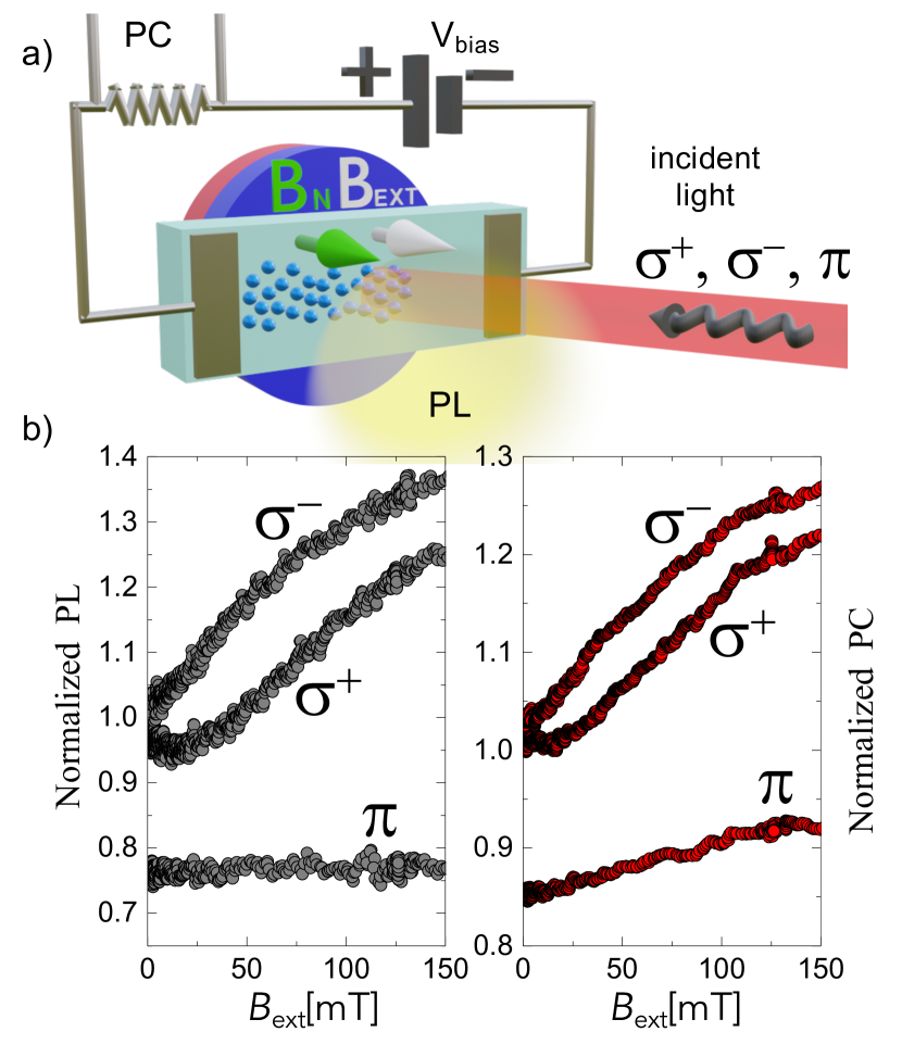
Figure 1b presents the simultaneous measurement of the PL and PC of a GaAsN (2.1% N) sample for different light polarization states as
a function of the applied external magnetic field in Faraday geometry for a 20 mW excitation at 852 nm.
We can see a very similar behaviour for PL and PC as a function of the magnetic field and light polarization,
confirming that the same physical phenomena underpin both measurements.
From these data two features can be noted: (i) The conduction electron population, as revealed by the PL or PC intensities, depends on
the incident light helicity as soon as 0 and for a very small magnetic field strength. This weak field rules out any
macroscopic Zeeman effect on the conduction or defect electron states capable of producing a thermal spin population.
(ii) The asymmetry persists for a large range of magnetic fields (the PL and PC intensities under circular polarization
are expected to eventually become identical for mT kunold-theory ).
These data identify a broad range in external magnetic field where the discrimination of the light polarization can be achieved
and used in a single-reading electrical detection.
The particular dependence of the PL and PC signals as a function of the external magnetic field for different polarization
has been successfully interpreted in the framework of an interplay between the hyperfine interaction (where
is the hyperfine interaction constant)
between the Ga2+ nuclei (spin =3/2) and the bound
electrons (spin =1/2), and the Zeeman interaction induced by the external magnetic field. The hyperfine interaction reduces the SDR efficiency due to the
mixing of the electron’s and nucleus’s spins Ivchenko2015 , but allows for the flow of angular
momentum transfer from the conduction band electron to the defect nucleus in combination with the SDR ibarra-Sierra2017 .
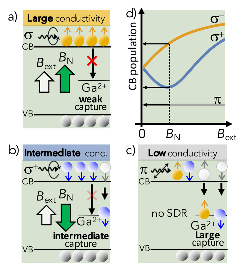
The way this interplay is exploited can be clarified with the help of figure 2 and 3: When the spin of the conduction electrons
shows a preferential orientation (such as under an at least partially circularly polarized light, figure 2a) the defect resident electron
acquires the same spin orientation, through the spin dependent recombination, in a few tens of picoseconds sdr1 .
This spin polarization is likewise transferred to the defect nucleus and neighbouring nuclei through a combination of the
hyperfine interaction and dipole relaxation, yielding an effective nuclear magnetic field . This spin polarization transfer
from the conduction band to the defect electron and nuclear spins has a fundamental role: (i)
by forcing the same spin orientation onto the defect resident electron, it prevents any further conduction electron capture thanks
to the Pauli’s principle. The capture of the conduction electrons is greatly reduced giving the sample a “Large” conduction
population. Without an external magnetic field this happens with the same efficiency for a right or left circular excitation.
Instead, under a linearly-polarized excitation (figure 2c) an equivalent density of spin-up and spin-down conduction population is
photo-generated and no net transfer of spin polarization to the defects can occur.
The conduction capture is no more spin-dependent and the
defect can efficiently capture the conduction electrons leading to a “Low” conduction population.
(ii) Under a weak external magnetic field in Faraday geometry, the PL (or PC) intensity under a circularly polarized light
takes the form of an inverted Lorentzian (figure 2d) ibarra-Sierra2017 displaced from the origin in opposite
direction for a right or left circular incident
polarization due to the presence of the nuclear field which adds up to the external field.
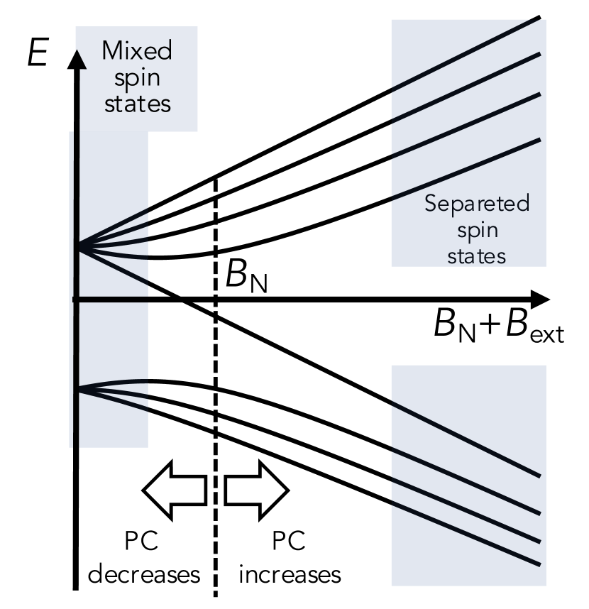
Now the system is effectively chiral: When is parallel or antiparallel to an applied external magnetic field of comparable
strength, the HFI in the defect system is proportionally weakened or strengthened with respect to the electron Zeeman effect
offering a way to proportionally control the SDR efficiency (figure 3). The conduction carrier capture time (figure 2a and b) becomes
dependent on the total magnetic field . As the sign of is directly linked to the
average conduction electrons spin orientation, the sample conductivity becomes now dependent on the average conduction
electrons spin orientation and therefore on the light polarization state incident on the sample.
In more details, the device works on the following principle: A permanent magnet with a field of 30 to 50 mT is placed on the substrate
side of the GaAsN epilayer to have the field parallel (or anti-parallel) to the optical axis of the incident light. The magnetic
field is chosen such that it falls in the optimum region for the discrimination between a circular
right or left incident polarization kunold-theory , which is of the same order of magnitude as .
A constant voltage in the range 0.1 to 4 V is applied to the sample contacts. At this point, the
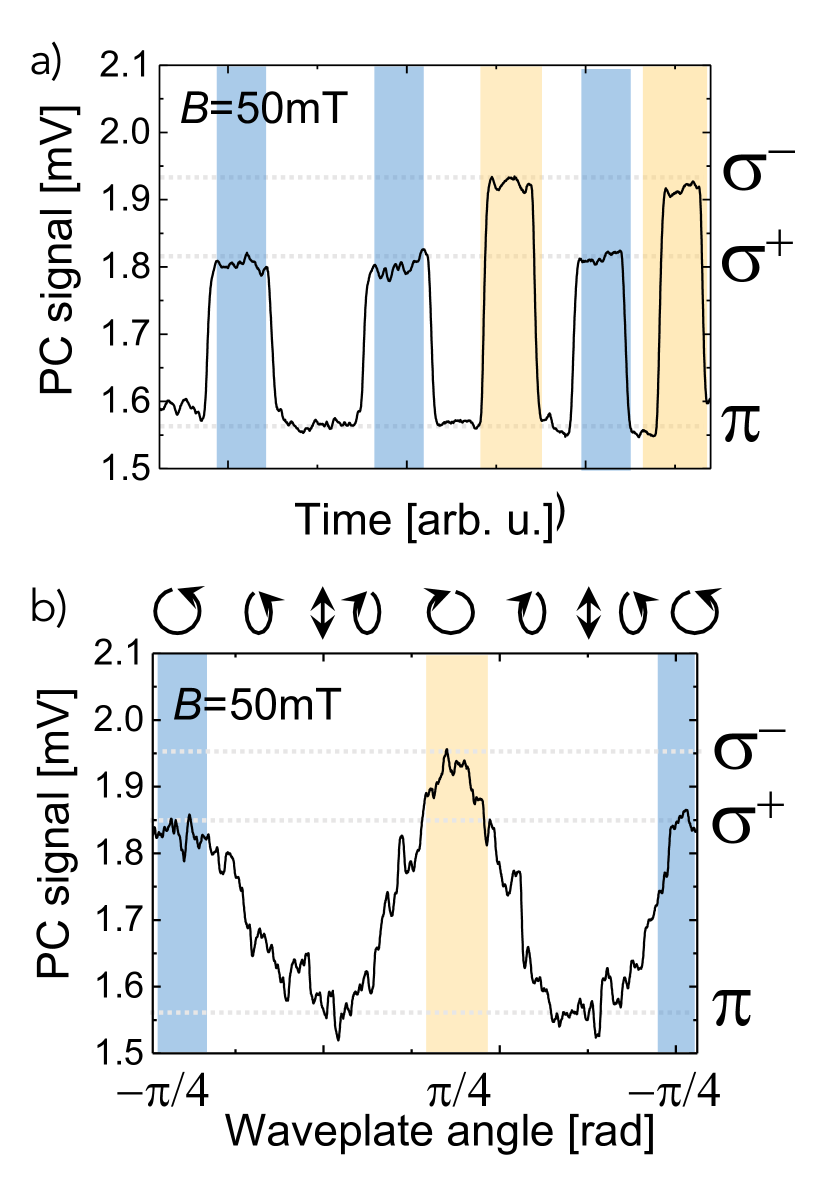
reading of the photoconductivity value reflects the polarization state of the incident light. Figure 4a presents such a
measurement in the case of a 30 mW incident light at 852 nm under the 50 mT magnetic field. We observe a clear difference
between the signal measured for a right, left or linear incident polarization, which allows for the determination of
the light helicity with a simple PC reading. Figure 4b shows how the signal varies when the incident polarization is continuously
modified from right
circular to linear and to left circular by turning the angle of the quarter-wave plate in the incident optical path. This shows in addition that, albeit for a small polarization interval, the device can also determine the
polarization degree of an incident light in a single measurement. Considering that the root mean square error mV as measured from a linear fit of the first plateau signal for a excitation in figure 4a, and the signal difference between a linear and excitation, 0.36 mV, we can estimate a measurement of a circular polarization degree with a precision of about 2% in this proof of concept device.
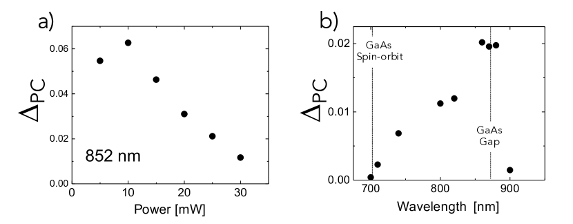
We have characterized the PC contrast ( indicates respectively the PC under a or excitation) as a function of the incident wavelength and power. Figure 5a reports the data obtained as a function of the SDR ratio at =0, SDR, by varying the incident power. The contrast reaches a maximum for a relatively weak powers and then monotonically decreases as the power is increased. This behaviour is well accounted for kunold-theory at low power by the power threshold for the build-up of the nuclear magnetic field. Increasing the excitation power beyond the optimum leads to a decrease of the SDR, leading in return to a decrease of the photocurrent contrast. Figure 5b presents the PC contrast as a function of the excitation wavelength. A constant incident power = 20 mW has been used here for the whole spectral range explored. We can deduce that for this Nitrogen content and for this simple photoconductivity configuration, the device can be used over 100 nm range. The hight wavelength limit (= 870 nm, = 1.424 eV) is due to the change in the absorption coefficient of the device once the excitation energy is smaller than the GaAs gap energy. Exciting with photon energies above the GaAs gap allows instead for a larger absorption of the incoming light as this can occur over the thicker GaAs buffer layer and not only on the thin 100 nm GaAsN one, while preserving a substantial conduction electron spin polarization during the thermalisation and diffusion into the GaAsN layer sipe . No higher excitation wavelength has been tested. However, thanks to the optical selection rules, a PC contrast should in principle be observable for wavelengths up to the GaAsN gap as the conduction spin polarization will increase for excitations closer to the gap, albeit higher powers will be necessary to compensate for the lower absorption in the thin layer. The low wavelength limit (= 704 nm, = 1.76 eV) is instead linked to the onset of the spin-orbit band where no or very weak conduction spin polarization can be achieved. It is important also to consider here that both the absorption coefficient and the photogenerated conduction spin polarization are wavelength dependent. As the SDR depends on the absorbed power and the spin polarization achieved at the bottom of the conduction band, the relation between the PC contrast and wavelength is non-linear.
As suggested in kunold-theory an improved version of the device could be envisaged in the form of either a balanced photodetector composed of two slabs of GaAsN each subject to opposite magnetic fields and . A common voltage source is used to drive in both GaAsN slabs and the measured PCs from the two photodetectors are subtracted. In this configuration, the sign and not the magnitude of the resulting current will reveal the polarization state of the incident light. An alternative solution is also proposed where the differential measurement is obtained in a single GaAsN layer subject to an alternating magnetic field produced by a micro-coil powered by an alternating current (figure 6a). In order to make a proof of concept, we have tested a modified version of the second device design where the single GaAsN is here subject to a constant magnetic field while the incident light has a periodically varying polarization state (figure 6b). The polarization modulation is obtained by rotating a quarter-wave plate at a frequency . In this configuration, the polarization state after the waveplate will periodically change from linear to circular right, linear, circular left and back to linear, twice per rotation. By demodulating the measured photocurrent at a frequency using a lock-in amplifier, the resulting signal is proportional to , i.e. the difference in the photocurrent signal between a circular right and circular left polarized excitation.
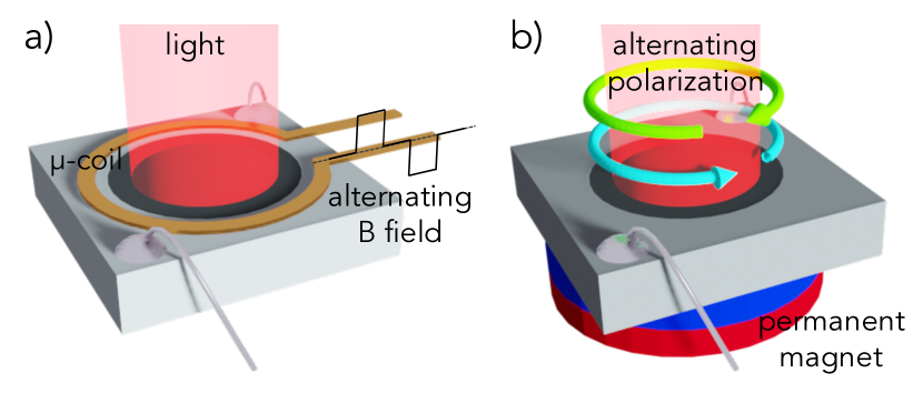
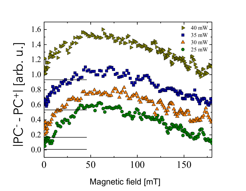
Figure 7 reports the direct measurements of the difference between a circular right and circular left
incident polarization using the set-up presented above, as a function of the excitation power at 852 nm for 25 - 40 mW and
= 21 Hz.
We observed that a sizeable differential signal can be obtained for a large range of external magnetic fields.
In the differential configuration the signal will be different than zero only for circularly polarized light and the limit to the minimum measurable circular polarization degree will be set mainly by the noise equivalent signal of the reading.
This is expected to be greatly improved with a photodiode design instead of a photoconductor one.
A linear or unpolarized light will give instead a zero reading.
III Conclusions
In conclusion, we have shown that leveraging the giant spin dependent recombination and the hyperpolarization of Ga2+ interstitial defect in dilute nitrides epilayers allows for the realization of a chiral III-V dilute nitride semiconductor useable for the direct electrical measurement of the incident light helicity at room temperature. As the working principle relies on the optical orientation of conduction electrons, the working spectral range could be easily extended for wavelengths up to the material band gap and as long a non zero spin polarization of photoexcited electrons can be achieved. This paradigm, enabled by the presence of Ga paramagnetic defects in dilute nitrides, can in principle be extended to the whole family of (In)(Al)GaAsN alloys with gaps ranging from the visible to the infrared. The possibility of producing interstitial defects by implantation in N-free alloys Nguyen2013 could also provide further application possibilities.
IV Methods
The sample studied for the proof of principle demonstration consists of a nm thick
GaAs1-xNx epilayer () grown by molecular beam epitaxy on a (001) semi-insulating GaAs substrate and
capped with nm GaAs. The room temperature gap is at 1080 nm. The excitation light was provided by either a 852 nm laser diode or a continuous wave Ti:Sa laser as the
tunable wavelength source.
The lasers were focused to a 100 m diameter spot (FWHM), in between two Ag electrodes deposited onto the
sample surface about 1 mm apart (figure 1a). The laser light polarization was controlled by a Glan-Taylor polarizer followed by a quarter
wave plate. The laser intensity was modulated by a mechanical chopper at 170 Hz. The sample photoconductivity
(PC) was measured synchronously using a lock-in amplifier from the voltage drop at the terminals of a 1 M load
resistor placed in series with the sample. We have carefully focused the laser in order to avoid any spurious effects related to
the contact illumination. A constant voltage has been applied between the sample electrodes to perform the PC reading.
The photoluminescence (PL) intensity was simultaneously measured with the same lock-in technique by recording its total
intensity, filtered of the laser scattered light and substrate contribution using a series of long-pass optical filters, and integrated by
an InGaAs photodiode. A permanent Neodymium magnet has been used to apply a magnetic field in the Faraday geometry and
the field strength on the sample surface has been varied by changing the magnet’s distance from the sample. All the experiments
were performed at room temperature.
References
- (1) S. Rossel, R. Wehner, Nature 1986, 323 128.
- (2) T. W. Cronin, N. Shashar, R. L. Caldwell, J. Marshall, A. G. Cheroske, T.-H. Chiou, Integrative and Comparative Biology 2003, 43, 4 549.
- (3) T.-H. Chiou, S. Kleinlogel, T. Cronin, R. Caldwell, B. Loeffler, A. Siddiqi, A. Goldizen, J. Marshall, Current Biology 2008, 18 429.
- (4) N. Purdie, J. Am. Chem. Soc. 1996, 118, 50 12871.
- (5) M. Khorasaninejad, W. T. Chen, A. Y. Zhu, J. Oh, R. C. Devlin, D. Rousso, F. Capasso, Nano Letters 2006, 7, 16 4595.
- (6) N. J. Greenfield, Nature Protocols 2006, 1, 6 2876.
- (7) W. B. Sparks, J. Hough, T. A. Germer, F. Chen, S. DasSarma, P. DasSarma, F. T. Robb, N. Manset, L. Kolokolova, N. Reid, F. D. Macchetto, W. Martin, Proceedings of the National Academy of Sciences 2009, 106, 19 7816.
- (8) R. Farshchi, M. Ramsteiner, J. Herfort, A. Tahraoui, H. T. Grahn, Applied Physics Letters 2011, 98, 16 162508.
- (9) H. G. Berry, G. Gabrielse, A. E. Livingston, Appl. Opt. 1977, 16, 12 3200.
- (10) N. Yu, F. Aieta, P. Genevet, M. A. Kats, Z. Gaburro, F. Capasso, Nano Letters 2012, 12 6328.
- (11) J. K. Gansel, M. Thiel, M. S. Rill, M. Decker, K. Bade, V. Saile, G. von Freymann, S. Linden, M. Wegener, Science 2009, 325, 5947 1513.
- (12) W. Li, Z. J. Coppens, L. V. Besteiro, W. Wang, A. O. Govorov, J. Valentine, Nature Communications 2015, 6, 1 8379.
- (13) A. Basiri, X. Chen, J. Bai, P. Amrollahi, J. Carpenter, Z. Holman, C. Wang, Y. Yao, Light: Science & Applications 2019, 8, 1 78.
- (14) W. Wu, Y. Yu, W. Liu, X. Zhang, Nanophotonics 2019, 8, 3 467.
- (15) M. Schulz, F. Balzer, D. Scheunemann, O. Arteaga, A. Lutzen, S. C. J. Meskers, M. Schiek, Advanced Functional Materials 2019, 29, 16 1900684.
- (16) Y. Yang, R. C. da Costa, M. J. Fuchter, A. J. Campbell, Nature Photonics 2013, 7, 8 634.
- (17) F. Cadiz, D. Lagarde, B. Tao, J. Frougier, B. Xu, X. Devaux, S. Migot, Z. G. Wang, X. F. Han, J. M. George, H. Carrere, A. Balocchi, T. Amand, X. Marie, B. Urbaszek, H. Jaffrès, Y. Lu, P. Renucci, Phys. Rev. Materials 2020, 4 124603.
- (18) C. Rinaldi, M. Cantoni, D. Petti, A. Sottocorno, M. Leone, N. M. Caffrey, S. Sanvito, R. Bertacco, Advanced Materials 2012, 24, 22 3037.
- (19) S. Hövel, N. C. Gerhardt, M. R. Hofmann, F.-Y. Lo, A. Ludwig, D. Reuter, A. D. Wieck, E. Schuster, H. Wende, W. Keune, O. Petracic, K. Westerholt, Applied Physics Letters 2008, 93, 2 021117.
- (20) Z. Ji, W. Liu, S. Krylyuk, X. Fan, Z. Zhang, A. Pan, L. Feng, A. Davydov, R. Agarwal, Science 2020, 368 763.
- (21) V. G. Ibarra-Sierra, J. C. Sandoval-Santana, R. S. Joshya, H. Carrère, L. A. Bakaleinikov, V. K. Kalevich, E. L. Ivchenko, X. Marie, T. Amand, A. Balocchi, A. Kunold, arXiv 2021, 2102.10208.
- (22) D. Lagarde, L. Lombez, X. Marie, A. Balocchi, T. Amand, V. K. Kalevich, A. Shiryaev, E. Ivchenko, A. Egorov, physica status solidi (a) 2007, 204, 1 208.
- (23) L. Lombez, P. Braun, H. Carrere, B. Urbaszek, P. Renucci, T. Amand, X. Marie, J. Harmand, V. Kalevich, Applied Physics Letters 2005, 87 252115.
- (24) X. J. Wang, I. A. Buyanova, F. Zhao, D. Lagarde, A. Balocchi, X. Marie, C. W. Tu, J. C. Harmand, W. M. Chen, Nature Mat. 2009, 8, 3 198.
- (25) V. K. Kalevich, M. M. Afanasiev, A. Y. Shiryaev, A. Y. Egorov, Physical Review B 2012, 85 035205.
- (26) J. C. Sandoval-Santana, V. G. Ibarra-Sierra, H. Carrère, M. M. Afanasiev, L. A. Bakaleinikov, V. K. Kalevich, E. L. Ivchenko, X. Marie, T. Amand, A. Balocchi, A. Kunold, Phys. Rev. B 2020, 101 075201.
- (27) C. T. Nguyen, A. Balocchi, D. Lagarde, T. T. Zhang, H. Carrere, S. Mazzucato, P. Barate, E. Galopin, J. Gierak, E. Bourhis, J. C. Harmand, T. Amand, X. Marie, Applied Physics Letters 2013, 103 052403.
- (28) E. L. Ivchenko, L. A. Bakaleinikov, V. K. Kalevich, Phys. Rev. B 2015, 91 205202.
- (29) V. G. Ibarra-Sierra, J. C. Sandoval-Santana, S. Azaizia, H. Carrère, L. A. Bakaleinikov, V. K. Kalevich, E. L. Ivchenko, X. Marie, T. Amand, A. Balocchi, A. Kunold, Phys. Rev. B 2017, 95 195204.
- (30) F. Nastos, J. Rioux, M. Strimas-Mackey, B. S. Mendoza, J. E. Sipe, Phys. Rev. B 2007, 76 205113.