Substrate-controlled dynamics of spin qubits in low dimensional van-der-Waals materials
Abstract
We report a theoretical study of the coherence dynamics of spin qubits in two-dimensional materials (2DMs) and van-der-Waals heterostructures, as a function of the host thickness and the composition of the surrounding environment. We focus on \chMoS_2 and \chWS_2, two promising systems for quantum technology applications, and we consider the decoherence arising from the interaction of the spin qubit with nuclear spins. We show that the Hahn-echo coherence time is determined by a complex interplay between the source of decoherence in the qubit host and in the environment, which in turn determines whether the noise evolution is in a classical or quantum mechanical regime. We suggest that the composition and thickness of van-der-Waals heterostructures encapsulating a qubit host can be engineered to maximize coherence times. Finally, we discuss how quantum sensors may be able to probe the dynamics of the nuclear bath in 2DMs.
In the last few years, two-dimensional materials (2DMs) have attracted widespread attention in the field of quantum technologies[1], with potential applications as spin quantum dot qubits [2, 3] and single-photon emitters [4, 5, 6]. Recently, the coherent control of atomic defects in a 2DM has been reported for a monolayer of hexagonal boron nitride (h-BN) [7, 8, 9]. Moreover, theoretical studies have predicted a significant increase in the coherence time () of defect-based qubits in monolayers compared to their bulk counterparts [10].
However, the presence of the environment surrounding a 2D host may change its properties and hence those of the qubit; therefore environmental effects are expected to play an important role in the control and design of spin defects in two dimensions. For example, the nature of the substrate significantly alters the photoluminescence of \chWS_2 [11], and the band gap of a \chMoS_2 monolayer, with variations of more than 1 eV (between 1.23-2.65 eV)[12]. In some cases, the presence of the environment may be beneficial for 2DM applications: combining several layers of 2DMs leads to materials with interesting properties for nanoelectronics[13, 14], including atomic-scale transistors [15] and memory units [16].
In this work, we present a theoretical investigation of the impact of the environment on the quantum dynamics of defect-based qubits in 2DMs and van-der-Waals heterostructures. We consider spin defects in wide-band-gap transition metal dichalcogenides \chWS_2 and \chMoS_2, which are promising platforms for optoelectronic applications[17] and quantum emitters [18]. We focus on a single source of decoherence, the interaction of the spin-defect with the surrounding nuclear spin bath, known to be the limiting factor for the coherence time of many solid-state qubits[19, 20].
Assuming a pure dephasing regime, we model the spin dynamics of the qubit using the cluster correlation expansion (CCE) method[21, 22], which has been shown to yield accurate results for numerous systems [23, 24, 25, 26]. We model Hahn-echo experiments, and the coherence time is obtained from the decay of the coherence function , defined as a normalized off-diagonal element of the density matrix of the qubit:
| (1) |
The structure of suitable spin defects in \chWS_2 and \chMoS_2 is still an open question[27]. Hence we simply consider a model defect with spin-1 and and as qubit levels, similar to those of optically addressable qubits in 3D materials, e.g. the \chNV^- center in diamond [28] or the divacancy in SiC [29]. Furthermore, we assume that the electronic energy levels associated with the defect are localized within one unit cell, and the spin defect interacts with the nuclear bath as a magnetic point dipole. We compute the quadrupole tensors for the nuclei with spin using density functional theory with the PBE functional [30], and the GIPAW module [31] of the Quantum Espresso code [32]. We assume that for sparse baths the quadrupole interactions between nuclear spins and the electric field gradient are the same as those in the pristine material.
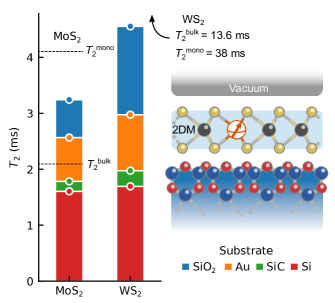
We start by discussing our results for the \chMoS_2 and \chWS_2 2DMs. In the absence of any interaction with the environment, Ye et al. [10] predicted that of a spin qubit in \chMoS_2 increases by a factor of 2 (, ms) when the nuclear bath of the host is reduced from 3D to 2D. The calculations of Ref.[10] neglected the quadrupole term in the spin Hamiltonian. When including such term, we found increased further ( ms), while the ratio between in 2D and 3D remains the same as previously reported. In natural \chWS_2, the nuclear bath contains a smaller number of nuclear spins than in \chMoS_2, with a relatively small gyromagnetic ratio. Hence the nuclear spin-induced decoherence in \chWS_2 is an order of magnitude slower than in \chMoS_2, and the increase in coherence time with reduced dimensionality becomes more significant: ms, 3 times higher than ms.
Next, we investigate how coherence times vary when \chMoS_2 and \chWS_2 are deposited on a substrate. We consider Au (111), Si (111) and \chSiO_2 (ideal siloxane-terminated surface) [38, 39, 40, 41]. These substrates have been used in spectroscopic measurements [39], and applications of 2DMs in catalysis[38, 40] and electronics [41]. We neglect the reconstruction of the surface of the substrate and we assume that the quadrupole couplings are the same as those of the pristine material in vacuum.
Under an applied magnetic field, the contributions to coherence times of the different species of the nuclear bath are decoupled [25]; hence:
| (2) |
where and are the contributions of the substrate (S) and of the 2DM host, respectively. We find that the nuclear baths of both the 2DM and the substrate may act as limiting factors to the qubit coherence. In particular, in \chWS_2 the qubit dynamics is completely determined by the substrate nuclear bath, and is significantly smaller than the one of the qubits in bulk \chWS_2 (Fig. 1). The coherence time depends on the nature of the substrate. The longest and shortest coherence times are obtained for \chSiO_2 and the Si (111) surface, respectively. These results can be understood by noticing that the Si substrate has the highest concentrations of \ch^29Si spins, compared to \chSiO_2 and \chSiC; the latter exhibits however an additional source of decoherence given by the \ch^13C bath. We also note that while gold contains the highest concentration of nuclear spins (100% \ch^197Au with ), the small gyromagnetic ratio and large separation of the nuclei lead to a moderate influence of the substrate on the coherence time of the 2D material, with ms.
In \chMoS_2, on the other hand, both the substrate and host contribute significantly to the qubit decoherence. We find that an enhancement of T2 from the reduced dimensionality persists only for the \chSiO_2 and gold substrates. In the presence of a Si (111) surface, the of a qubit in \chMoS_2 and \chWS_2 is almost identical.
We note that the presence of paramagnetic defects both on the surface of the substrate and in the 2DM itself may significantly impact decoherence rates and limit the value of . To decrease the number of paramagnetic impurities in the 2D host, advanced experimental techniques are being developed [42]. In general, to eliminate surface charges, it is desirable to reduce interfacial reconstructions as much as possible, and one way to achieve this objective is the use of van-der-Waals bonded materials as substrates. [43, 42].
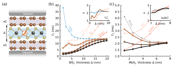
Hence we turn to consider heterostructures of van-der-Waals bonded materials, which are emerging as promising platforms for 2D-based photonics. For example, a heterostructure of layered graphene and \chWS_2 was recently used to realize atomic defect-based photon emitters [44]. To simulate the qubit dynamics in van-der-Waals bonded integrated systems, we focus on layered heterostructures with the spin qubit located in an inner layer, as shown in Fig. 2a.
We investigated the effect of the decoherence arising from the presence of a substrate (outer layer) and from the host (inner layer) of thickness ; the coherence time is obtained by fitting the coherence function contribution (Eq. 2) to the compressed exponential function, , where denotes either the substrate (S) or the host 2DM. We found that as increases, the rate of the decoherence induced by the host bath increases (see Fig. 2(b) and Fig. 2(c) for \chWS_2 and \chMoS_2, respectively). Instead the decoherence rate originating from the substrate nuclear bath decreases with the distance of the qubit from the substrate (see Fig. 2a and 2b, where C denotes the number of Carbon layers). The combination of these two factors may result in a non-monotonic behavior of the total coherence time of the heterostructure as a function of .
Fig. 2(b) shows our results for C/\chWS_2/C heterostructures. For nm, the effect of the substrate completely supersedes the effect of the host nuclear bath. With increasing , decreases, but increases. We find that for nm, is proportional to , where depends on the thickness of the outer layer; in particular for bulk graphite and for graphene. The interplay between the host- and substrate-induced decoherence leads to the appearance of a local maximum in the coherence time. When the thicknesses of the host material exceeds nm, the decoherence is essentially limited by that of the \chWS_2 bath.
Our results show that depending on the number of graphite layers in the substrate, the coherence time of monolayer \chMoS_2-based qubits can be either smaller or larger than in bulk \chMoS_2 (Fig 2(c)). The presence of two similar sources of decoherence arising from the host and the graphite/3C substrates leads to a minimum of the total coherence time around 4 nm.
As the distance from the graphite substrate increases, the nature of the substrate-induced decoherence process changes. In particular, the graphene-induced decoherence as a function of exhibits the most complex behavior: we observe a transition from a Gaussian () to an exponential decay () of the coherence function, near the local maximum in and in of the C/\chWS_2/C heterostructure. For large , approaches 3 for both graphene and bulk graphite environments (insets of Fig. 2b and c).
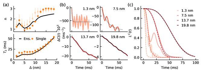
Fig. 3 shows the decoherence induced by graphene monolayers in ensemble dynamics and for individual bath configurations. Our calculations show that the ensemble-averaged decay induced by the graphene nuclear bath has a smaller compressed exponent than the mean of the individual fitted decays (Fig. 3(a)), consistent with the predictions of stochastic noise models[45, 46]. However, we find that of the ensemble is not reduced by a factor of two, but only by . Both ensemble and single spin dynamics show a non-monotonic variation of the coherence time with increased distance from the graphene substrate. We analyze below in detail the noise regimes of the Hahn-echo decay depending on the host thickness.
For nm, the dipolar coupling between nuclear spins in graphene is larger than the coupling of the graphene layer to the central spin. In this case, it is reasonable to assume that the Hahn-echo decay is governed by a classical Gaussian noise, and hence by the Hamiltonian:
| (3) |
where is the spin operator of the qubit electron spin, and changes its sign each time a pulse is applied [47]. is a stochastic variable, corresponding to the magnetic noise. Then the coherence function can be computed as [48]:
| (4) |
Where is the correlation of the Overhauser field of the nuclear bath. is a correlation filter function, defined as [48]:
| (5) |
We compute the noise correlation function with the CCE method [47, 49] from the autocorrelation function of the Overhauser field operator where is hyperfine coupling. The correlation function for one random nuclear spin configuration is shown in Fig. 3(b) for different separations of graphene layers from the qubit. The dotted black lines show the exponential fit , where is the correlation time of the bath. We observe that increases with thickness from 1.2 ms to 150 ms for the largest separation considered here. The long correlation time at large and the coherence decay of agree well with stochastic model predictions for the slow evolution of the bath[50, 51].
We further observe the emergence of a classical regime by reconstructing the coherence function from the noise correlation using Eq. 4 (Fig. 3(c)). We find that the semiclassical approach faithfully reproduces the complete quantum mechanical evolution of the bath at separations between graphene layers larger than 10 nm.
For 10 nm, however, the hyperfine coupling is on a par or significantly larger than the average dipolar coupling between nuclear spins, and a classical treatment of the noise is no longer appropriate[19]. In this case, a complex decay of the coherence function is observed (Fig. 3c), which is not captured by Eq. 4.
An insight into this complex dynamics can be gained by analyzing the evolution of a single pair of spins and . At sufficiently strong magnetic fields, only pairwise spin flip-flops are allowed (), and their dynamics can be mapped on a 2-level "pseudospin", governed by the Hamiltonian:
| (6) |
where the frequency of the pseudospin, , is given by the difference in hyperfine coupling, if the central spin is in the state, or if the central spin is in the state. are Pauli matrices for spin-. is obtained from the dipolar coupling of nuclear spins, where is the angle between the vector connecting two nuclear spins and the external magnetic field.
The total coherence function can be obtained analytically [52, 25] as a product of the contributions of all spin pairs :
| (7) |
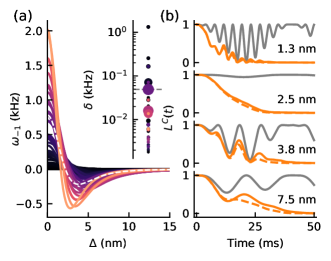
where . Due to the reduced dimensionality of graphene and the sparse concentration of nuclear spins, only a small number of spin pairs exists in close proximity of the qubit and thus contributes to determining the coherence decay. (Fig. 4).
The dependence of on the distance from the graphene layer can be computed from the hyperfine couplings of nuclear spins and is quite complex (Fig. 4(a)). As increases, the frequency of pseudospins changes its sign and exhibits a local extremum. At , the hyperfine couplings of two nuclear spins are the same, and the contribution of the spin pair to the coherence function becomes negligible (Fig. 4(b)). When the amplitude reaches a local maximum, the spin pair’s dynamics again significantly impacts the coherence function.
This unique behavior of the hyperfine couplings determines the non-monotonic dependence of and of the compressed exponent on the distance between the graphene layers and the qubit. We note the good agreement between the pseudospin prediction and the exact solution at small distances. For large values of , the pseudospin model gives an underestimation of the coherence time, due to the longer correlation time and to higher-order effects playing a dominant role.
Finally, we note that there are cases in which the choice of the substrate in van-der-Waals structures can completely suppress the effect of the host at any host thickness of interest. As an example, we consider h-BN as a substrate, whose nuclear spin bath contains 100% concentration of spins with a high gyromagnetic ratio. Using CCE calculations up to the second order, without quadrupole tensors included, we estimated the thickness of the qubit host at which the coherence time is determined purely by the host spin bath. We found a lower bound of nm for \chMoS_2 and nm for \chWS_2, respectively.
In sum, we presented a theoretical study of the influence of the environment on the coherence time of spin qubits in 2D materials. We found that both the nuclear spins of the substrate and those of the host 2DM can act as sources of decoherence for the qubit. Our results show that the composition of van-der-Waals heterostructures encapsulating the qubit may be engineered to obtain longer coherence times.
Our calculations also revealed a complex behavior of the Hahn-echo coherence time as a function of the thickness of the 2D material hosting the qubit. For thin hosts ( nm) it is possible to identify specifically which pairs of spins give rise to the oscillations observed in the Hahn-echo decay time. This result points at the possibility of using the electron spin of the qubit as a sensor of dipolar couplings within the 2D nuclear bath[53]. For thicker hosts ( nm), we observed a transition from a quantum to a classical regime of the induced decoherence, which might be revealed experimentally by using. e.g. a NV center in diamond as a quantum sensor[54, 55].
Finally we note that for the 2DMs investigated here, other decoherence channels (spin-orbit, spin-phonon interactions [56, 57, 58]) exist, which may play a significant role at nonzero temperatures. Their contribution to decoherence needs to be carefully assessed in the future. And although we focused only on the interaction of the spin defect with the nuclear spin bath, our results point at the importance of the substrate and its composition in the design of 2DMs and van-der-Waals heterostructures for quantum applications.
Acknowledgements
This work made use of resources provided by the University of Chicago’s Research Computing Center. This work was supported as part of the Center for Novel Pathways to Quantum Coherence in Materials, an Energy Frontier Research Center funded by the U.S. Department of Energy, Office of Science, Basic Energy Sciences. We thank Meng Ye, Yuxin Wang, and Siddhartha Sohoni for useful discussions.
Data Availability
The data that support the findings of this study are available from the corresponding author upon reasonable request.
References
- Liu and Hersam [2019] X. Liu and M. C. Hersam, “2d materials for quantum information science,” Nature Reviews Materials 4, 669–684 (2019).
- Fuchs, Rychkov, and Trauzettel [2012] M. Fuchs, V. Rychkov, and B. Trauzettel, “Spin decoherence in graphene quantum dots due to hyperfine interaction,” Phys. Rev. B 86, 085301 (2012).
- Volk et al. [2013] C. Volk, C. Neumann, S. Kazarski, S. Fringes, S. Engels, F. Haupt, A. Müller, and C. Stampfer, “Probing relaxation times in graphene quantum dots,” Nature Communications 4, 1753 (2013).
- Chejanovsky et al. [2016] N. Chejanovsky, M. Rezai, F. Paolucci, Y. Kim, T. Rendler, W. Rouabeh, F. Fávaro de Oliveira, P. Herlinger, A. Denisenko, S. Yang, I. Gerhardt, A. Finkler, J. H. Smet, and J. Wrachtrup, “Structural attributes and photodynamics of visible spectrum quantum emitters in hexagonal boron nitride,” Nano Letters 16, 7037–7045 (2016).
- Koperski et al. [2015] M. Koperski, K. Nogajewski, A. Arora, V. Cherkez, P. Mallet, J.-Y. Veuillen, J. Marcus, P. Kossacki, and M. Potemski, “Single photon emitters in exfoliated wse2 structures,” Nature Nanotechnology 10, 503–506 (2015).
- Barthelmi et al. [2020] K. Barthelmi, J. Klein, A. Hötger, L. Sigl, F. Sigger, E. Mitterreiter, S. Rey, S. Gyger, M. Lorke, M. Florian, F. Jahnke, T. Taniguchi, K. Watanabe, V. Zwiller, K. D. Jöns, U. Wurstbauer, C. Kastl, A. Weber-Bargioni, J. J. Finley, K. Müller, and A. W. Holleitner, “Atomistic defects as single-photon emitters in atomically thin mos2,” Applied Physics Letters 117, 070501 (2020), https://doi.org/10.1063/5.0018557 .
- Exarhos et al. [2019] A. L. Exarhos, D. A. Hopper, R. N. Patel, M. W. Doherty, and L. C. Bassett, “Magnetic-field-dependent quantum emission in hexagonal boron nitride at room temperature,” Nature Communications 10, 222 (2019).
- Gottscholl et al. [2020a] A. Gottscholl, M. Kianinia, V. Soltamov, S. Orlinskii, G. Mamin, C. Bradac, C. Kasper, K. Krambrock, A. Sperlich, M. Toth, I. Aharonovich, and V. Dyakonov, “Initialization and read-out of intrinsic spin defects in a van der waals crystal at room temperature,” Nature Materials 19, 540–545 (2020a).
- Gottscholl et al. [2020b] A. Gottscholl, M. Diez, V. Soltamov, C. Kasper, A. Sperlich, M. Kianinia, C. Bradac, I. Aharonovich, and V. Dyakonov, “Room temperature coherent control of spin defects in hexagonal boron nitride,” (2020b), arXiv:2010.12513 [cond-mat.mes-hall] .
- Ye, Seo, and Galli [2019] M. Ye, H. Seo, and G. Galli, “Spin coherence in two-dimensional materials,” npj Computational Materials 5, 44 (2019).
- McCreary et al. [2016] K. M. McCreary, A. T. Hanbicki, S. Singh, R. K. Kawakami, G. G. Jernigan, M. Ishigami, A. Ng, T. H. Brintlinger, R. M. Stroud, and B. T. Jonker, “The effect of preparation conditions on raman and photoluminescence of monolayer ws2,” Scientific Reports 6, 35154 (2016).
- Shin et al. [2016] B. G. Shin, G. H. Han, S. J. Yun, H. M. Oh, J. J. Bae, Y. J. Song, C.-Y. Park, and Y. H. Lee, “Indirect bandgap puddles in monolayer mos2 by substrate-induced local strain,” Advanced Materials 28, 9378–9384 (2016), https://onlinelibrary.wiley.com/doi/pdf/10.1002/adma.201602626 .
- Fiori et al. [2014] G. Fiori, F. Bonaccorso, G. Iannaccone, T. Palacios, D. Neumaier, A. Seabaugh, S. K. Banerjee, and L. Colombo, “Electronics based on two-dimensional materials,” Nature Nanotechnology 9, 768–779 (2014).
- Lee et al. [2020] E. Lee, S. G. Lee, W. H. Lee, H. C. Lee, N. N. Nguyen, M. S. Yoo, and K. Cho, “Direct cvd growth of a graphene/mos2 heterostructure with interfacial bonding for two-dimensional electronics,” Chemistry of Materials 32, 4544–4552 (2020).
- Britnell et al. [2012] L. Britnell, R. V. Gorbachev, R. Jalil, B. D. Belle, F. Schedin, A. Mishchenko, T. Georgiou, M. I. Katsnelson, L. Eaves, S. V. Morozov, N. M. R. Peres, J. Leist, A. K. Geim, K. S. Novoselov, and L. A. Ponomarenko, “Field-effect tunneling transistor based on vertical graphene heterostructures,” Science 335, 947–950 (2012), https://science.sciencemag.org/content/335/6071/947.full.pdf .
- Bertolazzi, Krasnozhon, and Kis [2013] S. Bertolazzi, D. Krasnozhon, and A. Kis, “Nonvolatile memory cells based on mos2/graphene heterostructures,” ACS Nano 7, 3246–3252 (2013).
- Choi et al. [2017] W. Choi, N. Choudhary, G. H. Han, J. Park, D. Akinwande, and Y. H. Lee, “Recent development of two-dimensional transition metal dichalcogenides and their applications,” Materials Today 20, 116 – 130 (2017).
- Aharonovich, Englund, and Toth [2016] I. Aharonovich, D. Englund, and M. Toth, “Solid-state single-photon emitters,” Nature Photonics 10, 631–641 (2016).
- Yang, Ma, and Liu [2016] W. Yang, W.-L. Ma, and R.-B. Liu, “Quantum many-body theory for electron spin decoherence in nanoscale nuclear spin baths,” Reports on Progress in Physics 80, 016001 (2016).
- Chirolli and Burkard [2008] L. Chirolli and G. Burkard, “Decoherence in solid-state qubits,” Advances in Physics 57, 225–285 (2008), https://doi.org/10.1080/00018730802218067 .
- Yang and Liu [2008] W. Yang and R.-B. Liu, “Quantum many-body theory of qubit decoherence in a finite-size spin bath,” Phys. Rev. B 78, 085315 (2008).
- Yang and Liu [2009] W. Yang and R.-B. Liu, “Quantum many-body theory of qubit decoherence in a finite-size spin bath. ii. ensemble dynamics,” Phys. Rev. B 79, 115320 (2009).
- Ma et al. [2014] W.-L. Ma, G. Wolfowicz, N. Zhao, S.-S. Li, J. J. Morton, and R.-B. Liu, “Uncovering many-body correlations in nanoscale nuclear spin baths by central spin decoherence,” Nature Communications 5, 4822 (2014).
- Balian et al. [2014] S. J. Balian, G. Wolfowicz, J. J. L. Morton, and T. S. Monteiro, “Quantum-bath-driven decoherence of mixed spin systems,” Phys. Rev. B 89, 045403 (2014).
- Seo et al. [2016] H. Seo, A. L. Falk, P. V. Klimov, K. C. Miao, G. Galli, and D. D. Awschalom, “Quantum decoherence dynamics of divacancy spins in silicon carbide,” Nature Communications 7, 12935 (2016).
- Onizhuk et al. [2021] M. Onizhuk, K. C. Miao, J. P. Blanton, H. Ma, C. P. Anderson, A. Bourassa, D. D. Awschalom, and G. Galli, “Probing the coherence of solid-state qubits at avoided crossings,” PRX Quantum 2, 010311 (2021).
- Lin et al. [2016] Z. Lin, B. R. Carvalho, E. Kahn, R. Lv, R. Rao, H. Terrones, M. A. Pimenta, and M. Terrones, “Defect engineering of two-dimensional transition metal dichalcogenides,” 2D Materials 3, 022002 (2016).
- Kennedy et al. [2003] T. A. Kennedy, J. S. Colton, J. E. Butler, R. C. Linares, and P. J. Doering, “Long coherence times at 300 k for nitrogen-vacancy center spins in diamond grown by chemical vapor deposition,” Applied Physics Letters 83, 4190–4192 (2003), https://doi.org/10.1063/1.1626791 .
- Bourassa et al. [2020] A. Bourassa, C. P. Anderson, K. C. Miao, M. Onizhuk, H. Ma, A. L. Crook, H. Abe, J. Ul-Hassan, T. Ohshima, N. T. Son, G. Galli, and D. D. Awschalom, “Entanglement and control of single nuclear spins in isotopically engineered silicon carbide,” Nature Materials (2020), 10.1038/s41563-020-00802-6.
- Perdew, Burke, and Ernzerhof [1996] J. P. Perdew, K. Burke, and M. Ernzerhof, “Generalized gradient approximation made simple,” Phys. Rev. Lett. 77, 3865–3868 (1996).
- [31] https://github.com/dceresoli/qe-gipaw, accessed: Jul. 14, 2020.
- Giannozzi et al. [2009] P. Giannozzi, S. Baroni, N. Bonini, M. Calandra, R. Car, C. Cavazzoni, D. Ceresoli, G. L. Chiarotti, M. Cococcioni, I. Dabo, A. D. Corso, S. de Gironcoli, S. Fabris, G. Fratesi, R. Gebauer, U. Gerstmann, C. Gougoussis, A. Kokalj, M. Lazzeri, L. Martin-Samos, N. Marzari, F. Mauri, R. Mazzarello, S. Paolini, A. Pasquarello, L. Paulatto, C. Sbraccia, S. Scandolo, G. Sclauzero, A. P. Seitsonen, A. Smogunov, P. Umari, and R. M. Wentzcovitch, “Quantum espresso: a modular and open-source software project for quantum simulations of materials,” J. Phys.: Condens. Matter 21, 395502 (2009).
- Velický et al. [2018] M. Velický, G. E. Donnelly, W. R. Hendren, S. McFarland, D. Scullion, W. J. I. DeBenedetti, G. C. Correa, Y. Han, A. J. Wain, M. A. Hines, D. A. Muller, K. S. Novoselov, H. D. Abruña, R. M. Bowman, E. J. G. Santos, and F. Huang, “Mechanism of gold-assisted exfoliation of centimeter-sized transition-metal dichalcogenide monolayers,” ACS Nano 12, 10463–10472 (2018).
- Dolui, Rungger, and Sanvito [2013] K. Dolui, I. Rungger, and S. Sanvito, “Origin of the -type and -type conductivity of mos2 monolayers on a sio2 substrate,” Phys. Rev. B 87, 165402 (2013).
- Wang et al. [2019] Y. Wang, J. C. Kim, R. J. Wu, J. Martinez, X. Song, J. Yang, F. Zhao, A. Mkhoyan, H. Y. Jeong, and M. Chhowalla, “Van der waals contacts between three-dimensional metals and two-dimensional semiconductors,” Nature 568, 70–74 (2019).
- Zhang et al. [2017] F. Zhang, W. Li, Y. Ma, Y. Tang, and X. Dai, “Tuning the schottky contacts at the graphene/ws2 interface by electric field,” RSC Adv. 7, 29350–29356 (2017).
- Wang, Chen, and Wang [2015] Z. Wang, Q. Chen, and J. Wang, “Electronic structure of twisted bilayers of graphene/mos2 and mos2/mos2,” The Journal of Physical Chemistry C 119, 4752–4758 (2015).
- Shi et al. [2014] J. Shi, D. Ma, G.-F. Han, Y. Zhang, Q. Ji, T. Gao, J. Sun, X. Song, C. Li, Y. Zhang, X.-Y. Lang, Y. Zhang, and Z. Liu, “Controllable growth and transfer of monolayer mos2 on au foils and its potential application in hydrogen evolution reaction,” ACS Nano 8, 10196–10204 (2014).
- Wood et al. [2020] R. E. Wood, L. T. Lloyd, F. Mujid, L. Wang, M. A. Allodi, H. Gao, R. Mazuski, P.-C. Ting, S. Xie, J. Park, and G. S. Engel, “Evidence for the dominance of carrier-induced band gap renormalization over biexciton formation in cryogenic ultrafast experiments on mos2 monolayers,” The Journal of Physical Chemistry Letters 11, 2658–2666 (2020).
- Shi et al. [2016] J. Shi, R. Tong, X. Zhou, Y. Gong, Z. Zhang, Q. Ji, Y. Zhang, Q. Fang, L. Gu, X. Wang, Z. Liu, and Y. Zhang, “Temperature-mediated selective growth of mos2/ws2 and ws2/mos2 vertical stacks on au foils for direct photocatalytic applications,” Advanced Materials 28, 10664–10672 (2016), https://onlinelibrary.wiley.com/doi/pdf/10.1002/adma.201603174 .
- Hasani et al. [2019] A. Hasani, Q. Van Le, M. Tekalgne, M.-J. Choi, S. Choi, T. H. Lee, H. Kim, S. H. Ahn, H. W. Jang, and S. Y. Kim, “Fabrication of a ws2/p-si heterostructure photocathode using direct hybrid thermolysis,” ACS Applied Materials & Interfaces 11, 29910–29916 (2019).
- Rhodes et al. [2019] D. Rhodes, S. H. Chae, R. Ribeiro-Palau, and J. Hone, “Disorder in van der waals heterostructures of 2d materials,” Nature Materials 18, 541–549 (2019).
- Pisoni et al. [2018] R. Pisoni, A. Kormányos, M. Brooks, Z. Lei, P. Back, M. Eich, H. Overweg, Y. Lee, P. Rickhaus, K. Watanabe, T. Taniguchi, A. Imamoglu, G. Burkard, T. Ihn, and K. Ensslin, “Interactions and magnetotransport through spin-valley coupled landau levels in monolayer ,” Phys. Rev. Lett. 121, 247701 (2018).
- Schuler et al. [2020] B. Schuler, K. A. Cochrane, C. Kastl, E. S. Barnard, E. Wong, N. J. Borys, A. M. Schwartzberg, D. F. Ogletree, F. J. G. de Abajo, and A. Weber-Bargioni, “Electrically driven photon emission from individual atomic defects in monolayer ws2,” Science Advances 6 (2020), 10.1126/sciadv.abb5988, https://advances.sciencemag.org/content/6/38/eabb5988.full.pdf .
- Bauch et al. [2020] E. Bauch, S. Singh, J. Lee, C. A. Hart, J. M. Schloss, M. J. Turner, J. F. Barry, L. M. Pham, N. Bar-Gill, S. F. Yelin, and R. L. Walsworth, “Decoherence of ensembles of nitrogen-vacancy centers in diamond,” Phys. Rev. B 102, 134210 (2020).
- Dobrovitski et al. [2008] V. V. Dobrovitski, A. E. Feiguin, D. D. Awschalom, and R. Hanson, “Decoherence dynamics of a single spin versus spin ensemble,” Phys. Rev. B 77, 245212 (2008).
- Witzel, Young, and Das Sarma [2014] W. M. Witzel, K. Young, and S. Das Sarma, “Converting a real quantum spin bath to an effective classical noise acting on a central spin,” Phys. Rev. B 90, 115431 (2014).
- Young and Whaley [2012] K. C. Young and K. B. Whaley, “Qubits as spectrometers of dephasing noise,” Phys. Rev. A 86, 012314 (2012).
- Ma et al. [2015] W.-L. Ma, G. Wolfowicz, S.-S. Li, J. J. L. Morton, and R.-B. Liu, “Classical nature of nuclear spin noise near clock transitions of bi donors in silicon,” Phys. Rev. B 92, 161403 (2015).
- Klauder and Anderson [1962] J. R. Klauder and P. W. Anderson, “Spectral diffusion decay in spin resonance experiments,” Phys. Rev. 125, 912–932 (1962).
- de Sousa and Das Sarma [2003] R. de Sousa and S. Das Sarma, “Electron spin coherence in semiconductors: Considerations for a spin-based solid-state quantum computer architecture,” Phys. Rev. B 67, 033301 (2003).
- Yao, Liu, and Sham [2006] W. Yao, R.-B. Liu, and L. J. Sham, “Theory of electron spin decoherence by interacting nuclear spins in a quantum dot,” Phys. Rev. B 74, 195301 (2006).
- Abobeih et al. [2019] M. H. Abobeih, J. Randall, C. E. Bradley, H. P. Bartling, M. A. Bakker, M. J. Degen, M. Markham, D. J. Twitchen, and T. H. Taminiau, “Atomic-scale imaging of a 27-nuclear-spin cluster using a quantum sensor,” Nature 576, 411–415 (2019).
- Lovchinsky et al. [2017] I. Lovchinsky, J. D. Sanchez-Yamagishi, E. K. Urbach, S. Choi, S. Fang, T. I. Andersen, K. Watanabe, T. Taniguchi, A. Bylinskii, E. Kaxiras, P. Kim, H. Park, and M. D. Lukin, “Magnetic resonance spectroscopy of an atomically thin material using a single-spin qubit,” Science 355, 503–507 (2017), https://science.sciencemag.org/content/355/6324/503.full.pdf .
- Zhou et al. [2020] B. B. Zhou, P. C. Jerger, K.-H. Lee, M. Fukami, F. Mujid, J. Park, and D. D. Awschalom, “Spatiotemporal mapping of a photocurrent vortex in monolayer using diamond quantum sensors,” Phys. Rev. X 10, 011003 (2020).
- Xu et al. [2020] J. Xu, A. Habib, S. Kumar, F. Wu, R. Sundararaman, and Y. Ping, “Spin-phonon relaxation from a universal ab initio density-matrix approach,” Nature Communications 11, 2780 (2020).
- Wang et al. [2015] Z. Wang, D.-K. Ki, H. Chen, H. Berger, A. H. MacDonald, and A. F. Morpurgo, “Strong interface-induced spin–orbit interaction in graphene on ws2,” Nature Communications 6, 8339 (2015).
- Yang et al. [2015] L. Yang, N. A. Sinitsyn, W. Chen, J. Yuan, J. Zhang, J. Lou, and S. A. Crooker, “Long-lived nanosecond spin relaxation and spin coherence of electrons in monolayer mos2 and ws2,” Nature Physics 11, 830–834 (2015).