Metal-insulator transition in -type bulk crystals and films of strongly compensated SrTiO3
Abstract
We start by analyzing experimental data of Spinelli et al Spinelli et al. (2010) for the conductivity of -type bulk crystals of SrTiO3 (STO) with broad electron concentration range of - cm-3, at low temperatures. We obtain good fit of the conductivity data, , by the Drude formula for cm-3 assuming that used for doping insulating STO bulk crystals are strongly compensated and the total concentration of background charged impurities is cm-3. At , the conductivity collapses with decreasing and the Drude theory fit fails. We argue that this is the metal-insulator transition (MIT) in spite of the very large Bohr radius of hydrogen-like donor state nm with which the Mott criterion of MIT for a weakly compensated semiconductor, , predicts times smaller . We try to explain this discrepancy in the framework of the theory of the percolation MIT in a strongly compensated semiconductor with the same cm-3. In the second part of this paper, we develop the percolation MIT theory for films of strongly compensated semiconductors. We apply this theory to doped STO films with thickness nm and calculate the critical MIT concentration . We find that, for doped STO films on insulating STO bulk crystals, grows with decreasing . Remarkably, STO films in a low dielectric constant environment have the same . This happens due to the Rytova-Keldysh modification of a charge impurity potential which allows a larger number of the film charged impurities to contribute to the random potential.
I Introduction
SrTiO3 (STO) is a classic example of perovskite oxides. Historically, the primary interest in this material was on its unusual dielectric properties. The dielectric constant increases from around 300 at K to 20000 at low temperatures. Due to its widespread use as a single-crystal substrate for epitaxial growth of oxides, its commercial availability, controllable surface termination, and close lattice match to numerous complex oxide materials, STO has been employed as an active component in oxide heterostructures and thin films. Examples include, its use as a dielectric layer in field-effect devices for tuning the carrier density of materials such as cuprates, and in such systems as forming a two-dimensional electron gas interface.
In this paper, we are concerned with fascinating and potentially useful, electronic transport properties of STO, which is a semiconductor with a 3.2 eV gap. -type conduction of STO has been most commonly achieved by substitution of for , for , or by oxygen reduction to . Similarly, -type doping has been achieved by substituting trivalent metal ions, such as , , , and for . Transport data for electron doped STO bulk crystals are summarized in Ref. Spinelli et al. (2010). Within the hydrogenic theory of shallow donors, the donor Bohr radius, nm, where Uwe et al. (1985); Allen et al. (2013) is the effective electron mass and is free electron mass. At K, nm is so large that the Mott criterion for the metal-insulator transition (MIT) in doped weakly compensated semiconductors Mott (1969), , leads to a very small cm-3. Thus, at all experimental concentrations of donors and electrons cm-3, STO should be strongly degenerate and should have metallic conductivity.
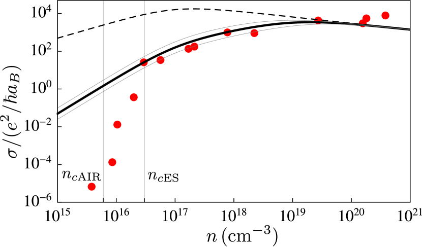
Reference Spinelli et al. (2010) presents temperature dependencies of resistivity for a large set of -type STO samples with electron concentrations ranging from to cm-3 . In Fig. 1, we plot by red dots the conductivity at 4 K obtained in Ref. Spinelli et al. (2010) as a function of . (All the lines at Fig. 1 are theoretical results and will be explained later). We see that the character of dependence of dramatically changes around cm-3. This apparent MIT at cm-3 is in dramatic contradiction with the theoretical prediction, based on the Mott criterion.
In this paper, we address this puzzle and show that the Mott criterion fails because insulating bulk crystals of STO used for intentional doping are almost completely compensated, i.e., have large and almost equal concentrations of background charged donors and acceptors. When the intentionally added concentration of donors and electrons is much smaller than , MIT is driven by the random long-range Coulomb potential of charged donors and acceptors Shklovskii and Efros (1971, 2013). With decreasing , the Fermi energy of degenerate electron gas gets smaller while the screening of Coulomb potential of impurities gets weaker. At some , the amplitude of potential fluctuations becomes larger than the depth of the electron Fermi sea and electrons get localized in large puddles separated from each other by large potential barriers. We call such a transition the percolation MIT in strongly compensated semiconductor, to discriminate it from the Mott MIT in weakly compensated semiconductor.
The plan of this paper is as follows. In Sec. II, we analyze the experimental data of Spinelli et al Spinelli et al. (2010) for conductivity at 4 K shown in Fig. 1. We calculate the Drude conductivity, , of compensated STO assuming that the scattering happens only on randomly positioned Coulomb impurities. For cm-3, we obtained reasonably good fit of the conductivity data, , with the concentration of background charged impurities cm-3. Using this , we show that the theory of the percolation MIT of Refs. Shklovskii and Efros (1971, 2013) gives close to the experimental value.
In Sec. III, we extend the percolation MIT theory to films of strongly compensated STO with thickness nm and calculate the critical MIT electron concentration . We find that grows with decreasing , because the Rytova-Keldysh modification of the Coulomb potential of a charge impurity slows down its potential decay within the STO film, and allows a larger number of the film impurities to contribute to the random potential breaking Fermi sea in puddles. The theory of the percolation MIT developed here for STO films is valid for all other compensated semiconductor films.
II Conductivity and metal-insulator transition in STO bulk crystals.
Let us start from the low temperature theory of metallic conductivity. At large , when , electron gas is degenerate and , where is the Fermi wave vector and is the mean free path, so that one can use the Drude formula for conductivity: , where is the momentum relaxation time, is the Fermi velocity, and is the charge of an electron. At low temperatures the dominant scattering mechanism is due to ionized donors. In the standard Thomas-Fermi approximation, the screening radius of the degenerate electron gas Mott (1936); Mansfield (1956) is much larger than the electron wavelength, , so one can use the screened Coulomb potential to compute the momentum relaxation time and the corresponding conductivity. Under the assumption that compensation is absent and the number of ionized impurity centers is the same as the number of free carriers, , we get for the conductivity of a degenerate gas
| (1) |
where .
Due to the large dielectric constant, the scattering cross section, , used to calculate Eq. (1), gets very small quickly, as increases. For cm-3, , where is the lattice constant for STO. Following Ref. Wemple (1965), we argue that once , it saturates and can not get any smaller with increasing . Indeed, for length scales of the order , there is no more dielectric screening, so the electron “feels” the full potential of the charged impurity center . It leads to the geometrical cross section of the donor of the order of . As a result, for cm-3, Eq. (1) is no longer valid and the conductivity is given by
| (2) |
We see from Eq. (2) that decreases with increasing as . This dependence was first derived in Refs. Morita, 1963; Shimizu, 1963 and observed in heavily doped PbTe and SnTe in Ref. Allgaier and Houston, 1962. Using the Matthiessen addition rule, , to interpolate between Eqs. (1) and (2), we plot the dimensionless conductivity versus the carriers concentration in Fig. 1 by the dashed line. We see that at relatively small such ignoring compensation theory predicts 2-3 orders of magnitude larger conductivity than the data.
We argue that the experimental conductivity is small because of almost complete compensation of insulating STO crystals used in Ref. Spinelli et al., 2010 and universally for intentional doping by donors. Namely, these insulating samples contain uncontrolled and practically equal concentrations of background donors () and acceptors () Tufte and Chapman (1967); Spinelli et al. (2010); Ambwani et al. (2016). Thus, the total concentration of charged impurities is large and this strongly reduces the conductivity. Below, we present an evidence that cm-3.
Background impurities increase the total number of Coulomb impurities to , and replace Eqs. (1) and (2) by the following two equations:
| (3) | ||||
| (4) |
We found that conductivity of a strongly compensated sample interpolated between Eqs. (3) and (4) gives the best fit to the experimental data. This fit is shown in Fig. 1 by the thick black line at cm-3, which agrees much better with the data than the dashed line obtained for uncompensated samples. However, for larger , while theory predicts that conductivity should go down with as , the experiment shows that it saturates or even slightly (like ) grows. This remains an unsolved puzzle 111In the recent paper Verma et al. (2014) the authors used an unrealistic parameters such as instead of and the effective mass instead of in order to fit data of Ref. Cain et al. (2013). In this way they were able to get inequality , which allowed them to use theory of Ref. Frederikse and Hosler (1967) to predict a saturating behavior for conductivity at large and avoid dealing with compensation. However, as the authors admit there is no justification for using such parameters. In reality, and the theory Mott (1936); Mansfield (1956) is applicable..
Mott’s condition for MIT critical concentration, , was derived for weakly compensated samples, so it is understandable that it does not predict the correct critical concentration for strongly compensated samples. To include the effect of compensation one can try the Anderson-Ioffe-Regel (AIR) condition for MITAnderson (1958); Ioffe and Regel (1960). The mean free path of charge carriers in a strongly compensated STO sample with is
| (5) |
Assuming that cm-3, we find the critical concentration for MIT to be cm-3. However, as shown in Fig. 1, the predicted is still five times smaller than experimental . To understand such discrepancy, notice that the Anderson-Ioffe-Regel MIT criterion is justified for scattering by individual random charges calculated in Born approximation. However, Efros and Shklovskii Shklovskii and Efros (1971, 2013) showed that the physics of strongly compensated semiconductor is dominated by large long range Coulomb potential of large number of charged impurities which, because of week screening at MIT, becomes larger than the Fermi energy of electrons and, therefore, breaks the electron gas in puddles separated by potential barriers at . Clearly, such situation can not be dealt with in Born approximation. This transition happens while locally, in puddles, electron gas is still a good metal with . This means that . Predicted Shklovskii and Efros (1971, 2013) is given by
| (6) |
where is a numerical coefficient. Analysis of experiments in compensated germanium shows Shklovskii and Efros (2013) that . Using cm-3, we find that cm-3. We see from the Fig. 1 that for strongly compensated semiconductor this critical concentration agrees much better with experimental MIT than . As we mentioned in Introduction the Mott criterion for weakly compensated semiconductor (where it is equivalent to AIR), , is more than times off.
The derivation of Eq. (6) is very simple Shklovskii and Efros (1971, 2013). One estimates the amplitude of fluctuations of the bottom of conduction band in electrostatic potential fluctuations in a good metal with randomly distributed Coulomb impurities, where is the screening radius for a degenerate electron gas. Then, one equates to the Fermi energy and solves for .
Although Eq. (6) agrees with apparent MIT at cm-3 our theory meets two big problems when compared to the data Spinelli et al. (2010).
First, one should recall that this is a zero temperature theory. It can work at finite temperature only if at both the Fermi energy and the amplitude of disorder potential are larger than . In reality simple estimates show that at temperature 4 K they are four times smaller than . Thus, no transition and localization of electrons in puddles can happen at K. At , energy , it grows with decreasing , but quite slowly Shklovskii and Efros (1971, 2013). Even for the sample with cm-3 is still 2 times smaller than at K. How can this sample have ? This may happen only if the disorder potential is 30 times larger than our . We have no idea how to explain such apparent large energy scale of disorder. Even if we were able to do that, we would arrive much larger in disagreement with experimental data Spinelli et al. (2010).
Second, the resistivity of the sample with cm-3 measured down to K while being very large showed apparent metal-like saturation at low temperatures. This disagrees with expected in strongly compensated semiconductor low temperature variable range hopping conductivity Shklovskii (1973). We have no explanation for such behavior.
It was assumed above that donors and acceptors positions are random, i.e., they are not making compact donor-acceptor pairs. For samples made by cooling from a melt, the distribution of impurities in space is a snapshot of the distribution that impurities have at higher temperature, when their diffusion practically freezes Keldysh and Proshko (1963). In relatively narrow band gap semiconductors, at this temperature there is a concentration of intrinsic carriers larger than the concentration of impurities. Intrinsic carriers thus screen the Coulomb attraction between donor and acceptors, so that impurities remain randomly distributed in space. As a result, when the temperature is lowered to the point where intrinsic carriers recombine, the impurities are left in random positions Gal’pern and Efros (1972); Shklovskii and Efros (2013). STO is a wide gap semiconductor so that explanation based on intrinsic carriers does not work. However, at temperatures of diffusion freezing, say 1000 K, STO still has a very large dielectric constant . Therefore, acceptors and donors of strongly compensated STO can avoid making pairs 222We can use analogy with water solutions () of simple salt such as NaCl, where ions and play the role of our donors and acceptors. It is known that at K salt stays dissociated till concentrations as large as cm-3. Here we are dealing with similar , comparable to two hydration radii of ions in water minimum distance between donor and acceptor (lattice constant of STO), but larger and much smaller concentration cm-3. Thus, almost all donor-acceptor pairs should be dissociated at temperature of diffusion freezing in STO..
III Metal-insulator transition in STO films
STO films attract growing attention Kozuka et al. (2009, 2010); Verma et al. (2014); Ambwani et al. (2016); Liu et al. (2012). They are made by three different methods: molecular beam epitaxy (MBE), pulse laser deposition (PLD), and spattering. MBE films are grown from high purity elements and may have less impurities and are relatively clean. PLD films are often grown from STO single crystal targets and are presumed to have the same or close composition, i.e., they are strongly compensated and have approximately the same as STO bulk crystals. Spattered films are typically grown from polycrystalline bulk targets and have even more impurities Ambwani et al. (2016).
In this paper, we focus on PLD films. They can be intentionally doped by donors and studied in large range of concentration of electrons . In this section, we calculate the critical concentration of electrons at MIT as a function of the film thickness . We show below that because of very large dielectric constant of STO, the dielectric constant of the film environment dramatically affects the amplitude of the long range random potential of Coulomb impurities of the film and, therefore, the critical concentration of MIT . Here we consider two interesting experimental situations: -type doped STO film surrounded by materials with much smaller dielectric constant and doped STO thin film on insulating STO substrate.
III.1 STO film in low dielectric constant environment
In this section, we study thin STO films with dielectric constant in environment with dielectric constant , for example STO grown on (and capped with) a non-STO perovskite insulators with much lower dielectric constants . In this case, according to Rytova and Keldysh Rytova (1967); Keldysh (1979); Cudazzo et al. (2011), the electric field lines of a charged impurity channel through the thin film before exiting outside to the environment at distance . At , the potential of such impurity is only logarithmically different from . Electrons screen this potential at some screening radius . At MIT, the screening becomes nonlinear and can be estimated from the condition that fluctuations of impurity charge concentration in the volume can be barely compensated by the redistribution of the concentration of electrons , such that . This gives
| (7) |
The corresponding amplitude of the Coulomb potential energy fluctuations is
| (8) |
In order to estimate the critical concentration of the MIT, we equate the potential energy to the Fermi energy
| (9) |
To proceed further, we should relate the local Fermi wave vector with the local density . First, consider a very thin film such that the motion along the perpendicular to film direction is quantized and restricted to the lowest subband. Namely, the Fermi energy is smaller than the subband gap , or equivalently . In such a thin film, electrons have only two degrees of freedom parallel to the film plane, and . Substituting back into Eq. (9), we arrive at the critical concentration
| (10) |
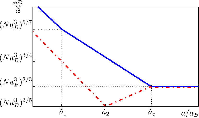
where is the effective STO Bohr radius. The above result is self-consistent if , which gives . For cm-3 and nm, we have nm.
Next, consider a thicker film with and . In this case, Eq. (9) gives the critical concentration
| (11) |
At , Eq. (11) crosses over to Eq. (10), while at , Eq. (11) matches the bulk value Eq. (6). For cm-3 and nm, we have nm. Eqs. (10), (11), and (6) are shown by the blue solid curve in Fig. 2.
Since the above results Eqs. (10) and (11) are based on , one should check if it as indeed satisfied near our MIT line. Inequality gives the restriction on
| (12) |
The upper and lower bounds on Eq. (12) cross the curve Eqs. (10) and (11) at and respectively. For typical , the lower limit nm. Thus, our phase boundary is valid at all reasonable film widths .
Above we ignored the concentration of charged impurities in the environment of the STO film, . Let us now evaluate the role of such impurities following similar analysis in the case of topological insulator films Huang and Shklovskii (2021). To save the electrostatic energy, the electric field lines of an impurity at distance from the film surface first enter inside the STO film and then radially spread inside the film to distance before exiting outside the film to infinity. Thus one can think that effectively each outside impurity is represented inside the film by a charge disk, with radius and thickness . In the presence of screening, only small minority of the outside impurities with contribute in fluctuating charge of the volume . As a result, total effective concentration of impurities projected from outside the film is . If , where is given by Eq. (7) at , outside impurities can be ignored and our results for are valid. Using Eqs. (10) and (11), we get at and at . We see that grows with decreasing , making small more vulnerable to external impurities. Thus, for , the condition of validity of above results is .
III.2 Doped STO film on the insulating STO substrate
In this case, the dielectric constant is uniform and we can deal with the conventional Coulomb potential of charged impurities with uniform concentration . At MIT, the screening by the electrons of doped STO film becomes nonlinear. The nonlinear screening radius can be estimated from the condition that fluctuations of the impurity charge concentration in the volume of a cube including a square of the STO film can be barely compensated by redistribution of the concentration of electrons inside the film Shklovskii and Efros (1986):
| (13) |
This gives
| (14) |
The corresponding amplitude of the Coulomb potential fluctuations therefore is
| (15) |
Remarkably, we arrive at the same result Eq. (8), as for doped STO films in a low dielectric constant environment. This means that for the case of a doped STO film on an insulating STO substrate, the phase boundary is identical to one given by Eqs. (10) and (11) and shown by the blue line of Fig. 2, which was originally derived for doped STO films in low dielectric constant free of impurities environment. It is remarkable that due to the Rytova-Keldysh effect, relatively small total number of impurities of the film lead to the same disorder effect as much larger number of impurities in the insulating STO substrate.
To emphasize importance of the Rytova-Keldysh effect, we briefly consider a case of doped STO film on relatively a thick buffer layer of undoped STO grown by MBE, which and concentration of impurities can be ignored. In this case, the amplitude of potential fluctuations 333In Eq. (16) a logarithmic factor is neglected, so the results Eqs. (17) and (18) are correct up to some logarithmic factors.
| (16) |
and is independent on the screening length . Next we estimate the critical concentration using similar to the previous section. If , then , and gives
| (17) |
where corresponds to . On the other hand, if , then , and gives
| (18) |
At , crosses over to the bulk value Eq. (6). For cm-3 and nm, nm. Equations. (17) and (18) are shown by the red dot-dashed curve in Fig. 2, which at is substantially lower than the blue curve. Thus we see that the Rytova-Keldysh effect allowing more distant impurities to contribute to potential fluctuations dramatically increases role of disorder. Similar enhancement of the role of Coulomb interaction in large dielectric constant films was studied for mobility Jena and Konar (2007) and hopping conductivity Shklovskii (2017).
Theory of the percolation MIT developed in this section is valid for all other compensated semiconductor films, for example for PbTe films with thickness nm. (For PbTe, the dielectric constant is with effective mass leading to nm. Here following Ref. Petrenko and Bryksa (2014) we assume that PbTe film has cm-3 to estimate its corresponding nm).
*
Appendix A Metal-insulator transition in STO wires
A.1 STO wire in low dielectric constant environment
In this subsection, we study critical electron concentration of metal-insulator transition in thin STO wires with dielectric constant and radius in environment with dielectric constant . In this case electrostatics shows Keldysh (1997); Finkelstein and Ptitsyn (2002); Teber (2005); Kamenev et al. (2006); Cui (2006) that all the electric field lines of a charged impurity channel through the thin wire before exiting outside to the environment at distance . The Coulomb potential of such a charge impurity at distance decays exponentially where . Similar to the case of thin films, electrons screen this potential in wires at some screening radius . At MIT, the screening becomes nonlinear and can be estimated from the condition that fluctuations of impurity charge concentration in the volume can be barely compensated by the redistribution of the concentration of electrons , such that . This gives
| (19) |
The corresponding amplitude of the Coulomb potential energy fluctuations is
| (20) |
If , then , and gives
| (21) |
where . On the other hand, if , then , and gives
| (22) |
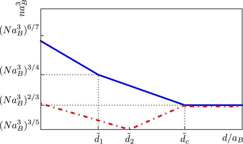
where . At , the critical concentration of MIT, , crosses over to the bulk value Eq. (6). For cm-3 and nm, we get nm. Eqs. (21) and (22) are shown by the blue curve in Fig. 3. At it is higher than the blue curve in Fig. 3. This shows that STO wires are more vulnerable to impurities compared to STO films, because there are less electrons to screen the disorder potential fluctuations.
A.2 Doped STO wire on the insulating STO substrate
In order to emphasize the importance of the dielectric-constant-mismatch effect, we consider a case of doped STO wire on undoped STO grown by MBE, whose and concentration of impurities can be ignored. In this case, the amplitude of potential fluctuations
| (23) |
and is independent on the screening length .
If , then , and gives
| (24) |
where . On the other hand, if , then , and gives
| (25) |
Notice Eq. (25) for a wire is identical to Eq. (18) for a film, and 444This is because we ignore a logarithmic factor in Eq. (16).. At , the critical concentration of MIT crosses over to the bulk value Eq. (6). For cm-3 and nm, nm. Equations. (24) and (25) are shown by the red dot-dashed curve in Fig. 3. At it is substantially higher than the red dot-dashed curve in Fig. 2.
Note that the above estimates of the critical concentration use the typical value of random potential in the STO wire. Strictly speaking, in a wire with large length the chemical potential should exceed the largest potential barrier to make wire conducting. This adds factors proportional to to our above estimates, which were skipped.
In the above discussion we assumed that there are no impurities outside the wire. Now we discuss the case with the same concentration of impurities in the STO substrate, but only wire has concentration of electrons. Then, a cube with side centered around a point of the wire creates a random charge of the order of . At large this charge is larger than total charge of electrons available for the cube screening. This means that the wire can not screen large scale and in the wire of length random potential fluctuations are of the size
| (26) |
Equating and , we obtain the critical concentration as follows
| (27) | ||||
| (28) |
where . Eqs. (27) and (28) are valid if and . Eq. (28) crosses over to the bulk value of Eq. (6) at .
Acknowledgements.
We are grateful to J. Bharat, C. Leighton, D. Maslov, K.V. Reich, and B. Skinner for useful discussions. Y.H. was partially supported by the William I. Fine Theoretical Physics Institute.References
- Spinelli et al. (2010) A. Spinelli, M. A. Torija, C. Liu, C. Jan, and C. Leighton, Phys. Rev. B 81, 155110 (2010).
- Uwe et al. (1985) H. Uwe, R. Yoshizaki, T. Sakudo, A. Izumi, and T. Uzumaki, Japanese Journal of Applied Physics 24, 335 (1985).
- Allen et al. (2013) S. J. Allen, B. Jalan, S. B. Lee, D. G. Ouellette, G. Khalsa, J. Jaroszynski, S. Stemmer, and A. H. MacDonald, Phys. Rev. B 88, 045114 (2013).
- Mott (1969) N. Mott, Phil. Mag. 19, 835 (1969).
- Shklovskii and Efros (1971) B. I. Shklovskii and A. L. Efros, Zh. Eksp. Theor. Fiz. 61, 816 (1971), [Sov. Phys. - JETP 34, 435 (1972)].
- Shklovskii and Efros (2013) B. I. Shklovskii and A. L. Efros, Electronic properties of doped semiconductors, Vol. 45 (Springer, Berlin, 2013).
- Mott (1936) N. Mott, in Mathematical Proceedings of the Cambridge Philosophical Society, Vol. 32 (Cambridge University Press, 1936) pp. 281–290.
- Mansfield (1956) R. Mansfield, Proceedings of the Physical Society. Section B 69, 76 (1956).
- Wemple (1965) S. H. Wemple, Phys. Rev. 137, A1575 (1965).
- Morita (1963) A. Morita, Journal of the Physical Society of Japan 18, 1437 (1963).
- Shimizu (1963) T. Shimizu, Journal of the Physical Society of Japan 18, 1838 (1963).
- Allgaier and Houston (1962) R. S. Allgaier and B. B. Houston, Proc. Int. Conf. Phys. Semiconductors, Exeter , 172 (1962).
- Tufte and Chapman (1967) O. N. Tufte and P. W. Chapman, Phys. Rev. 155, 796 (1967).
- Ambwani et al. (2016) P. Ambwani, P. Xu, G. Haugstad, J. S. Jeong, R. Deng, K. A. Mkhoyan, B. Jalan, and C. Leighton, Journal of Applied Physics 120, 055704 (2016).
- Note (1) In the recent paper Verma et al. (2014) the authors used an unrealistic parameters such as instead of and the effective mass instead of in order to fit data of Ref. Cain et al. (2013). In this way they were able to get inequality , which allowed them to use theory of Ref. Frederikse and Hosler (1967) to predict a saturating behavior for conductivity at large and avoid dealing with compensation. However, as the authors admit there is no justification for using such parameters. In reality, and the theory Mott (1936); Mansfield (1956) is applicable.
- Anderson (1958) P. W. Anderson, Phys. Rev. 109, 1492 (1958).
- Ioffe and Regel (1960) A. F. Ioffe and A. R. Regel, Prog. Semicond. 4, 237 (1960).
- Shklovskii (1973) B. Shklovskii, Fiz. Tekh. Poluprov. 7, 112 (1973), [Sov. Phys. - Semicon. 7, 77 (1973)].
- Keldysh and Proshko (1963) L. V. Keldysh and G. P. Proshko, Fiz Tverd. Tela 5, 3378 (1963), [Sov. Phys. - Solid State 5, 2481 (1964)].
- Gal’pern and Efros (1972) Y. S. Gal’pern and A. L. Efros, Fiz. Tekh. Poluprov. 6, 1081 (1972), [Sov. Phys. - Semicond. 6, 941 (1972)].
- Note (2) We can use analogy with water solutions () of simple salt such as NaCl, where ions and play the role of our donors and acceptors. It is known that at K salt stays dissociated till concentrations as large as cm-3. Here we are dealing with similar , comparable to two hydration radii of ions in water minimum distance between donor and acceptor (lattice constant of STO), but larger and much smaller concentration cm-3. Thus, almost all donor-acceptor pairs should be dissociated at temperature of diffusion freezing in STO.
- Kozuka et al. (2009) Y. Kozuka, M. Kim, C. Bell, B. G. Kim, Y. Hikita, and H. Hwang, Nature 462, 487 (2009).
- Kozuka et al. (2010) Y. Kozuka, M. Kim, H. Ohta, Y. Hikita, C. Bell, and H. Y. Hwang, Applied Physics Letters 97, 222115 (2010).
- Verma et al. (2014) A. Verma, A. P. Kajdos, T. A. Cain, S. Stemmer, and D. Jena, Phys. Rev. Lett. 112, 216601 (2014).
- Liu et al. (2012) Z. Q. Liu, Z. Huang, W. M. Lü, K. Gopinadhan, X. Wang, A. Annadi, T. Venkatesan, and Ariando, AIP Advances 2, 012147 (2012).
- Rytova (1967) N. S. Rytova, Moscow University Physics Bulletin 3, 18 (1967).
- Keldysh (1979) L. V. Keldysh, Soviet Journal of Experimental and Theoretical Physics Letters 29, 658 (1979).
- Cudazzo et al. (2011) P. Cudazzo, I. V. Tokatly, and A. Rubio, Phys. Rev. B 84, 085406 (2011).
- Huang and Shklovskii (2021) Y. Huang and B. I. Shklovskii, “Disorder effects in topological insulator thin films,” (2021), arXiv:2102.00352 [cond-mat.mes-hall] .
- Shklovskii and Efros (1986) B. I. Shklovskii and A. L. Efros, Pis’ma Zh. Eskp. Teor. Fiz. 44, 520 (1986), [Sov. Phys. - JETP Letters 44, 669 (1986)].
- Note (3) In Eq. (16\@@italiccorr) a logarithmic factor is neglected, so the results Eqs. (17\@@italiccorr) and (18\@@italiccorr) are correct up to some logarithmic factors.
- Jena and Konar (2007) D. Jena and A. Konar, Phys. Rev. Lett. 98, 136805 (2007).
- Shklovskii (2017) B. I. Shklovskii, Low Temperature Physics 43, 699 (2017), https://doi.org/10.1063/1.4985976 .
- Petrenko and Bryksa (2014) T. L. Petrenko and V. P. Bryksa, Materials Research Express 1, 025905 (2014).
- Keldysh (1997) L. V. Keldysh, physica status solidi (a) 164, 3 (1997).
- Finkelstein and Ptitsyn (2002) A. Finkelstein and O. Ptitsyn, “Protein physics,” (Academic Press, An Imprint of Elsevier Science, Amsterdam, 2002) Chap. 12.
- Teber (2005) S. Teber, Journal of Statistical Mechanics: Theory and Experiment 2005, P07001 (2005).
- Kamenev et al. (2006) A. Kamenev, J. Zhang, A. Larkin, and B. Shklovskii, Physica A: Statistical Mechanics and its Applications 359, 129 (2006).
- Cui (2006) S. T. Cui, Molecular Physics 104, 2993 (2006).
- Note (4) This is because we ignore a logarithmic factor in Eq. (16\@@italiccorr).
- Cain et al. (2013) T. A. Cain, A. P. Kajdos, and S. Stemmer, Applied Physics Letters 102, 182101 (2013).
- Frederikse and Hosler (1967) H. P. R. Frederikse and W. R. Hosler, Phys. Rev. 161, 822 (1967).