Highly persistent spin textures with giant tunable spin splitting in the two-dimensional germanium monochalcogenides
Abstract
The ability to control the spin textures in semiconductors is a fundamental step toward novel spintronic devices, while seeking desirable materials exhibiting persistent spin texture (PST) remains a key challenge. The PST is the property of materials preserving a unidirectional spin orientation in the momentum space, which has been predicted to support an extraordinarily long spin lifetime of carriers. Herein, by using first-principles density functional theory calculations, we report the emergence of the PST in the two-dimensional (2D) germanium monochalcogenides (GeMC). By considering two stable formation of the 2D GeMC, namely the pure Ge and Janus Ge monolayers ( = S, Se, and Te), we observed the PST around the valence band maximum where the spin orientation is enforced by the lower point group symmetry of the crystal. In the case of the pure Ge monolayers, we found that the PST is characterized by fully out-of-plane spin orientation protected by point group, while the canted PST in the plane is observed in the case of the Janus Ge monolayers due to the lowering symmetry into point group. More importantly, we find large spin-orbit coupling (SOC) parameters in which the PST sustains, which could be effectively tuned by in-plane strain. The large SOC parameter observed in the present systems leads to the small wavelength of the spatially periodic mode of the spin polarization, which is promising for realization of the short spin channel in the spin Hall transistor devices.
-
February 2021
1 Introduction
Finding novel materials with strong spin-orbit coupling (SOC) has been one of the important research themes in the field of spintronics [1]. The large SOC effect is indispensable in spintronics since it could effectively manipulate the spin of electron electrically, which plays a central role in many intriguing phenomena such as spin relaxation [2, 3], hidden spin polarization effect [4, 5, 6, 7], spin Hall effect [8], spin galvanic effect [9], and spin ballistic transport [10]. In a system lacking an inversion center, the SOC induces momentum-dependent spin-orbit field (SOF) lifting Kramer’s spin degeneracy and leading to a complex -dependent spin texture of the electronic bands through the so-called Rashba[11] and Dresselhaus [12] effects. In particular, the Rashba spin texture can be manipulated electrically to produce non-equilibrium spin polarization [13, 14], which has potential application as spin-field effect transistor (SFET) [15, 16]. Although the large SOC is beneficial for spintronic devices, it is also known to induce the undesired effect of causing spin decoherence. In a diffusive transport regime, the momentum-dependent SOF induces spin randomization by a process known as the Dyakonov-Perel spin relaxation [17], which significantly reduces the spin lifetime, and hence limits the performance of the spintronics functionality.
The problem of the spin dephasing by the SOC can be eliminated by designing the materials to exhibit unidirectional SOF. Here, the spin texture is enforced to be uniform and independent of the electron momentum, called the persistent spin texture (PST) [18, 19, 20], arising when the linear Rashba and Dresselhaus contributions compensate each other. Such peculiar spin textures lead to a spatially periodic mode of the spin polarization in the crystal known as persistent spin helix (PSH) mode, enabling long-range spin transport without dissipation [19, 21]. The PST has been previously observed on [001]-oriented semiconductors quantum well (QW) having an equal the Rashba and Dresselhaus SOC parameters [22, 23, 24, 25], or on [110]-oriented semiconductor QW [26] described by the [110] Dreseelhauss model [19]. Similar to the [110]-oriented QW, the PST has also been reported on strained LaAlO3/SrTiO3 interface [27]. Although achieving the PST requires controlling the Rashba and Dresselhaus SOC parameters, it is technically non-trivial since both the parameters are material dependent. This has triggered much attention to finding novel systems where the PST can be observed intrinsically.
Recently, the concept of the PST has been developed in a more general way by enforcing the symmetry of the crystal rather than fine-tuning the SOC parameters. For instant, the PST protected by nonsymmorphic space group has been proposed, as recently reported on various three-dimensional (3D) bulk systems such as BiInO3 with space group [28], CsBiNb2O7 with space group [29], and Ag2Se with space group [30]. Moreover, the symmetry-protected PST with purely cubic spin splitting has been predicted in the 3D bulk materials crystallizing in the and point groups, as found on the 3D bulk Ge3Pb5O11, Pb7Br2F12, and Pb7Cl2F12 compounds [31]. Furthermore, the canted PST has been reported in wurtzite ZnO [100] surface having point group symmetry imposed by the non-polar direction of the surface [32]. In addition, the symmetry-enforced PST has also been observed in several two-dimensional (2D) systems, although it is still very rarely discovered. For the best of our knowledge, only few classes of the 2D materials that has been reported to support the PST including WO2Cl2 monolayer with space group [33] and various group-IV monochalcogenide monolayers with space group such as SnSe [34, 35] and SnTe monolayers [36, 37]. More recently, the PST induced by the lower symmetry of the structure has been predicted on several 2D transition metal dichalcogenides with the line defect [38, 39].
Although the PST has been widely studied in the 3D bulk and QW systems, the search for the ultra-thin 2D materials supporting the PST has lately been very demanding of attention because of their potential for miniaturization spintronic devices [36, 35, 37]. In this work, we predict the emergence of the PST in the 2D germanium monochalcogenides (GeMC) monolayers by using first-principles density functional theory calculations. We have considered two stable formations of the 2D GeMC monolayers, namely the pure Ge and Janus Ge monolayers ( = S, Se, and Te), and found that the PST is observed around the valence band maximum where the spin orientation is enforced by the lower point group symmetry of the crystal. In the case of the pure Ge monolayers, we found that the PST is characterized by the fully out-of-plane spin orientation, which is protected by the point group. On the other hand, the PST is canted in the plane for the case of the Janus Ge monolayers, which is due to the lowering symmetry into point group. More interestingly, we identified large SOC parameters in the spin-split bands where the PST maintains, which could be effectively regulated by applying in-plane strain. The observed large SOC parameter in the present systems results in that the small wavelength of the spatially periodic mode of the spin polarization is achieved. Thus, we proposed the present system as a short spin channel in the spin Hall transistor devices.
2 Model and Computational Details
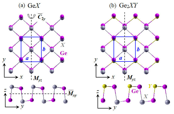
The 2D GeMC monolayers crystallize in a black phosphorene-type structures [40], forming two different stable structures, called as the pure Ge and Janus Ge monolayers [Fig. 1(a)-(b)]. The pure Ge monolayers have or space group characterized by four symmetry operations in the crystal lattice [Fig. 1(a)]: (i) identity operation ; (ii) twofold screw rotation (twofold rotation around the axis, , followed by translation of ), where and is the lattice parameters along and directions, respectively; (iii) glide reflection (reflection with respect to the plane followed by translation ); and (iv) reflection with respect to the plane. By replacing one of the atoms in the Ge monolayers with the atoms, we get the Janus Ge monolayers [Fig. 1(b)]. Here, only the mirror symmetry survives, thus lowering the symmetry into point group.
We have performed non-collinear first-principles DFT calculations using the OpenMX code [41, 42, 43, 44], based on the norm-conserving pseudopotentials and optimized pseudoatomic localized basis functions [45]. The energy cutoff of 350 Ry was used for charge density. The exchange-correlation functional was treated within generalized gradient approximation by Perdew, Burke, and Ernzerhof (GGA-PBE)[46, 47]. We used the -point mesh to discretize the first Brillouin zone. The Pseudo-atomic basis functions of along with the norm-conserving pseudopotentials were used from the OpenMX library. We used the -dependent pseudo potentials where the SOC interaction was included self consistently in all calculations [48].
We calculated the spin textures by deducing the spin vector components (, , ) in the reciprocal lattice vector from the spin density matrix [49]. The spin density matrix, , were calculated using the following relation,
| (1) |
where is the spinor Bloch wave function obtained from the non-collinear first-principles calculations.
-
GeC Monolayers (Å) (Å) (eV) (eV) GeS 3.68 4.40 0.09 1.45 GeSe 3.99 4.39 0.05 1.10∗ GeTe 4.27 4.47 0.02 0.92 Ge2SSe 3.84 4.47 0.08 0.03 1.32 Ge2STe 4.03 4.53 0.06 0.15 0.97 Ge2SeTe 4.14 4.47 0.04 0.05 0.88
To avoid artificial interactions between periodic images created by the periodic boundary condition, we used periodic slab model for both the Ge and Janus Ge monolayers with a sufficiently large vacuum layer (20 Å) in the non-periodic direction. The lattice and positions of the atoms were optimized until the Hellmann-Feynman force components acting on each atom was less than eVÅ where the energy convergence criterion was set to eV. In the case of the Janus Ge monolayers, the energetic stability of the structure is confirmed by calculating the formation energy, , through the following relation,
| (2) |
where , , and are the total energy of Ge, Ge, and Ge, respectively. The optimized structural-related parameters of the Ge and Janus Ge monolayers, and the formation energy of the Janus Ge monolayers are summarized in Table 1, and are in a good agreement overall with previously reported data [36, 50, 51].
3 Results and discussion
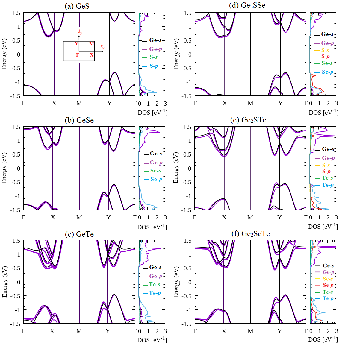
Fig. 2 shows the band structure of various 2D GeMC monolayers calculated along the first Brillouin zone (FBZ) [see the insert of Fig. 2(a)] corresponding to their density of states (DOS) projected to the atomic orbitals. Without the SOC, the GeCM monolayers are semiconductors with an indirect band gap, except for the GeSe monolayer having a direct band gap. The calculated band gap is smaller for the heavier materials (GeTe, Ge2SeTe) and larger for the lighter materials (GeS, Ge2SSe) [see Table 1], which is consistent with previous reports [36, 52, 51]. The valence band maximum (VBM) is located at the line, while the conduction band minimum (CBM) show a different location for the different chalcogen atoms. In the case of the pure Ge monolayers, the CBM is located at the line for both the GeS and GeTe monolayers [Figs. 2(a) and 2(c)], while it is located at the line for the GeSe monolayer [Fig. 2(b)]. In contrast, for the case of the Janus Ge monolayers, the CBM is located at the line, point, and line for the Ge2SSe, Ge2STe, and Ge2SeTe monolayers, respectively [Figs. 2(d)-(f)]. Our calculated DOS projected to the atomic orbitals confirmed that the CBM is mainly originated from the contribution of the Ge- and ()- orbitals, while the VBM is dominated by the Ge- and ()- orbitals.
Turning the SOC leads to a sizable splitting of the bands due to the broken of the inversion symmetry, which is especially pronounced in the bands around the point at the VBM [Fig 2(a)-(f)]. Here, the larger band splitting is identified for the monolayers with heavier elements such as Se and Te atoms. However, we observe the band degeneracy for the along the line in the case of the pure Ge monolayers, which is protected by the and symmetry operations [see Appendix A for detail symmetry analysis]. Conversely, this degeneracy is lifted for the case of the Ge monolayers, which is due to the broken of the and symmetry operations. Since both the the GeTe and Ge2SeTe monolayers have the largest band splitting among the members of 2D GeMC monolayers, in the following discussion, we focused on these monolayers as a representative example of the pure Ge and Ge monolayers, respectively.
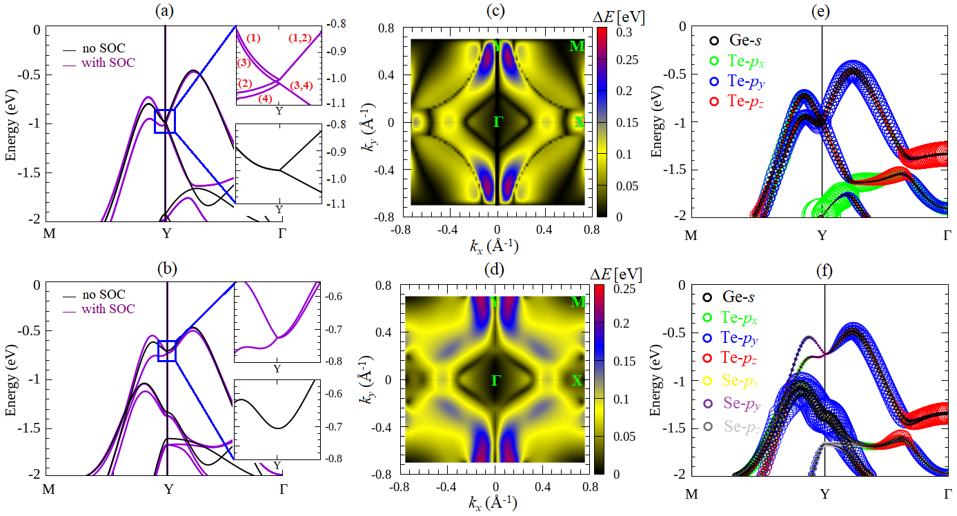
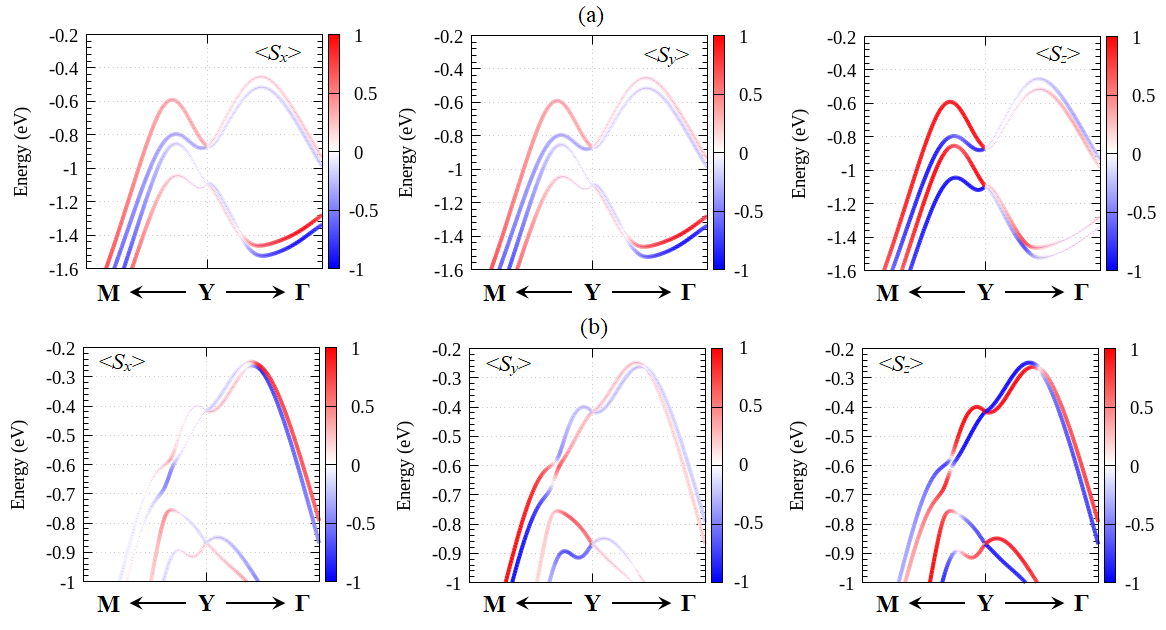
Figs. 3(a)-(b) show the valence band of the GeTe and Ge2SeTe monolayers, respectively, calculated around the point, where the spin-split bands at the VBM are highlighted. Without the SOC, the VBM of the GeTe monolayer exhibits a fourfold degenerate state along the line but splits into two pair doublets along the line [Fig. 3(a)]. When the SOC is introduced, the doublets along the line retain protected by the and symmetry operations [see Appendix A for detail symmetry analysis]. However, along the line, the SOC splits the degenerate states into singlet [Fig. 3(a)], resulting in a strongly anisotropic spin splitting around the point similar to that observed on various 2D group IV monochalcogenide [36, 40, 35]. In contrast, the VBM along the and lines shows a twofold degenerate state for the case of the Ge2SeTe monolayer, which splits into singlet when the SOC is taken into account except for the point due to time reversibility [Fig. 3(b)].
To quantify the spin-split bands, we show in Figs. 3(c)-(d) the calculated spin-splitting energy of the VBM mapped along the entire FBZ for GeTe and Ge2SeTe monolayers, respectively. As expected, along the line, zero splitting energy is observed for the case of the GeTe monolayer [Fig. 3(c)], while the substantially small splitting energy (up to eV) is found in the case of the Ge2SeTe monolayer [Fig. 3(d)]. On the other hand, the large splitting energy up to 0.28 eV (0.23 eV) is achieved along the line at the GeTe (Ge2SeTe) monolayer. By calculating orbitals-resolved projected to bands at near the VBM around the point, we clarified that the large splitting along the line is mainly contributed from the strong hybridization between the orbital of the Ge atom and the orbital of the chalcogen atoms (Te- orbital in the case of the GeTe monolayer and mixing between Se- and Te- orbitals for the case of the Ge2SeTe monolayer) [Fig. 3(e)-(f)]. Remarkably, the calculated splitting energies in both the GeTe and Ge2SeTe monolayers are comparable with that observed on several 2D materials including the pure and Janus transition metal dichalcogenide [0.15 eV - 0.55 eV] [53, 54, 55, 56].
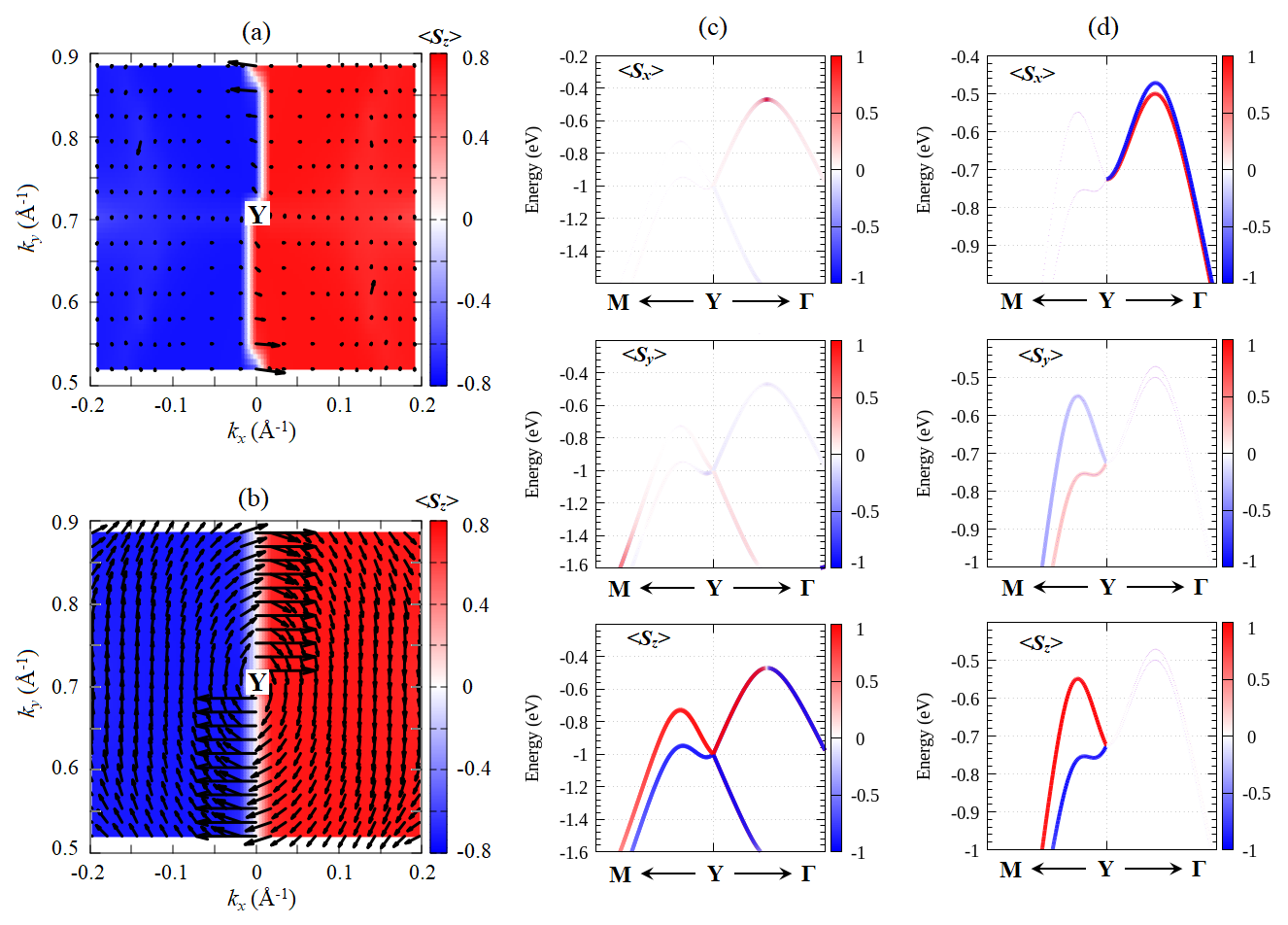
To further demonstrate the nature of the spin splitting, we show in Figs. 4(a) and 4(b) the calculated results of the spin textures around the point near the VBM for the GeTe and Ge2SeTe monolayers, respectively. We also highlight the spin textures by providing the spin-resolved projected to the bands around the VBM along the lines as depicted in Figs. 4(c) and 4(d). It is clearly seen that the spin textures of the GeTe monolayer are characterized by fully out-of-plane spin components , while the in-plane spin components (, ) are almost zero [Figs. 4(a) and 4(c)]. These spin textures are switched from to spin components when crossing at the along () line [Figs. 4(a)]. We noted here that the switching of the spin polarization is also identified at Å-1 along the line [Fig. 4(c)], which is due to the equal population between the and spin-polarized states in the degenerate bands [see Appendix B for the calculated ensemble-average value of the spin components along the line]. These features of the spin textures are notably different either from the Rashba [11] and Dresselhaus [12] spin textures. Moreover, these typical spin textures gives rise to the so-called persistent spin textures (PST) [18, 19, 20], which is consistent with that described by the [110] Dresselhaus model in a [110]-oriented semiconductor QW [19, 26] and similar to that recently reported on various 2D materials such as WO2Cl2 [33], SnSe [34, 35] and SnTe monolayers [36, 37]. The emergence of the PST preserves in the case of the Ge2SeTe monolayer but it shows the different features, i.e., the spin textures are mainly characterized by and spin components, except at (along the line) where the spin component retains [Figs. 4(b) and 4(d)]. Accordingly, quasi-one-dimensional spin textures are observed, which is uniformly tilted from the out-of-plane - to the in-plane -direction at , forming a canted PST in the plane similar to that observed on ZnO (100) surface [32]. The existence of the PST in both the GeTe and Ge2SeTe monolayers is expected to induce a unidirectional SOF, protecting the spins from decoherence through suppressing the Dyakonov-Perel spin-relaxation mechanism [17]. This is highly beneficial to support ultimately long spin-lifetime of carriers [21], which is promising for the realization of an efficient spintronics device.
The physical origin of the band splitting and spin textures observed around the point can be clarified by using a simple Hamiltonian model in the presence of SOC derived from the symmetry of the wave vector . Since the GeTe monolayer possesses point group symmetry at point, the symmetry adapted Hamiltonian can be written in the linear term of the as
| (3) |
where is the nearly-free-hole energy, and are the wave vectors in the - and -directions, respectively, and are the hole effective mass in the - and -directions, respectively, is the -component of the Pauli matrices, and is the SOC parameter in the spin-split bands along the direction [details derivation of the Hamiltonian , see Appendix C].
-
PST Systems (eVÅ) (nm) Reference GeMC GeTe 3.93 6.53 This work Ge2SeTe 3.10 8.52 This work Semiconductor QW GaAs/AlGaAs (3.5 - 4.9) (5.0 - 10) Ref.[22, 23] InAlAs/InGaAs 1.0 - 2.0 Ref.[24, 25] Strained LaAlO3/SrTiO3 7.49 9.8 Ref.[27] Semiconductor Surface ZnO(10-10) surface 34.78 1.9 Ref.[32] 3D Bulk systems BiInO3 1.91 2.0 Ref.[28] CsBiNb2O7 0.012 - 0.014 Ref.[29] 2D systems SnTe 1.2 - 2.85 1.82 - 8.8 Ref.[36, 37] SnSe 0.76 - 1.15 Ref.[35] Doped SnSe 1.6 - 1.76 1.2 - 1.41 Ref.[34] WO2Cl2 0.9 Ref.[33] PtSe2 with line defect 0.2 - 1.14 6.33 - 28.19 Ref.[39] WS2 with line defect 0.14 - 0.26 8.56 - 10.18 Ref.[38]
We can see clearly that the derived in Eq. (3) is only coupled with term, justifying that the spin textures around the point being oriented in the fully out-of-plane -direction. As expected, the out-of-plane PST is achieved, which is consistent-well with the calculated spin textures shown in Figs. 4(a) and 4(c). Moreover, by solving the eigenvalue problem involving the , we obtain that the energy dispersion can be expressed as . This fact implies that the bands are lifted along the line () but are degenerated along the line (), which is in agreement with the calculated band dispersion of the VBM around the point shown in Fig. 3(a). By fitting to the DFT band dispersion of the GeTe monolayer around the point at the VBM, we find that the calculated value of is 3.93 eVÅ, which supports the large spin-splitting energy along the line () in agreement with the DFT results provided in Fig. 3(c).
A similar analysis can also be applied to explain the band splitting and spin textures in the Ge2SeTe monolayer. Here, the lowering symmetry into point group leads to the fact that the Hamiltonian around the point can be expressed as
| (4) |
where , , are the -, -, and -components of the Pauli matrices, respectively, and are the SOC parameters in the spin-split bands along the direction, and is the SOC parameter in the spin-split bands along the direction [details derivation of the Hamiltonian , see the Appendix C].
The first and second terms of in Eq. (4) imposed the spin textures to exhibit the and spin components at , while the spin component retains at due to the third term of the . As a result, the canted PST in the plane is expected at , which matches well with the calculated spin textures obtained from the DFT calculation shown in Figs. 4(b) and 4(d). Moreover, the leads to the energy dispersion, , where is the total SOC parameter defined in the spin-split bands along the direction. Our fitting calculation to the DFT band dispersion of the Ge2SeTe monolayer around the point at the VBM found that the calculated value of parameter (3.10 eVÅ) is much larger than that of the parameter (0.008 eVÅ). The large different value between and indicates that the band splitting is strongly anisotropic between () and () lines, which is consistent with the band dispersion shown in Fig. 3(b). In addition, the large value of parameter implies that the large spin-splitting energy is achieved along () line, which is also consistent with the spin-splitting energy obtained from the DFT calculations described in Fig. 3(d).
We emphasized here that among the member of the 2D GeMC monolayers, the GeTe and Ge2SeTe monolayers have the largest SOC parameter (). Importantly, compared to the other PST systems, the calculated value of in both the monolayers is also the largest of all known PST materials so far [see Table 2]. Moreover, the emergence of the PST in these monolayers leads to the spatially periodic mode of the spin polarization, forming the persistent spin helix (PSH) mode with the wavelength of [19]. We can estimate by considering and parameters obtained from the bands along the line, and find that the calculated value of is about 6.53 nm and 8.52 nm for the GeTe and Ge2SeTe monolayers, respectively. These values of are three-orders of magnitude smaller than that reported on semiconductor QW systems and comparable with that predicted on the 3D bulk PST system such as BiInO3 (2.0 nm) [28] and 2D PST systems including the doped SnSe monolayer (1.2 nm - 1.41 nm) [34] and the SnTe monolayers (1.82 nm - 8.8 nm) [36, 37] [see Tabel 2]. Remarkably, the large SOC parameter () and the small wavelength of the PSH mode () found in the present systems are important for miniaturization of spintronic devices operating at room temperatures.
Next, we discuss the tunability of the observed PST in the GeTe and Ge2SeTe monolayers by introducing an in-plane strain. Here, we consider the strain created by changing the lattice parameters along and directions [see Fig. 1(a)]. We define degree of the strain as , where and are the lattice parameters of equilibrium and strained structures, respectively, calculated along the selected direction. Although the electronic properties of the monolayers are sensitive to the strain, the PST preserves under large strain (up to %) due to the preserving of the crystal symmetry, thus we take it to show the relationship of the SOC parameter () and the strain, which is plotted in Fig. 5(a). We find that stretching or compressing the monolayers significantly changes the magnitude of , i.e., the value of sensitively increases (decreases) under the tensile (compressive) strains [Fig. 5(a)]. For an instant, in the case of the GeTe monolayer, when the tensile strain of % is applied along the () direction, the value of increases up to 6.65 eVÅ (5.75 eVÅ), which is much larger than the original value of 3.93 eVÅ. A similar trend also holds for the case of the Ge2SeTe monolayer where the increasing value of up to 4.57 eVÅ (4.02 eVÅ) is achieved under the tensile strain of % along the () direction. Benefiting from the strong enhancement of by the tensile strains, we should ensure that the wavelength of the PSH mode becomes significantly smaller than that of the original systems [see Fig. 5(b)], which is important for miniaturization spintronic devices.
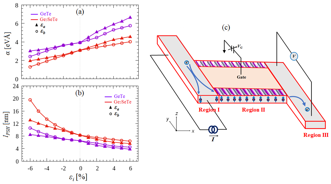
Finally, based on the highly PST found in the present monolayers, we propose a spin Hall transistor (SHT) device as illustrated in Fig. 5(c). Motivated from the previous studies [57, 58], we design the SHT device consisted of three parts, namely, region I, II, and III, representing an injection, gate-controlled, and detector regions, respectively. In region I, the pure spin currents polarized along the out-of-plane () orientation can move to the -direction and are efficiently injected into the middle part of the device (region II) through the direct spin Hall effect (SHE). Subsequently, in region II in which the GeTe (or Ge2SeTe) monolayer is take placed, the out-of-plane spin polarizations effectively induce the PSH mode in the crystal, which could be modulated by the out-of-plane electric field () driven by the gate electrode deposited on the top of the monolayers. Here, as a spin channel of the SHT, the minimum length of the spin channel in region II should be proportional to the wavelength of the PSH mode, . For instant, a very short channel length of about 3.81 nm (5.62 nm) is achieved when the GeTe (Ge2SeTe) monolayer with +6% tensile strain along the direction is used as a spin channel in the region II, which is much smaller than the channel length of the SHT reported on InAs QW system [57]. Moreover, the presence of will determine the on/off logical functionality based on the preserving of the out-of-plane spin polarizations in the PSH mode. When , the out-of-plane spin polarizations are robust to maintain the PSH mode, thus the spin polarizations are efficiently injected into region III without losing the spin information. By utilizing the inverse SHE effect in region III, the out-of-plane spin polarization is converted into the electric currents along the direction, which generates the Hall voltage. In contrast, the PSH mode is broken when is applied [see Appendix D for the spin-resolved bands corresponding to their spin-splitting energy for the systems with an external out-of-plane electric field ], which results in the spin decoherence and significantly decreases the Hall voltage detected in the region III.
We emphasized here that for the realization of the GeTe-based SHT device, the GeTe monolayer should be epitaxially grown on an insulator substrate. Consequently, the crystal symmetry of the GeTe monolayer will be further broken being similar to that of the Ge2SeTe monolayer. In such a situation, the canted PST will maintain the SHT mechanism but with rather lower performance due to the admixtures of the in-plane spin polarization. This effect can be significantly reduced if the GeTe monolayer grown on the insulator substrate has a very small crystal mismatching effect and exhibits a highly ordered structure. Recently, several members of the 2D group IV monochalcogenide family such as SnTe and SnSe monolayers have been successfully synthesized on a properly graphitized SiC substrate [59, 60, 61]. Considering the fact that the GeTe monolayer has the same symmetry as the SnTe and SnSe monolayers, the application of the graphitized SiC substrate for the GeTe-based SHT device is also highly plausible.
4 Conclusion
In summary, we have predicted the emergence of the PST in the 2D GeMC monolayer by performing first-principles DFT calculations combined with the symmetry analysis. We have studied the two stable formations of 2D GeMC monolayers, namely the pure Ge and Janus Ge germanium mochalcogenides (: S, Se, and Te) monolayers and confirmed that the PST is observed around the VBM where the spin orientation is imposed by the lower point group symmetry of the crystal. In the case of the pure Ge monolayers, we have found that the PST is characterized by the fully out-of-plane spin polarization, which is protected by point group symmetry, while the PST is canted in the plane for the case of the Janus Ge monolayers due to the lowering symmetry into point group. More importantly, we have found that the PST sustains in the spin-split bands exhibiting large SOC parameters, which could be effectively controlled by applying the in-plane strains. The larger SOC parameter observed in the present systems leads to the fact that the smaller wavelength of the PSH mode is achieved, which is useful for miniaturization of the spin channel in the spin Hall transistor devices.
Since the PST found in the present study is solely dictated by the and point group symmetries of the crystal, we expect that the similar features are also shared by other materials having similar symmetry. Recently, there are a few other 2D materials that are predicted to maintain the similar symmetry of the crystals, including the 2D ferroelectric Ga ( = S, Se, Te; = Cl, Br, I) family[7] and 2D single-elemental multiferroic materials such as Te, and Bi [62, 63]. Therefore, we have expected that our predictions will stimulate further theoretical and experimental studies in the exploration of the PST systems in the 2D-based materials, thus broadening the range of the 2D materials for future spintronic applications.
Appendix A Symmetry analysis for the band degeneracy along the line in the Ge monolayers
In this appendix, we discuss the origin of the double degeneracy in the band structures of the Ge monolayers along the line in the presence of SOC by considering the symmetry of the wave vector, . The wave vector along the line is invariant under screw rotation and glide mirror reflection. Both the symmetry operations hold the following algebra:
| (5) |
where the minus sign is originated from the fact that two spin rotation operators and are anti-commutative, , so that both and operators are also anti-commutative, , on the line. As a result, for an eigenvector of operator with the eigenvalue of , we obtain the following relation,
| (6) |
The Eq. (6) shows that and are different states with the same eigenvalue, thus ensures the double degeneracy along the line.
Appendix B Spin textures at the VBM along the line
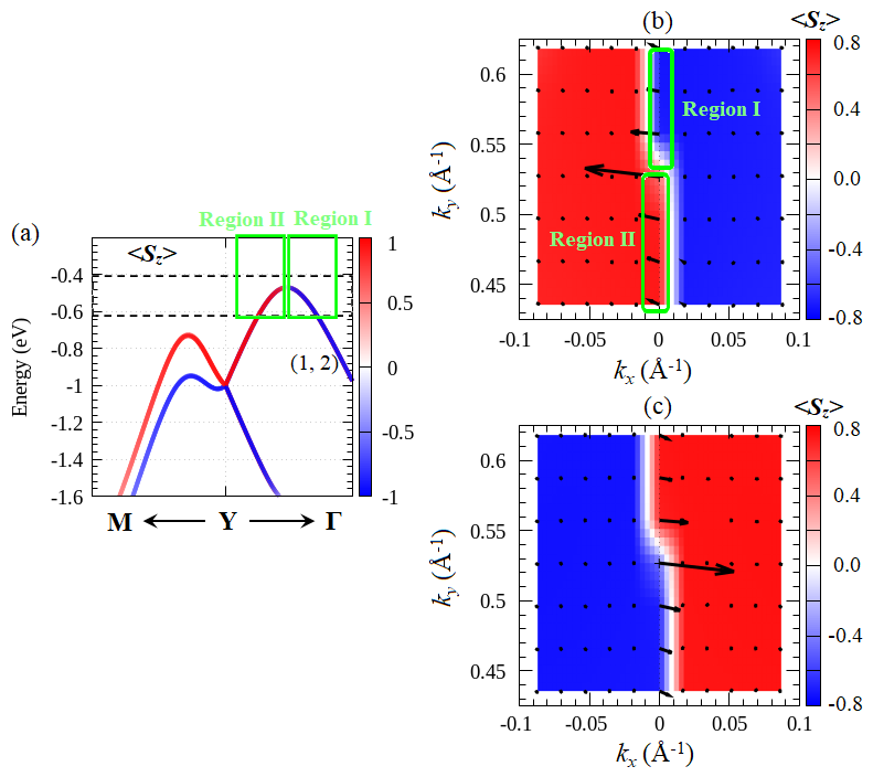
In this section, we present the calculated spin textures of the spin-split bands at the VBM to show the ensemble average values of the spin components along the lines. Here, we calculate the spin textures at an energy ranging from -0.6 eV to -0.4 eV at the VBM [Fig. B1(a)]. The spin textures for the degenerate bands along the lines are shown in Figs. B2(b) and B2(c) for the band (1) and (2), respectively. We find that the switching of the out-of-plane spin components are clearly observed along the when crossing at =0.52. This switching is opposite between state (1) and (2) which has equal populations between and spin components. Such switching of the spin polarization is consistent with the spin-resolved bands shown in Fig. 4(c). Moreover, we also identified the in-plane spin components around =0.52 as indicated by the black arrows in Figs. B1(b) and B1(c), which is also in agreement with the calculated spin projection of the bands presented in Fig. 4(c).
Appendix C Derivation of Hamiltonian
To clarify the observed spin-splitting and the spin textures around the point, we derive an effective Hamiltonian, which can be deduced from the symmetry considerations. Here, we assume that only the linear term with respect to wave vector contributing to the SOC Hamiltonian. We construct the Hamiltonian by identifying all symmetry-allowed term such that the following relation is obtained[64]:
| (7) |
where denotes all symmetry operations belonging to the little group of the wave vector around the point supplemented by time reversal symmetry.
-
Symmetry operations (, ) (, , ) (, ) (, , ) (, ) (, , ) (, ) (, , )
For the case of the GeTe monolayer, the little group of -point is , comprising two mirror symmetry operations, and , and one two-fold rotation around the -axis. Taking into account the transformation role listed in Table B1, the symmetry-allowed linear spin-momentum coupling can be expressed as
| (8) |
In contrast, both and symmetry operations are broken for the case of the Ge2SeTe monolayer. Therefore, the crystal structure of the Ge2SeTe monolayer belongs to the point group. Accordingly, the little point group at the -point also belongs to point group, which comprises only mirror symmetry operation. The effective low-energy Hamiltonian around the point in the Ge2SeTe monolayer can again be deduced by considering only the mirror symmetry operation. By using transformation role given in Table B1 for operation, we obtain the following Hamiltonian,
| (9) |
Appendix D Spin-resolved of the bands under an external out-of-plane electric field
Figs. D1(a)-(b) show the calculated results of the spin-resolved projected to the bands at the VBM around the point for the GeTe and Ge2SeTe monolayers, respectively, under the influence of an external out-of-plane electric field () of 0.1 V/Å. In the case of the GeTe monolayer, we find that the PST is broken by the electric field as indicated by the appearance of the in-plane and spin components in the spin-split bands [Fig. D1(a)]. Similarly, the canted PST in the case of the Ge2SeTe monolayer is also broken by the since the in-plane and spin components appear in the spin-split bands [Fig. D1(b)].
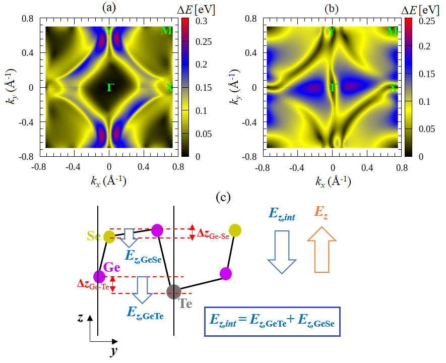
The effect of the on the spin-splitting energy around the VBM is also shown in Figs. D2(a)-(b). In the case of the GeTe monolayer, it is clearly seen that application of the lifts the band degeneracy along the line, where the spin-splitting energy up to 0.1 eV is achieved [Fig. D2(a)]. The emergence of the spin-splitting energy in the GeTe monolayer along the line is due to the fact that both and symmetry operations are broken by the . In contrast to the GeTe monolayer case, the spin-splitting bands of the Ge2SeTe monolayer along the line have already appeared without the [see Figs. 3(b) and 3(d)]. Introducing the in the Ge2SeTe monolayer strongly decreases the spin-splitting energy along the and lines as shown in Fig. D2(b). This is due to the fact that the competition between the internal electric field (induced by the out-of-plane atomic distortion) and the applied electric field decreases the net out-of-plane electric field as schematically shown in Fig. D2(c).
References
References
- [1] Manchon A, Koo H C, Nitta J, Frolov S M and Duine R A 2015 Nat. Matter 14 871 URL http://dx.doi.org/10.1038/nmat4360
- [2] Fabian J and Sarma S D 1999 Journal of Vacuum Science & Technology B: Microelectronics and Nanometer Structures Processing, Measurement, and Phenomena 17 1708–1715 URL https://avs.scitation.org/doi/abs/10.1116/1.590813
- [3] Averkiev N S and Golub L E 1999 Phys. Rev. B 60(23) 15582–15584 URL https://link.aps.org/doi/10.1103/PhysRevB.60.15582
- [4] Zhang X, Liu Q, Luo J W, Freeman A J and Zunger A 2014 Nature Physics 10 387–393 URL https://doi.org/10.1038/nphys2933
- [5] Yuan L, Liu Q, Zhang X, Luo J W, Li S S and Zunger A 2019 Nature Communications 10 906 ISSN 2041-1723 URL https://doi.org/10.1038/s41467-019-08836-4
- [6] Liu K, Luo W, Ji J, Barone P, Picozzi S and Xiang H 2019 Nature Communications 10 5144 ISSN 2041-1723 URL https://doi.org/10.1038/s41467-019-13197-z
- [7] Absor M A U and Ishii F 2021 Phys. Rev. B 103(4) 045119 URL https://link.aps.org/doi/10.1103/PhysRevB.103.045119
- [8] Qi X L, Wu Y S and Zhang S C 2006 Phys. Rev. B 74(8) 085308 URL http://link.aps.org/doi/10.1103/PhysRevB.74.085308
- [9] Ganichev S D, Ivchenko E L, Bel’kov V V, Tarasenko S A, Sollinger M, Weiss D, Wegscheider W and Prettl W 2002 Nature 417 153 URL http://dx.doi.org/10.1038/417153a
- [10] Lu J P, Yau J B, Shukla S P, Shayegan M, Wissinger L, Rössler U and Winkler R 1998 Phys. Rev. Lett. 81(6) 1282–1285 URL http://link.aps.org/doi/10.1103/PhysRevLett.81.1282
- [11] Rashba E I 1960 Sov. Phys. Solid State 2 1224–1238
- [12] Dresselhaus G 1955 Phys. Rev. 100(2) 580 URL https://link.aps.org/doi/10.1103/PhysRev.100.580
- [13] Nitta J, Akazaki T, Takayanagi H and Enoki T 1997 Phys. Rev. Lett. 78(7) 1335–1338 URL https://link.aps.org/doi/10.1103/PhysRevLett.78.1335
- [14] Kuhlen S, Schmalbuch K, Hagedorn M, Schlammes P, Patt M, Lepsa M, Güntherodt G and Beschoten B 2012 Phys. Rev. Lett. 109(14) 146603 URL http://link.aps.org/doi/10.1103/PhysRevLett.109.146603
- [15] Datta S and Das B 1990 Appl. Phys. Lett. 56(7) 665–667 URL http://scitation.aip.org/content/aip/journal/apl/56/7/10.1063/1.102730
- [16] Chuang P, Ho S H, Smith L W, Sfigakis F, Pepper M, Chen C H, Fan J C, Griffiths J P, Farrer I, Beere H E, Jones G A C, Ritchie D A and Chen T M 2009 Nature Nanotechnology 10 35 URL http://dx.doi.org/10.1038/nnano.2014.296
- [17] Dyakonov M I and Perel V I 1972 Sov. Phys. Solid State 13 3023–3026
- [18] Schliemann J, Egues J C and Loss D 2003 Phys. Rev. Lett. 90(14) 146801 URL https://link.aps.org/doi/10.1103/PhysRevLett.90.146801
- [19] Bernevig B A, Orenstein J and Zhang S C 2006 Phys. Rev. Lett. 97(23) 236601 URL https://link.aps.org/doi/10.1103/PhysRevLett.97.236601
- [20] Schliemann J 2017 Rev. Mod. Phys. 89(1) 011001 URL https://link.aps.org/doi/10.1103/RevModPhys.89.011001
- [21] Altmann P, Walser M P, Reichl C, Wegscheider W and Salis G 2014 Phys. Rev. B 90(20) 201306 URL https://link.aps.org/doi/10.1103/PhysRevB.90.201306
- [22] Koralek J D, Weber C P, Orenstein J, Bernevig B A, Zhang S C, Mack S and Awschalom D D 2009 Nature 458 610–613 ISSN 1476-4687 URL https://doi.org/10.1038/nature07871
- [23] Walser M P, Reichl C, Wegscheider W and Salis G 2012 Nature Physics 8 757–762 ISSN 1745-2481 URL https://doi.org/10.1038/nphys2383
- [24] Kohda M, Lechner V, Kunihashi Y, Dollinger T, Olbrich P, Schönhuber C, Caspers I, Bel’kov V V, Golub L E, Weiss D, Richter K, Nitta J and Ganichev S D 2012 Phys. Rev. B 86(8) 081306 URL https://link.aps.org/doi/10.1103/PhysRevB.86.081306
- [25] Sasaki A, Nonaka S, Kunihashi Y, Kohda M, Bauernfeind T, Dollinger T, Richter K and Nitta J 2014 Nature Nanotechnology 9 703–709 ISSN 1748-3395 URL https://doi.org/10.1038/nnano.2014.128
- [26] Chen Y S, Fält S, Wegscheider W and Salis G 2014 Phys. Rev. B 90(12) 121304 URL https://link.aps.org/doi/10.1103/PhysRevB.90.121304
- [27] Yamaguchi N and Ishii F 2017 Applied Physics Express 10 123003 URL https://doi.org/10.7567/apex.10.123003
- [28] Tao L L and Tsymbal E Y 2018 Nature Communications 9 2763 ISSN 2041-1723 URL https://doi.org/10.1038/s41467-018-05137-0
- [29] Autieri C, Barone P, Sławińska J and Picozzi S 2019 Phys. Rev. Materials 3(8) 084416 URL https://link.aps.org/doi/10.1103/PhysRevMaterials.3.084416
- [30] Shi W and Li G 2020 Phys. Rev. B 101(12) 125207 URL https://link.aps.org/doi/10.1103/PhysRevB.101.125207
- [31] Zhao H J, Nakamura H, Arras R, Paillard C, Chen P, Gosteau J, Li X, Yang Y and Bellaiche L 2020 Phys. Rev. Lett. 125(21) 216405 URL https://link.aps.org/doi/10.1103/PhysRevLett.125.216405
- [32] Absor M A U, Ishii F, Kotaka H and Saito M 2015 Applied Physics Express 8 073006 URL https://doi.org/10.7567/apex.8.073006
- [33] Ai H, Ma X, Shao X, Li W and Zhao M 2019 Phys. Rev. Materials 3(5) 054407 URL https://link.aps.org/doi/10.1103/PhysRevMaterials.3.054407
- [34] Absor M A U and Ishii F 2019 Phys. Rev. B 99(7) 075136 URL https://link.aps.org/doi/10.1103/PhysRevB.99.075136
- [35] Anshory M and Absor M A U 2020 Physica E: Low-dimensional Systems and Nanostructures 124 114372 ISSN 1386-9477 URL http://www.sciencedirect.com/science/article/pii/S1386947720309358
- [36] Absor M A U and Ishii F 2019 Phys. Rev. B 100(11) 115104 URL https://link.aps.org/doi/10.1103/PhysRevB.100.115104
- [37] Lee H, Im J and Jin H 2020 Applied Physics Letters 116 022411 URL https://doi.org/10.1063/1.5137753
- [38] Li X, Zhang S, Huang H, Hu L, Liu F and Wang Q 2019 Nano Letters 19 6005–6012 ISSN 1530-6984 URL https://doi.org/10.1021/acs.nanolett.9b01812
- [39] Absor M A U, Santoso I, Yamaguchi N and Ishii F 2020 Phys. Rev. B 101(15) 155410 URL https://link.aps.org/doi/10.1103/PhysRevB.101.155410
- [40] Appelbaum I and Li P 2016 Phys. Rev. B 94(15) 155124 URL https://link.aps.org/doi/10.1103/PhysRevB.94.155124
- [41] Ozaki T, Kino H, Yu J, Han M J, Kobayashi N, Ohfuti M, Ishii F, Ohwaki T, Weng H and Terakura K 2009 http://www.openmx-square.org/
- [42] Ozaki T 2003 Phys. Rev. B 67(15) 155108 URL https://link.aps.org/doi/10.1103/PhysRevB.67.155108
- [43] Ozaki T and Kino H 2004 Phys. Rev. B 69(19) 195113 URL http://link.aps.org/doi/10.1103/PhysRevB.69.195113
- [44] Ozaki T and Kino H 2005 Phys. Rev. B 72(4) 045121 URL https://link.aps.org/doi/10.1103/PhysRevB.72.045121
- [45] Troullier N and Martins J L 1991 Phys. Rev. B 43(3) 1993–2006 URL http://link.aps.org/doi/10.1103/PhysRevB.43.1993
- [46] Perdew J P, Burke K and Ernzerhof M 1996 Phys. Rev. Lett. 77(18) 3865–3868 URL http://link.aps.org/doi/10.1103/PhysRevLett.77.3865
- [47] Kohn W and Sham L J 1965 Phys. Rev. 140(4A) A1133–A1138 URL https://link.aps.org/doi/10.1103/PhysRev.140.A1133
- [48] Theurich G and Hill N A 2001 Phys. Rev. B 64(7) 073106 URL https://link.aps.org/doi/10.1103/PhysRevB.64.073106
- [49] Kotaka H, Ishii F and Saito M 2013 Japanese Journal of Applied Physics 52 035204 URL https://doi.org/10.75672Fjjap.52.035204
- [50] Xu L, Yang M, Wang S J and Feng Y P 2017 Phys. Rev. B 95(23) 235434 URL https://link.aps.org/doi/10.1103/PhysRevB.95.235434
- [51] Seixas L 2020 Journal of Applied Physics 128 045115 URL https://doi.org/10.1063/5.0012427
- [52] Kamal C, Chakrabarti A and Ezawa M 2016 Phys. Rev. B 93(12) 125428 URL https://link.aps.org/doi/10.1103/PhysRevB.93.125428
- [53] Zhu Z Y, Cheng Y C and Schwingenschlögl U 2011 Phys. Rev. B 84(15) 153402 URL https://link.aps.org/doi/10.1103/PhysRevB.84.153402
- [54] Yao Q F, Cai J, Tong W Y, Gong S J, Wang J Q, Wan X, Duan C G and Chu J H 2017 Phys. Rev. B 95(16) 165401 URL https://link.aps.org/doi/10.1103/PhysRevB.95.165401
- [55] Absor M A U, Kotaka H, Ishii F and Saito M 2016 Phys. Rev. B 94(11) 115131 URL https://link.aps.org/doi/10.1103/PhysRevB.94.115131
- [56] Absor M A U, Santoso I, Harsojo, Abraha K, Kotaka H, Ishii F and Saito M 2017 Journal of Applied Physics 122 153905 URL https://doi.org/10.1063/1.5008475
- [57] Choi W Y, Kim H j, Chang J, Han S H, Abbout A, Saidaoui H B M, Manchon A, Lee K J and Koo H C 2018 Nano Letters 18 7998–8002 ISSN 1530-6984 URL https://doi.org/10.1021/acs.nanolett.8b03998
- [58] Sławińska J, Cerasoli F T, Gopal P, Costa M, Curtarolo S and Nardelli M B 2020 2D Materials 7 025026 URL https://doi.org/10.1088/2053-1583/ab6f7a
- [59] Chang K, Liu J, Lin H, Wang N, Zhao K, Zhang A, Jin F, Zhong Y, Hu X, Duan W, Zhang Q, Fu L, Xue Q K, Chen X and Ji S H 2016 Science 353 274–278 ISSN 0036-8075 (Preprint https://science.sciencemag.org/content/353/6296/274.full.pdf) URL https://science.sciencemag.org/content/353/6296/274
- [60] Chang K, Küster F, Miller B J, Ji J R, Zhang J L, Sessi P, Barraza-Lopez S and Parkin S S P 2020 Nano Letters 20 6590–6597 ISSN 1530-6984 URL https://doi.org/10.1021/acs.nanolett.0c02357
- [61] Chang K and Parkin S S P 2019 APL Materials 7 041102 (Preprint https://doi.org/10.1063/1.5091546) URL https://doi.org/10.1063/1.5091546
- [62] Xiao C, Wang F, Yang S A, Lu Y, Feng Y and Zhang S 2018 Advanced Functional Materials 28 1707383 URL https://onlinelibrary.wiley.com/doi/abs/10.1002/adfm.201707383
- [63] Pan Y and Zhou J 2020 Phys. Rev. Applied 14(1) 014024 URL https://link.aps.org/doi/10.1103/PhysRevApplied.14.014024
- [64] Winkler R, Papadakis S, De Poortere E and Shayegan M 2003 Spin-Orbit Coupling in Two-Dimensional Electron and Hole Systems (Berlin: Springer)