Development of an Array of Kinetic Inductance Magnetometers (KIMs)
Abstract
We describe optimization of a cryogenic magnetometer that uses nonlinear kinetic inductance in superconducting nanowires as the sensitive element instead of a superconducting quantum interference device (SQUID). The circuit design consists of a loop geometry with two nanowires in parallel, serving as the inductive section of a lumped LC resonator similar to a kinetic inductance detector (KID). This device takes advantage of the multiplexing capability of the KID, allowing for a natural frequency multiplexed readout. The Kinetic Inductance Magnetometer (KIM) is biased with a DC magnetic flux through the inductive loop. A perturbing signal will cause a flux change through the loop, and thus a change in the induced current, which alters the kinetic inductance of the nanowires, causing the resonant frequency of the KIM to shift. This technology has applications in astrophysics, material science, and the medical field for readout of Metallic Magnetic Calorimeters (MMCs), axion detection, and magnetoencephalography (MEG).
Introduction
Highly sensitive magnetic sensors are useful in many fields, particularly in astronomy, medicine, and geology. [squidgeophys, squidbiomag, clarke2006squid] Currently, the Superconducting QUantum Interference Device (SQUID) is the most sensitive magnetometer, with a sensitivity of [clarke2006squid]. Arrays of SQUIDs have been used for time division multiplexing (TDM) of superconducting detectors for over a decade [irwin2002]. However, scaling to the increasing number of detectors used in modern instruments is challenging partly because the SQUID requires multiple layers during fabrication, which increases time and cost to make arrays [kpup]. A recent development called MUX attempts to couple each SQUID to a corresponding transmission line resonator to achieve frequency domain multiplexing (FDM) with a high multiplexing factor. This uses an RF SQUID coupled to a modulation coil to counteract the periodic nature of the device, and a load inductor to couple to the resonator for readout. Each resonator has a unique resonant frequency, and is shifted by the change in inductance in the RF SQUID [uMUX] [doi:10.1063/1.1791733] [doi:10.1063/1.4829156].
In addition to improving SQUID readout, there has been some publication on using Dayem bridges instead of Josephson Junctions. [doi:10.1063/1.4948477] Using a Dayem bridge and a small SQUID diameter, one group was able to achieve 50 [SQUIDtinyFLUX] Furthermore, it has been shown that kinetic inductance rather than magnetic inductance can modulate nanoSQUIDs, effectively reducing the size of the device by an order of magnitude. [nanoSQUID]
Alternatively, two groups independently developed a superconducting magnetic sensor that uses nanowires with high kinetic inductance instead of Josephson Junctions as the sensing component [kpup] [KIM_Nature]. These devices are similar to the Lumped Element Kinetic Inductance Detector (LEKID) in that they are planar lumped element devices and use superconductors which have high nonlinear kinetic inductance. However, they have not been able to achieve SQUID sensitivity or develop an array of magnetometers. This paper aims to demonstrate an array of KIMs read out using FDM and a discussion on its sensitivity. The KIM can be used for magnetic field sensing, direct readout of magnetic x-ray detectors, and current-coupled readout. [kpup] [KIM_Nature] [Asfaw_2018]
Operating Principles
The kinetic inductance of a nonlinear superconducting thin film in which the thickness, is much less than the penetration depth, can be expressed by
| (1) |
where is the characteristic current dependent on the material and geometry of the film that sets the nonlinearity of the film, and is the kinetic inductance of the superconductor with no bias current, . The superconductor is at its peak nonlinearity when biased close to .
When formed into a loop, the superconductor obeys the following expression:
| (2) |
in which is the shielding current induced by the bias field, the total inductance, includes the geometric term and the kinetic inductance of the material, is the bias flux, and is an integer multiple of , the flux quantum. When the loop is biased with a magnetic flux perpendicular to its plane, the superconductor generates an opposing shielding current, which from looking at Eq. 1, determines the kinetic inductance. If there is a perturbation in the flux, the kinetic inductance of the loop will change. When the loop is incorporated into a resonator, the change in kinetic inductance can be seen as a shift in resonance, . [kpup] [KIM_Nature] [Asfaw_2018]
Experiment
Design
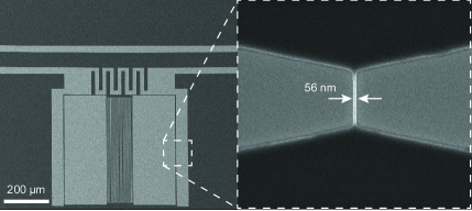
The KIM is a microwave resonator coupled to a CPW transmission line via an interdigitated coupling capacitor. The resonator consists of two nanowires acting as inductors in parallel with an interdigitated resonant capacitor. Both capacitors are interdigitated to reduce two-level system (TLS) noise and the geometry of the nanowires are kept small ( 50nm, 20nm) to maximize , the kinetic inductance fraction of the device. TLS noise originates from coupling between the resonator and electric dipole moments on the substrate/superconductor interface. [Noroozian_2009] [doi:10.1063/1.2711770] There are four chips, each with an array of 8 resonators, where the resonant capacitor varies in each device. NbN was chosen to be the device material due to its high kinetic inductance. The nanowire length for each array was chosen to be 250nm, 500nm, 750nm, and 1m.
Fabrication
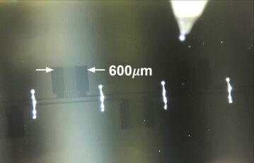
The KIM arrays were fabricated from a -thick niobium nitride (NbN) film. NbN was reactively sputtered at room temperature on a high-resistivity silicon wafer [dane2017bias]. The room-temperature sheet resistance was per square, the critical temperature was , and the critical current was roughly 50A. The arrays were patterned using -electron beam lithography with ZEP530A positive tone resist. The patterns were transferred into NbN with CF reactive ion etching (more fabrication details are reported in previous publications on superconducting nanowire single photon detectors [najafi2014fabrication, yang2005fabrication]). Fig. 2 shows optical and scanning electron micrographs of the fabricated device.
Test Setup
An in-house Helmholtz coil made with superconducting wire and calibrated with a commercial hall sensor was used to bias the