Thermoelectric effects at a Germanium-electrolyte interface:
measuring temperature oscillations at room temperature
Abstract
We describe measurements of temperature oscillations at room temperature, driven at the complex interface between p-doped Germanium, a nm size metal layer, and an electrolyte. We show that heat is deposited at this interface by thermoelectric effects, however the precise microscopic mechanism remains to be established. The temperature measurement is accomplished by observing the modulation of black body radiation from the interface. We argue that this geometry offers a method to study molecular scale dissipation phenomena. The Debye layer on the electrolyte side of the interface controls much of the dynamics. Interpreting the measurements from first principles, we show that in this geometry the Debye layer behaves like a low frequency transmission line.
Keywords Debye layer, Peltier effect, thermoelectric coefficients, THz spectroscopy
I Introduction
Boundary layers are ubiquitous non-equilibrium structures at solid-fluid interfaces.
They are in general loci of interesting dynamical behavior, through their transport properties and instabilities.
The boundary layer is a region of large gradient of a field: in a fluid mechanics context this is typically
the velocity field, but also the temperature field in the case of thermal convection. In solid state, we have
the depletion layer at a semiconductor junction. In a neutral electrolyte, the Debye layer at a solid - fluid interface
is similarly a region of large gradient of the electrostatic potential, i.e. large electric field.
Here we describe two different dynamical effects which arise
in an experimental setup where we force the Debye layer at low frequencies with an external
electric field. In the experiment, the role of the Debye layer is essentially that of a distributed
capacitance: it is the source for the capacitive current which drives the thermoelectric effects
which we observe. By “thermoelectric effects” we mean generally heat sources
at an interface which are proportional to the electrical current, not the current squared.
The Debye layer itself, under the circumstances of the experiment, behaves like an RC transmission line,
which is the second somewhat unfamiliar dynamical effect which we describe.
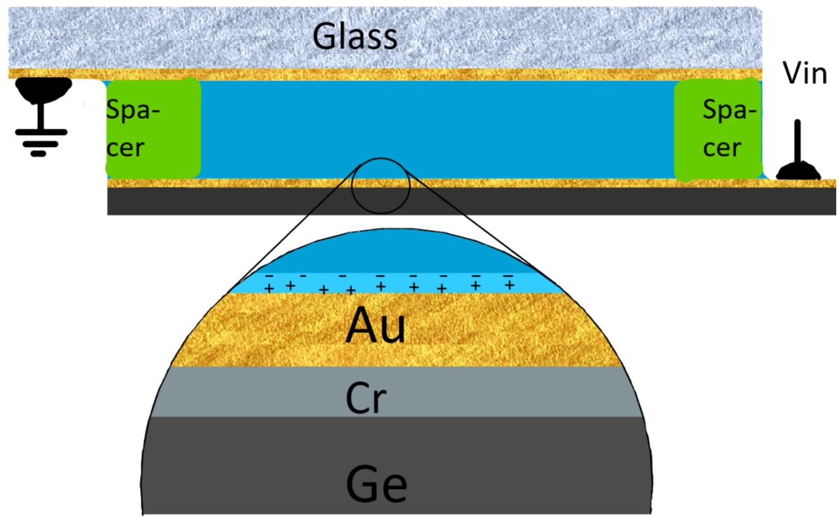
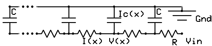
(b) The Ge-metal-Debye-layer strip is electrically similar to an RC transmission line: the longitudinal resistance comes from the Ge and metal layers, the capacitance comes from the Debye layer. The capacitive current is responsible for the thermoelectric effect.
Thermoelectricity has been known for two centuries, yet to this day there are new developments
in the field (for a relatively recent review see [1]), especially in the context of designing materials
and geometries with optimized properties for energy conversion [2, 3, 4]. Thermoelectric devices at the sub- scale represent a new and interesting field of research,
also leading to the desire to develop new techniques for local temperature measurements at the
to scale [5].
Thermoelectric effects at the solid - liquid interface, more specifically, are relevant
in a variety of different settings,
from the technology of crystal growth [6] to devices such as
electrolyte gated transistors [7, 8].
Our experiment was originally concieved to study dissipative phenomena at the solid - liquid
interface, so we set up to measure far infrared (IR) radiation emitted from that region.
Here we show that in our geometry, one can measure driven temperature oscillations of the solid-liquid interface
of order at room temperature. This resolution should allow to investigate by this method dissipative
phenomena such as the internal dissipation of a driven molecular layer [9, 10], and in general hydrodynamic dissipative phenomena down to the molecular scale.
II Experimental results
The setup we wish to consider consists of a thin conductive slab in contact with an aqueous
electrolyte. Specifically, we start from a p-doped Ge wafer of thickness . Ge is
used because (unlike water) it is relatively transparent to THz radiation in the wavelength range
we wish to detect (). Using vacuum evaporation we deposit on one side
of the wafer a thick Cr layer followed by a Au layer. The wafer is then cut into
pieces roughly in size, and a rectangular
chamber is constructed having the Ge chip as its “bottom”, a gold evaporated microscope slide as its
“top”, separated by thick spacers (Fig. 1(a)).
Electrical contacts are added at one end of this construction,
and the chamber is filled with the electrolyte (a buffered solution of saline-sodium citrate (SSC) in water,
see Mat. & Met.). The Ge side of the chamber is placed directly in front of the entrance window of a
liquid nitrogen cooled HgCdTe far infrared detector. The geometry is such that the
size detector “sees” only a small area at the center of the chamber. The experiments consist of exciting
the chamber with a sinusoidal voltage in the frequency range (and amplitude
, below the threshold for water hydrolysis) and recording the intensity of emitted IR radiation
in a phase locked loop. The measurement is sensitive to radiation in the wavelength
range (); for comparison, a room temperature photon has a wavelength
.
Fig. 2 shows the amplitude of the current injected into the device vs the frequency of the applied voltage. Overall the response is that of an RC circuit (solid line), with , ,
.
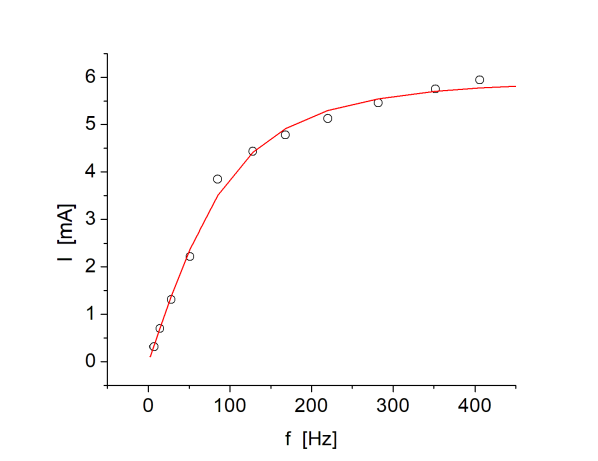
The resistance comes from the longitudinal resistance of the Ge and metal layers, while the capacitance
comes from the Debye layer. The latter can be estimated as: (in esu),
where is the dielectric constant of water, the surface of the chamber,
the Debye length; this gives . The equivalent discrete elements
circuit is an rc transmission line, sketched in Fig. 1(b).
It is the capacitive current in this transmission line
which drives the thermoelectric effect we will now describe. This capacitive current originates from switching
the polarity of the Debye layer as the voltage alternates, and is carried by ions in the electrolyte, and by
electrons and holes in the metal layers and the p-doped Germanium.
Our main result is displayed in Fig. 3, which shows the intensity of IR radiation seen by the detector vs
frequency of the driving voltage. There are several notable features. First, this is the signal at the first harmonic
(same frequency as the drive); there is no measurable signal from the IR detector at the second
harmonic (), or any other higher harmonics. Thus the IR emission does not come from Joule
heating in the device (which would create a signal at the second harmonic), or, to say it differently, the
infrared emission is proportional to the current, not the current squared. Second, what might look like a
resonance is in fact the combination of two different phenomena: the increase in the capacitive current
with frequency, and thermal diffusion away from the quasi-2D, solid - liquid interfacial region which is being
alternately heated and cooled by thermoelectric effects.
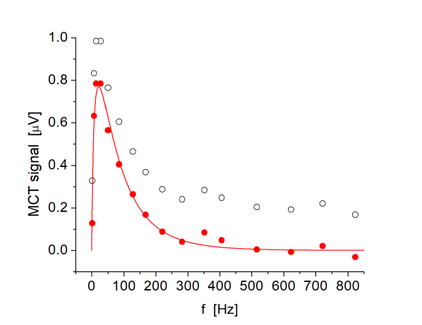
The open circles in Fig. 3 represent the measurements of intensity of IR radiation reaching the detector,
after subtraction of a background which comes from inductive pickup, from the circuit driving the device,
and from the device itself. In practice, we measure this background at various drive frequencies by blocking
the entrance window to the detector; the measured background is proportional to the drive frequency
: the corresponding straight line has been subtracted from the intensity measurements to obtain
the open circles in Fig. 3. The filled circles are the same data as the open circles,
after subtraction of a constant
(independent of ) electronic offset determined by requiring for
, that is, we subtract the value of the high frequency plateau seen in the data
points represented as open circles. That plateau results from imperfect offset trimming of the operational amplifier
in the detection circuit, and is also of the same order (twice as large) as the intrinsic noise of the experiment
due to fluctuations in black body background radiation.
Based on the quantitative analysis of the next section, our interpretation of these measurements is that
the capacitive current due to building up the Debye layer in the elctrolyte alternately heats and cools the
quasi-2D region at the solid - liquid interface, through a thermoelectric effect. The amplitude of the corresponding
temperature oscillations depends on the driving frequency , because of heat diffusion away from
the interface. The temperature oscillations produce a corresponding amplitude modulation of the black body
radiation emitted from the region of the interface, which is the signal we detect.
III Theory
We consider a situation where the 2D solid - liquid interface is heated (or cooled) by a heat current proportional to the capacitive current :
| (1) |
where is a thermoelectric coefficient (the Peltier coefficient if the mechanism is the Peltier effect). Choosing a z axis perpendicular to the interface (at ) and going into the Germanium, the capacitive current on the Ge side () is
| (2) |
in the z direction; is the step function ( for and for ). Writing the conservation of energy then leads to the following diffusion equation for the temperature field (on the Ge side):
| (3) |
where is the heat diffusion constant of the Germanium, and
| (4) |
and are the density and specific heat for Ge, is the Dirac delta function. Writing (with the convention that the physical quantities are the real part of the complex ones) the general solution of (3) is:
| (5) |
where
| (6) |
with the constants and to be determined by the boundary conditions.
Integrating (3) in the neighborhood of gives:
| (7) |
In the experiments, the heat flow problem at (the solid - liquid interface) and ( is the thickness of the Ge) is not well defined, because neither do we control the heat current nor the temperature. We will assume symmetric conditions at : , then using (7) the boundary condition at is
| (8) |
Alternatively, if we assume no heat flux into , then the boundary condition is . At the other end (), we assume efficient removal of extra heat by convection in the air, i.e.
| (9) |
With these boundary conditions, the solution (5) becomes:
| (10) |
Thus the amplitude of the temperature oscillation at the interface is
| (11) |
We are also interested in the temperature oscillation averaged over the Ge thickness; the corresponding amplitude is, using (10) :
| (12) |
We expect the signal detected in the experiments to be proportional to the expression (12) (or perhaps (11)), since the power emitted per unit surface from black body radiation, given a temperature modulation of amplitude around room temperature , is:
| (13) |
is the Stefan - Boltzmann constant and () the emissivity of the emitting surface. The parameter in (12) and (11) is proportional to the amplitude of the capacitive current (see (4)), which is given by the measured RC response of the cell (Fig. 2):
| (14) |
where is the area of the cell.
A fit of the data in Fig. 3 using either (12) or (11) is
a stringent requirement, since all parameters are known, except for an overall multiplicative constant
(which contains the calibration of the IR detection system). However, upon attempting this one-parameter
fit, it is apparent that the frequency dependence expressed by (12) or (11) is not the correct one vis-a-vis the measurements. What is missing from our
theory is consideration of how the driving voltage travels along the Debye layer, which introduces an
additional frequency dependence to the capacitive current at the point of measurement. We now analyze
this interesting phenomenon. Consider the Ge chip coupled to the electrolyte: the Ge (and metal
layers) act as a distributed resistance, while the Debye layer acts essentially as a distributed
capacitance. The result is an RC transmission line (Fig. 1(b)), which we model
in 1D; the governing “cable equation” for the voltage is then:
| (15) |
i.e. the diffusion equation with diffusion constant ; is the resistance per unit length, the capacitance per unit length. The capacitive current per unit length (i.e. the current going into the Debye layer) is
| (16) |
We consider a sinusoidal input at : and, for simplicity, a semi-infinite cell (so that for ); then the solution of (15) is:
| (17) |
| (18) |
so that
| (19) |
where is the observation point with respect to the length of the cell . To relate the physical system (a strip of length and width ) to this 1D model we note that the capacitive current density is while is the capacitance per unit area; is the total capacitance of the cell, the total resistance (these are measured in Fig. 2). If we describe the thermoelectric effect through a Peltier coefficient (see (1)), then and putting all the pieces together (12) reads:
| (20) |
is the observation point; we treat it as a geometric parameter of order 1, which we are
allowed to fit (considering that the real system is 2D, with imperfectly known geometry of the contacts, etc.).
If instead of (12) we use (11) we find the amplitude of the
temperature oscillation at the interface as:
| (21) |
Comparing (20) with the measurements of Fig. 3 is a stringent test, as there are only two fitting parameters: an overall multiplicative factor (which encompasses the detector calibration, among other factors), and the dimensionless number (which is basically a geometric factor). All other parameters are measured or known: (thickness of the Ge slab), (measured, see Fig. 2), (thermal diffusion constant for Ge). Fig. 3 shows that the form (20) fits the measurements very well (solid line in the figure). Using the temperature oscillaton at the interface (21), instead of the averaged quantity (20), results in an essentially identical fit. In summary, the mechanism we identified for the observed frequency dependence of the IR emission - namely, heat transport to and from the 2D solid-liquid interface by thermoelectric effects - appears to be correct.
IV Discussion
The fit of Fig. 3 shows that the dependence of the emitted radiation on the driving frequency
is well captured by the theory (20) or (21),
but it is also instructive to consider the
absolute magnitude of the corresponding temperature oscillation. According to the factory calibration of our
MCT detector (dark resistance at ), the change in resistance per unit
incident intensity is for black body radiation at
. With our electronics (see Mat. & Met.) this figure translates to the following calibration for the
measurements of Fig. 3:
a signal corresponds to an incident intensity .
There is a correction because in the experiment the radiation is at , which we ignore for the moment.
Using the Stefan - Boltzmann law, the intensity (power per unit surface) of black body radiation emitted by
the heated interface at the driving frequency is
| (22) |
where , is the Stefan - Boltzmann constant, and we are using the averaged amplitude of the temperature oscillation, , for now. is the effective emissivity of the cell (), which we discuss later. Thus the amplitude of temperature oscillation which, in the experiment, corresponds to a signal is:
| (23) |
If we assume for now , this expression gives
.
What is the actual effective emissivity to be used in (23) is not completely clear, because
our cell is a composite Germanium - metal - water structure, but we reason as follows. The
thick Ge slab alone would have very small emissivity in the infrared range we are
considering, because the slab is essentially transparent in that range. The inverse absorption length in Ge
at a wavelength is , which gives the fraction
of intensity absorbed by the slab as ; this is also
the emissivity (i.e. ). Ignoring the nm size metal layers, the water in close proximity to the interface
is on the other hand an effective black body emitter. The emissivity of bulk water in the far infrared
() is , while the inverse absorption length is
, thus already a thick layer
of water forms an effective black body emitter at our wavelengths. The thermal diffusion time across this
water layer is ( is
the thermal diffusion constant of water). Since the thermal diffusion constant of Germanium is more than
100 times larger than , the picture we arrive at is that while the temperature dynamics is controlled
by the Ge slab, the black body emissivity is controlled by this thick water layer at the
interface, at least for driving frequencies . Therefore we should use an emissivity
, and taking into account a transmittance of the Ge exit surface (the Ge - air interface) of
, we arrive at an effective emissivity for the cell of . Also, from
the preceding discussion we expect that what matters for the IR emission is the amplitude of the temperature
oscillation at the interface, , rather than the amplitude
averaged over the Ge slab. With we then find from (23) that
the amplitude of temperature oscillation at the interface corresponding to a signal in the experiment
(see Fig. 3) is .
We should also take into account the difference between
the factory calibration of the MCT detector using black body radiation
and the experiment with radiation at (see Mat. & Met.). From the spectral
sensitivity of the detector given by the manufacturer and the black body spectra at
and we find that the calibration above needs to be adjusted by a factor ,
so that the temperature oscillation corresponding to a signal in the experiment is
(assuming an effective emissivity ) :
| (24) |
With this calibration, the measured amplitude of temperature oscillation e.g. at is, from Fig. 3,
| (25) |
Let us now see what is the magnitude of the temperature oscillation predicted by the theory (21). Let us take again the driving frequency . Since , then (thus the wavelength of the damped voltage oscillation in the transmission line is at this frequency), and . Then (recall that ) and expanding the exponentials one finds:
| (26) |
and the expression (21) becomes:
| (27) |
Incidentally, in the same approximation one finds that the expression for the averaged amplitude (20) differs from the present one only by an overall factor of 2: . To evaluate , we use (in esu), from the measured capacitance (Fig. 2) and area of the cell. Further, , , ; (from the fit Fig. 3) , (from the fit Fig. 2), giving . The Seebeck coefficient for p-doped Ge, at our carrier concentration and room temperature, is approximately [11]. Through the Kelvin relation, the corresponding Peltier coefficient is . Using this value, we obtain and finally at . This is a factor 2 smaller than the measured amplitude according to (25). However, given the lack of an independent experimental calibration of our temperature measurements, and also considering that the thermal boundary conditions leading to (27) are not well defined in the experiment, it is not clear that this discrepancy is significant. Nonetheless, we mention two other mechanisms which might contribute to the observed thermoelectric effect. The first is non-radiative electron-hole recombination in the depletion layer at the Ge - metal interface. Ge is an indirect gap semiconductor and non-radiative (phonon dependent) recombination dominates over direct transitions, especially in the presence of surface defects (“traps”). Junctions between p-doped Ge and a metal are typically ohmic, due to Fermi level pinning near the edge of the valence band [12]. In such a junction, recombination in the depletion region can be the dominant conduction mechanism [13, 14]. If electron-hole recombination is the origin of our thermoelectric effect, we simply should replace the Peltier coefficient in (21) with where is the band gap, the elementary charge. Namely, the source term in the diffusion equation (3) is, in the case of electron-hole recombination,
using the notation of Section III; is the capacitive current. In the case of the Peltier effect, the source term is
where is the heat current, so we see that turns into . With this modification in (21) and (27) we now find:
| (28) |
This figure is now larger than the measurement (25) by about a factor of .
But again, considering the uncertainties in estimating the effective emissivity of the cell,
and also the somewhat arbitrary “symmetric” boundary condition (8)
used in the calculation, there is reasonable agreement between theory and experiment on the
absolute magnitude of the measured effect, whether we attribute (most of) this particular thermoelectric effect
to electron-hole recombination or the the Peltier effect in the germanium.
Yet another possibility is an anomalously large Peltier coefficient of the electrolyte, in our geometry.
There have been recent theoretical proposals about large thermoelectric response of electrolytes
at the scale of the Debye layer [15, 16]. These studies suggest that Seebeck coefficients
as large as may be obtained in electrolyte filled nanochannels [16],
which corresponds to
Peltier coefficients of order , up to 8 times larger than for our Germanium.
This effect could thus be relevant to our measurements. While the situation considered in the above studies
was for a flow of ions and corresponding temperature gradient parallel to the Debye layer
(along the nanochannel), similar effects could arise in our geometry too. In general, the microscopic
origin of the thermoelectric effect we measure is an interesting question, which can be answered
experimentally, once we reopen our UCLA lab “after the plague”.
Let us summarize. We have introduced an experimental configuration where the Debye layer
at the solid - electrolyte interface acts as the distributed capacitance of an RC transmission line, the
semiconductor chip acting as the distributed resistive part. One motivation in constructing and analyzing
such a system is that a similar configuration forms the passive part of the transmission line of
the axon in the neuron [17], where the cell membrane is the distributed capacitance, while
the electrolyte in the confined space inside the axon acts as the distributed resistance. We have been
experimenting with creating an artificial axon [18, 19], and are thus interested
in the dynamics of such systems.
An electrical current at the junction between two different conductors will in general give rise to
thermoelectric effects. We were able to measure and quantitatively describe such a thermoelectric effect
in a rather unfamiliar configuration. Consideration of similar effects is however relevant in the field of
mixed electronic - ionic devices, for example, electrolyte gated transistors. In the course
of this study we found that, in our simple setup, we are able to measure driven temperature fluctuations
of the 2D solid-liquid interface of order , at room temperature. There are not too many
methods offering a combination of temperature resolution and space resolution in at least one dimension.
For example, temperature mesurements with a space resolution of order in all three dimensions
are feasible using the optically detected electron spin resonance in nitrogen vacancy centers in diamond
[20]; the temperature resolution is a fraction of .
Even higher spatial resolution in two out of three
dimensions can be obtained with electron microscopy based techniques, such as
Plasmon Energy Expansion Thermometry [21, 22],
while the temperature resolution is still of order .
One can of course do much better in terms of temperature resolution if one abandons spatial resolution;
for instance, a recent experiment based on a resonant optical cavity
achieved a temperature resolution of order at room temperature [23].
While breaking no barriers in either temperature or space resolution separately, the remarkable sensitivity
of our setup in the context of a driven 2D interface should allow for studies of dissipative dynamics
at the nm scale and room temperature. For instance, consider a layer of deformable
macromolecules attached to the gold layer in our setup. As an example, take a globular protein of typical
size . The protein can be deformed by the large electric field at the Debye layer
[24]; deformations beyond the linear elasticity regime can be achieved [25, 26],
which are then dissipative [9, 10]. If is the number of molecules per unit surface
and the energy per molecule dissipated per cycle of the electric field, then the power dissipated
per unit surface at the gold - electrolyte interface is . If we take as reasonable
values ,
(corresponding to breaking 1 - 2 hydrogen bonds while deforming the molecule),
at driving we get . By comparison,
in the measurements of Fig. 3 the power per unit surface deposited at the interface by the
thermoelectric effects described is (if we consider electron-hole recombination as the mechanism)
where is the capacitive current. At
driving, this gives and
, same as the source term above. Thus, in this
hypothetical example we would be able to detect a signal from the internal dissipation of a molecular layer
with a signal over background ratio of order 1. In general, it seems possible to study dissipative phenomena
at the scale of the Debye layer with this method.
Acknowledgements.
This work was supported by NSF grant DMR - 1809381.References
- Shakouri [2011] A. Shakouri, Annu. Rev. Mater. Res. 41, 399 (2011).
- Hicks and Dresselhaus [1993] L. D. Hicks and M. S. Dresselhaus, Phys. Rev. B 47, 12727 (1993).
- Ohta and et al [2007] H. Ohta and et al, Nature Materials 6, 129 (2007).
- May and Sales [2021] A. May and B. Sales, Nature Materials https://doi.org/10.1038/s41563-020-00908-x (2021).
- Hubbard et al. [2020] W. A. Hubbard, M. Mecklenburg, J. J. Lodico, and B. C. Regan, ACS Nano 14, 11510 (2020).
- Wiegel and Matthiesen [1997] M. E. Wiegel and D. H. Matthiesen, Journal of Crystal Growth 174, 194 (1997).
- Palazzo and et al [2015] G. Palazzo and et al, Adv. Mater. 27, 911 (2015).
- Dorfman et al. [2020] K. D. Dorfman, D. Z. Adrahtas, M. S. Thomas, and C. D. Frisbie, Biomicrofluidics 14, 011301 (2020).
- Ariyaratne et al. [2014] A. Ariyaratne, C. Wu, C.-Y. Tseng, and G. Zocchi, Phys. Rev. Lett. 113, 198101 (2014).
- Alavi and Zocchi [2018] Z. Alavi and G. Zocchi, Phys. Rev. E 97, 052402 (2018).
- Ohishi and et al [2016] Y. Ohishi and et al, Jpn. J. Appl. Phys. 55, 051301 (2016).
- Nishimura et al. [2007] T. Nishimura, K. Kita, and A. Toriumi, Appl. Phys. Lett. 91, 123123 (2007).
- Hall [1952] R. N. Hall, Phys. Rev. 87, 387 (1952).
- Rhoderick [1982] E. Rhoderick, IEE Proc. 129, 1 (1982).
- Dietzel and Hardt [2016] M. Dietzel and S. Hardt, Phys. Rev. Lett. 116, 225901 (2016).
- Fu et al. [2019] L. Fu, L. Joly, and S. Merabia, Phys. Rev. Lett. 123, 138001 (2019).
- Koch [1999] C. Koch, Biophysics of Computation (Oxford University Press, 1999).
- Vasquez and Zocchi [2017] H. G. Vasquez and G. Zocchi, EPL 119, 48003 (2017).
- Vasquez and Zocchi [2019] H. G. Vasquez and G. Zocchi, Bioinspiration and Biomimetics 14, 016017 (2019).
- Neumann and et al [2013] P. Neumann and et al, Nano Lett. 13, 2738 (2013).
- Mecklenburg and et al [2015] M. Mecklenburg and et al, Science 347, 629 (2015).
- Bal and et al [2017] G. Bal and et al, Microsc. Microanal. 23, 1996 (2017).
- Tan et al. [2017] S. Tan, S. Wang, S. Saraf, and J. A. Lipa, Optics Express 25, 3578 (2017).
- Wang and Zocchi [2010] Y. Wang and G. Zocchi, Phys. Rev. Lett. 105, 238104 (2010).
- Wang and Zocchi [2011] Y. Wang and G. Zocchi, PLoS ONE 6(12), e28097 (2011).
- Qu et al. [2012] H. Qu, J. Landy, and G. Zocchi, Phys. Rev. E 86, 041915 (2012).