Plasmonic Waveguides from Coulomb-Engineered Two-Dimensional Metals
Abstract
Coulomb interactions play an essential role in atomically-thin materials. On one hand, they are strong and long-ranged in layered systems due to the lack of environmental screening. On the other hand, they can be efficiently tuned by means of surrounding dielectric materials. Thus all physical properties which decisively depend on the exact structure of the electronic interactions can be in principle efficiently controlled and manipulated from the outside via Coulomb engineering. Here, we show how this concept can be used to create fundamentally new plasmonic waveguides in metallic layered materials. We discuss in detail how dielectrically structured environments can be utilized to non-invasively confine plasmonic excitations in an otherwise homogeneous metallic 2D system by modification of its many-body interactions. We define optimal energy ranges for this mechanism and demonstrate plasmonic confinement within several nanometers. In contrast to conventional functionalization mechanisms, this scheme relies on a purely many-body concept and does not involve any direct modifications to the active material itself.
I Introduction
Plasmons are collective excitations rendered by dynamical screened Coulomb interactions. They are hence intimately connected to a plethora of fundamental many-body material properties of electronic systems, such as their quasi-particle spectral function [1, 2, 3, 4], optical absorption spectra [3, 5], light-matter interactions [6, 7], and possibly also to instabilities such as superconductivity [8, 9], charge-density order [10], or excitonic condensation [11]. From a technological point of view, plasmonic structures such as antennas and waveguides have become increasingly important tools to create efficient light harvesting and guiding devices [12, 13, 14, 15, 16, 6, 17, 18, 19]. In this context, layered materials are of particular interest due to their enhanced low-energy plasmonic response. In contrast to three-dimensional bulk materials, two-dimensionally confined plasmons have a gapless excitation spectrum with a square-root dispersion at small momenta [20, 21, 22, 23]. As will be discussed in detail below, this yields extended excitation energy ranges in which low losses are expected [24, 25], and which can be precisely controlled from the outside by Coulomb engineering, thus rendering 2D plasmonics an exciting and technologically important field.
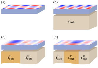
So far, two-dimensional (2D) plasmonic devices have been manufactured either by strongly invasive processes, such as structuring the activate material itself [26, 27, 28, 29, 30], by changes to the single-particle properties of the plasmon-hosting system [31, 32, 33, 34], or by creating metallic heterostructures [35]. Here, we propose a truly non-invasive concept based on the external control of the Coulomb interactions within the active material. Specifically, we show how 2D plasmons in an homogeneous layered material can be spatially controlled with the help of structured dielectric environments, as depicted in Fig. 1. An analogous Coulomb engineering concept has been previously applied to atomically thin semiconductors [36, 37, 38, 39, 40, 41, 42, 43]. Here, we apply this concept to active metallic systems. Specifically, we will consider homogeneous as well as horizontally staggered dielectric environments. By realistically accounting for horizontal and vertical dielectric-interface effects via image charge models within a real space random phase approximation, we show that plasmons can be precisely confined at certain optimal excitation energies. This allows for the non-invasive creation of plasmonic waveguides, as illustrated in Fig. 1 (d), whereby the active, plasmon hosting, monolayer remains unchanged.
II Results and Discussion
II.1 Substrate Controlled 2D Plasmons
In the following, we describe the plasmonic excitations in layered metals using a single-orbital generalized Hubbard model of the form
| (1) | ||||
where () creates (annihilates) an electron of spin at the square-lattice site , are the corresponding occupation operators, eV is the nearest neighbour hopping, and is the non-local Coulomb interaction. We fix the Fermi energy to and treat the model within the random phase approximation. To realistically describe the collective excitations of a generic layered metal in terms of this model we need to account for all involved screening channels. This includes intra- and inter-band polarizations within the layered material itself [22, 21, 20], as well as external polarization effects from the environment, such as substrates or capping layers. To this end we consider the fully screened Coulomb interaction in the metallic film for in-plane momentum transfer ,
| (2) |
where , , and are the total polarization, the dielectric function, and the bare Coulomb interaction, respectively. By splitting into the metallic polarization, resulting from intra-band transitions within the active layered material itself described by the Hamiltonian above, and a residual polarization, accounting for inter-band transitions and substrate screening, we can rewrite the fully screened Coulomb interaction as
| (3) |
where is the Fourier transform of accounting for the residual screening channels. The full dielectric function is thus given by the product . We calculate within the Random Phase Approximation (RPA) based on the Hamilton from above and by neglecting local-field effects, while the residual screening can be analytically approximated from classical electrostatics, which reads for a layered material of effective height and intrinsic dielectric constant [44, 45, 21, 36]
| (4) |
For a dielectric encapsulation, as shown in Fig. 2 (b), we find . This allows us to define the electron energy loss spectrum (EELS),
| (5) |
According to the implicit definition of plasmonic excitations, , the electron energy loss spectrum is maximized along the plasmonic dispersion . This way, we can extract along a path in momentum space, shown in Fig. 2 (d), along with the metallic polarization function . The model parameters are chosen to approximately reproduce the plasmonic energy scales of metallic transition metal dichalcogenides [21, 44, 22] and doped hexagonal boron nitride [46]. We observe that even in the free-standing case () the plasmonic dispersion deviates quickly from the generic -like dispersion [22, 21, 20], known from purely two-dimensional models. This deviation is a consequence of the non-local residual screening induced by inter-band transitions within the layered metal, which we plot in Fig. 2 (a).
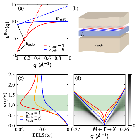
For the free-standing case, its long and short wavelength limits are and , respectively. Hence, in the long wavelength limit the effective background screening is negligible [47], and holds. For larger momenta, however, increases successively, which suppresses and eventually pushes it into the particle-hole continuum. Importantly, the corresponding flattening of the plasmonic dispersion takes place at momenta which are clearly detached from the particle-hole continuum, so that Landau damping and thus plasmonic losses are drastically reduced in layered metals at small and intermediate momenta [20, 46, 22, 21]. This, in turn, leads to a prominent enhancement of the plasmonic spectral function at intermediate frequencies, as it is clearly visible in the , shown in Fig. 2 (c) (green shaded region). Upon increasing the environmental screening, e.g. by using different substrate materials [illustrated in Fig. 2 (b)], the long wavelength limit of the effective residual screening is changed to . This leads to a decreased , and subsequently to a reduced plasmonic dispersion with enhanced slopes for small momenta. In the full we correspondingly find a decreased and broadened maximum at intermediate frequencies, whereas the remainder of the plasmonic spectrum is largely unaffected. This intermediate frequency range in the plasmonic spectral function is thus most susceptible to changes in the environmental screening of the layered material.
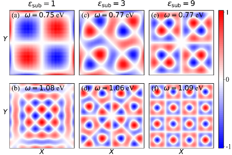
The enhanced environmental screening sensitivity of plasmons in layered materials at intermediate excitation energies is also reflected in the corresponding real space charge density patterns, shown in Figs. 3 (a-f) at eV and eV for the same as before. Here, we observe extended modes with checkerboard-like patterns oscillating along the and directions. At a fixed excitation energy, these patterns show decreasing wavelengths upon increasing the environmental screening, in line with the corresponding dispersions shown in Fig. 2 (d). Similarly, we observe that the plasmonic wavelengths decrease with increasing excitation energies at fixed screening.
This demonstrates how spatial patterns of 2D plasmons can be controlled by means of dielectric substrates. In the following, we illustrate how this can be utilized to spatially confine plasmonic excitations by using structured dielectric environments.
II.2 2D Plasmons in Heterogeneous Screening Environments
Let us now consider a heterogeneous dielectric environment with a vertical interface separating areas with and , as depicted in Fig. 4 (a). Since this breaks the translational symmetry along the -direction, we are forced to switch to a real space representation. To this end, we utilize a supercell consisting of unit cells. In Fig. 4 (c) we show the resulting heterogeneous EELS (black) as well as the corresponding EELS for the two homogeneous situations (red and blue). By comparing the heterogeneous spectrum to the unsupported one (i.e. ), we observe that the maximum at intermediate excitation energies (green shaded) is still present, but suppressed. Furthermore, we see that at low energies (yellow shaded) a new shoulder arises, which aligns with the onset of the spectral function of a homogeneously supported monolayer with . The heterogeneous spectral function thus clearly inherits characteristics from both homogeneous limits. The origin of this becomes obvious by examining the corresponding real space charge modulations. At small excitation energies, the plasmons are mostly localized in the region, as seen in Fig. 4 (d), whereas at intermediate excitation energies they prominently reside in the area, as observed in Figs. 4 (e-g).
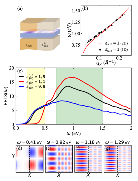
This illustrates how heterogeneous plasmonic patterns can be externally and non-invasively induced in homogeneous layered materials via spatially structured substrates. The substrate induced heterogeneous plasmonic patterns behave, however, slightly differently compared to their homogeneous counterparts depicted in Fig. 3. For intermediate excitation energies, which mostly confine the plasmon in the region, the resulting pattern is now quasi-one-dimensional. Specifically, we observe that its propagation direction aligns with the dielectric interface in the substrate and has a linear dispersion, as shown in Fig. 4 (b). Additionally, there are some spurious, strongly damped, plasmonic excitations present in the region.
Interestingly, the fully heterogeneous EELS [black line in Fig. 4 (c)] can be approximately reconstructed by taking a simple average over the homogeneous data (blue and red lines). From this we understand that the environement barely affects the low-energy plasmonic excitations confined in the area, which does not hold vice versa. I.e. the slightly damps the plasmonic excitations on the side. However, except from this, these two patterns behave largely independently on the other side.
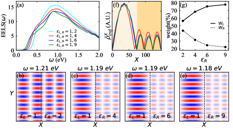
We proceed with a quantitative analysis of these confined excitations by investigating their dependence on the dielectric contrast ratio in the substrate. To this end, we fix and vary . In Fig. 5 (a) we observe that increasing the contrast affects the EELS in a non-trivial way. At small dielectric contrasts, the full heterogeneous EELS resembles a homogeneous one, with just one broad maximum at intermediate excitation energies, which is reflected in the rather spread-out plasmonic excitation pattern depicted in Fig. 5 (b). Upon increasing the substrate dielectric contrast, we find a low-energy energy shoulder arising and shifting to lower frequencies. However, overall we find an increasing localization of the plasmonic pattern on the side, with decreasing weight on the side for eV, as depicted in Figs. 5 (c-e). We can furthermore quantify this increasing localization with the help of the normalized charge distribution function, , obtained by integrating the absolute value of the real space charge distribution function along the -component [see Fig. 5 (f)]. By additionally integrating over the left and right regions we can define sub-space weights , which we show in Fig. 5 (g). Then we observe that up to nearly of the charge can be confined within the left region for the maximum dielectric contrast considered here. As a result the plasmonic excitation in the area gets relatively brighter. However, increasing also damps the excitation in the region. Therefore, achieving an optimal dielectric contrast will be a trade-off between spatial contrast and brightness of the plasmons on the active side. Finally, we note that the -confined quasi-one-dimensional plasmon wavelength is not affected by .
II.3 Novel Plasmonic Waveguides
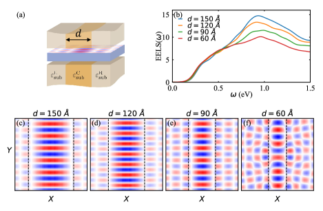
The possibility to non-invasively spatially pattern plasmonic excitations in a homogeneous layered material by means of dielectric interfaces in the dielectric environment motivates us to propose a new class of plasmonic waveguides that utilizes two parallel vertical dielectric interfaces in the environment, as illustrated in Fig. 6 (a). This will confine well-defined quasi-one-dimensional plasmons in the central region if the substrate’s dielectric constant there is smaller than in the outer substrate regions. To verify this proposal, we study below a system with and , and with variable central substrate width .
In Fig. 6 (a) we show the EELS for various . Starting from large , we recover the previously discussed maximum at intermediate excitation energies which is accompanied by a low-energy shoulder. Upon decreasing , this maximum diminishes until it vanishes below Å ( unit cells). This behavior becomes clear by examining the corresponding real space patterns shown in Figs. 6 (c-f). Fig. 6 (c) reveals that the plasmon mode is now indeed spatially confined in the central substrate area and propagates only parallel to the substrate dielectric interfaces. Thus, the maximum in EELS results from the low-dielectric substrate region, and the correspondingly confined plasmonic excitation there. Upon decreasing , we observe in Figs. 6 (d-f) that the novel plasmonic waveguide behavior persists, but with gradually decreasing contrast to the areas, until it nearly vanishes for the smallest shown in Fig. 6 (f). Thus, the increasing environmental screening from the increasing regions gradually damps the confined excitation in the center of the device until no spatial structure is visible anymore. Nevertheless, a clear confinement can be achieved for waveguides with widths down to about unit cells, which is on the order of Å here. Like in the case of the dielectric contrast, there is a trade-off between the field confinement and loss in the optimization of these plasmonic waveguides [19, 48]. This is a demonstration of a novel type of plasmonic waveguides, based on Coulomb-engineered homogeneous layered metallic materials.
III Outlook and Conclusions
Active Material Candidates: Apart from the properties of the structured dielectric environment, our proposal also depends strongly on the active material itself, i.e. not all 2D metals will be equally suitable. Specifically, the active metallic layer should be very sensitive to environmental screening. This is the case if all layer-internal polarization channels (intra- and inter-band) are rather small, in other words: materials with a small density of states at the Fermi level and with a metallic (low-energy plasmon hosting) band which is energetically well separated from all other valence and conduction bands. Both of these properties are satisfied in graphene: it hosts low-loss plasmons [49, 50, 28, 51, 52], and the Coulomb interactions have been experimentally shown to be rather susceptible to external polarization [47, 53, 35]. Alternatively, slightly doped semi-conducting layered materials, such as electron or hole doped MoS2 or WS2, could be suitable candidates due to reduced intra-band polarization as well as metallic -NbS2 and -AlCl2 due to their low internal plasmonic losses [44].
Structured Environments: For the creation of structured environments, as needed for the proposed waveguides, we envision laterally grown and vertically cut lithographic structures, twisted layered materials [54, 55, 56], or novel fractionalized 2D system [57, 58, 59] to be possible routes to pursue. As discussed above, the dielectric contrast in these structures should be rather high. Furthermore, it will be interesting to create environmental screening structures with more than just one or two dielectric interfaces. One could, for example, imagine periodically patterned substrates for optimal light-matter coupling, two-dimensional dielectric structures that either create plasmonic checkerboard patterns or plasmonic quantum dots, or non-linear plasmonic waveguides [60].
Conclusions: Our generic model calculations suggest that it is feasible to externally functionalize a homogeneous 2D metallic layer by means of structured dielectric environments, thus creating new plasmonic waveguides using existing experimental techniques and available layered materials. In contrast to previous functionalization concepts, our approach only relies on a passive pre-structured environment, to which the active layer needs to be exposed. Depending on the spatially modulated dielectric contrast in this environment plasmons can be confined within a nm scale. At the same time, the described optimal excitation energy window for our proposal renders these devices highly specific to external stimuli allowing for switching or filtering applications. The optimization of these new plasmonic devices will thereby be a trade-off between the plasmonic localization and relative brightness which is controlled by the dielectric contrast in the heterogeneous environment.
Furthermore, we highlight that the described induced plasmonic functionality relies on spatial structuring of the dynamically screened Coulomb interaction within the material. Thus, it can also affect a variety of other many-body properties, including many-body excitations, such as magnons, and many-body instabilities, such as superconductivity or magnetism. The proposed plasmonic waveguide is therefore just one possible example of a more general concept for Coulomb-engineering of many-body properties in metallic layered materials with a variety of further applications.
Acknowledgements.
The authors thank Frank Koppens, Mikhail I. Katsnelson, and Henning Schlömer for useful discussions. This work was supported by the US Department of Energy under grant number DE-FG02-05ER46240. The numerical computations were carried out on the University of Southern California High Performance Supercomputer Cluster.Appendix A Background Screening Model
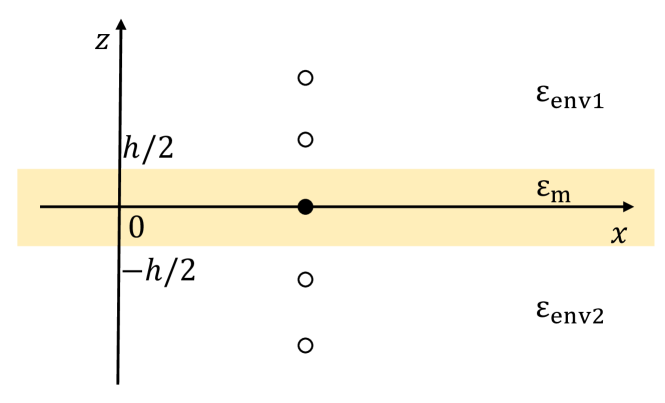
In vacuum the Coulomb interaction between two point charges and is simply given by , where is the distance between them. In the case of electrons within a realistic material the effective interaction between them is more complicated due to the polarizable environment [20, 21, 61, 62]. In layered materials, this internal “background” screening can be classically well approximated by a dielectric-slab model. As illustrated in Fig. 7, the electrons are supposed to be confined in the center () plane of the dielectric slab, which is defined by the effective height and the dielectric constant . These two parameters are determined from the intrinsic properties of the 2D material and can be calculated from first-principles [61, 36, 21]. Here we set Å and similar to the situation in transition mental dichalcogenide monolayers [37]. and are the environmental dielectric constants above and below the 2D material.
The “background” screened Coulomb interaction between two electrons in the plane with a separation can then be determined using an iterated image-charge ansatz [45, 63, 64]. The image charges (empty circles) generated by the real charge (solid circle) are shown in Fig. 7. In principle, there is an infinite number of image charges along the -direction and their charges are determined by , , and . The full “background” screened Coulomb interaction on the plane is given by the sum of all of these contributions. Here, we consider . Then, is given by
| (6) |
where and . The first term in Eq. (6) is the contribution from the real (source) charge, whereas the second term results from the image charges.
For the on-site interaction, i.e. , the above formula diverges. To avoid this, we define the “on-site” interaction at a slightly shifted position with a small separation above the source charge itself. In the numerical calculation we set Å, which yields the on-site Coulomb energy to be for the unsupported layer.
Appendix B Image Charge Ansatz for Spatially Structured Substrates
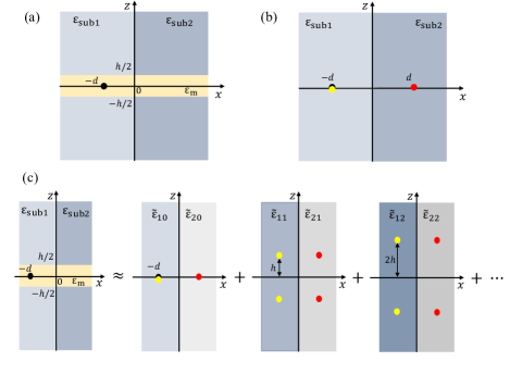
As soon as we additionally introduce vertical dielectric interfaces in the screening environment, the effective Coulomb interaction for can analytically only be approximately described. The configuration with a single vertical interface is illustrated in Fig. 8 (a). In the following we put a real charge (solid circle) on the plane at a distance of to the vertical interface. The aim is to approximate the Coulomb potential on the full plane from this point charge.
To this end we combine the analytically known solutions for the homogeneous dielectric slab (two parallel horizontal dielectric interfaces) with the homogeneous single dielectric interface situation depicted in Fig. 8 (b). In the latter case the analytically correct potential can be constructed using a single additional image charge. In detail, if we place our source charge at [black dot in Fig. 8 (b)] we will need an additional image charge at . For this yields
| (7) |
with , and . For we correspondingly get
| (8) |
with and . This method is discussed in many text books and we refer the interested reader, e.g., to Ref. 63.
The Coulomb interaction on the plane, before introducing the vertical interface, is already discussed in Appendix A and given by Eq. (6), which we can slightly reformulate to
| (9) |
In this way, we can interpret as the Coulomb interaction between an electron at with a series of (electron) point charges positioned at which are each embedded in different homogeneous dielectric backgrounds .
Now, to model the effect of the additional vertical dielectric interface (between and ), we just need to introduce vertical image charges for each of these iterated horizontal image charge as described in Eqs. (7, 7) and illustrated in Fig. 8. The full approximate interactions can thus be written as a summation of the form
| (10) |
where each is evaluated as in the simple image charge method introduced before, however, with adjusted parameters. Specifically we need to replace and by and to evaluate and , and replace by , by and by . Altogether we get
| (11) |
When two parallel vertical interfaces are introduced in the dielectric background, i.e. like the plasmonic waveguide configuration introduced in the main text, we use the same concept. Now, however, we also need to introduce an infinite series of iterated image charges in -direction.
Appendix C Plasmonic Excitations in Real Space
We aim to analyze the dielectric function
| (12) |
in real space. To this end we use the Coulomb interaction models from appendix A and B and evaluate the bare polarization of the metallic band within the random phase approximation. Since the the active metallic layer itself is translational invariant we can start in momentum space:
| (13) |
with being the non-interacting single-particle metallic-band dispersion at , the corresponding Fermi function, and eV a finite broadening. The real-space representation in the atomic basis can then be obtained via an inverse Fourier transformation [65],
| (14) |
Here, the vectors are defined on the real-space lattice. This two-step calculation greatly improves the computational efficiency. Finally, we obtain the real-space dielectric function as a matrix in the atomic basis via
| (15) |
The plasmonic excitations are identified from a spectral decomposition of the dielectric matrix,
| (16) |
by selecting the “leading” dielectric eigenvalue which maximizes the electron energy loss spectrum together with its eigenvector for each frequency. The real-space charge modulation of a plasmon mode at the frequency can be obtained from
| (17) |
[66]. Here, we interpret the “leading” eigenvector as the total potential distribution at the plasmon frequency , since it solves the equation
| (18) |
when , namely
| (19) |
i.e. for . The product then represents the induced charge distribution in the system. The full method has been reported in previous studies [67, 57, 68]. Finally, we note that by restricting the continuous position coordinates and to the discretized lattice positions and we effectively neglect local-field effects [65].
References
- Hedin [1965] L. Hedin, New method for calculating the one-particle Green’s function with application to the electron-gas problem, Physical Review 139, A796 (1965).
- Aryasetiawan and Gunnarsson [1998] F. Aryasetiawan and O. Gunnarsson, The GW method, Reports on Progress in Physics 61, 237 (1998).
- Onida et al. [2002] G. Onida, L. Reining, and A. Rubio, Electronic excitations: Density-functional versus many-body Green’s-function approaches (2002).
- Kas et al. [2014] J. J. Kas, J. J. Rehr, and L. Reining, Cumulant expansion of the retarded one-electron Green function, Physical Review B 90, 085112 (2014).
- Steinhoff et al. [2017] A. Steinhoff, M. Florian, M. Rösner, G. Schönhoff, T. O. Wehling, and F. Jahnke, Exciton fission in monolayer transition metal dichalcogenide semiconductors, Nature Communications 8, 1 (2017).
- Barnes et al. [2003] W. L. Barnes, A. Dereux, and T. W. Ebbesen, Surface plasmon subwavelength optics (2003).
- Low et al. [2017] T. Low, A. Chaves, J. D. Caldwell, A. Kumar, N. X. Fang, P. Avouris, T. F. Heinz, F. Guinea, L. Martin-Moreno, and F. Koppens, Polaritons in layered two-dimensional materials (2017).
- Bill et al. [2003] A. Bill, H. Morawitz, and Z. Kresin, Electronic collective modes and superconductivity in layered conductors, Physical Review B 68, 144519 (2003).
- Hepting et al. [2018] M. Hepting, L. Chaix, E. W. Huang, R. Fumagalli, Y. Y. Peng, B. Moritz, K. Kummer, N. B. Brookes, W. C. Lee, M. Hashimoto, T. Sarkar, J. F. He, C. R. Rotundu, Y. S. Lee, R. L. Greene, L. Braicovich, G. Ghiringhelli, Z. X. Shen, T. P. Devereaux, and W. S. Lee, Three-dimensional collective charge excitations in electron-doped copper oxide superconductors, Nature 563, 374 (2018).
- Van Wezel et al. [2011] J. Van Wezel, R. Schuster, A. König, M. Knupfer, J. Van Den Brink, H. Berger, and B. Büchner, Effect of charge order on the plasmon dispersion in transition-metal dichalcogenides, Physical Review Letters 107, 176404 (2011).
- Kogar et al. [2017] A. Kogar, M. S. Rak, S. Vig, A. A. Husain, F. Flicker, Y. I. Joe, L. Venema, G. J. MacDougall, T. C. Chiang, E. Fradkin, J. Van Wezel, and P. Abbamonte, Signatures of exciton condensation in a transition metal dichalcogenide, Science 358, 1314 (2017).
- Oulton et al. [2008] R. F. Oulton, V. J. Sorger, D. A. Genov, D. F. Pile, and X. Zhang, A hybrid plasmonic waveguide for subwavelength confinement and long-range propagation, Nature Photonics 2, 496 (2008).
- Ansell et al. [2015] D. Ansell, I. P. Radko, Z. Han, F. J. Rodriguez, S. I. Bozhevolnyi, and A. N. Grigorenko, Hybrid graphene plasmonic waveguide modulators, Nature Communications 6, 1 (2015).
- Fang and Sun [2015] Y. Fang and M. Sun, Nanoplasmonic waveguides: Towards applications in integrated nanophotonic circuits (2015).
- Ditlbacher et al. [2005] H. Ditlbacher, A. Hohenau, D. Wagner, U. Kreibig, M. Rogers, F. Hofer, F. R. Aussenegg, and J. R. Krenn, Silver nanowires as surface plasmon resonators, Physical Review Letters 95, 257403 (2005).
- Bozhevolnyi et al. [2006] S. I. Bozhevolnyi, V. S. Volkov, E. Devaux, J. Y. Laluet, and T. W. Ebbesen, Channel plasmon subwavelength waveguide components including interferometers and ring resonators, Nature 440, 508 (2006).
- Schnell et al. [2011] M. Schnell, P. Alonso-González, L. Arzubiaga, F. Casanova, L. E. Hueso, A. Chuvilin, and R. Hillenbrand, Nanofocusing of mid-infrared energy with tapered transmission lines, Nature Photonics 5, 283 (2011).
- Boltasseva et al. [2008] A. Boltasseva, V. S. Volkov, R. B. Nielsen, E. Moreno, S. G. Rodrigo, and S. I. Bozhevolnyi, Triangular metal wedges for subwavelength plasmon-polariton guiding at telecom wavelengths, Optics Express 16, 5252 (2008).
- Kress et al. [2015] S. J. Kress, F. V. Antolinez, P. Richner, S. V. Jayanti, D. K. Kim, F. Prins, A. Riedinger, M. P. Fischer, S. Meyer, K. M. McPeak, D. Poulikakos, and D. J. Norris, Wedge Waveguides and Resonators for Quantum Plasmonics, Nano Letters 15, 6267 (2015).
- da Jornada et al. [2020] F. H. da Jornada, L. Xian, A. Rubio, and S. G. Louie, Universal slow plasmons and giant field enhancement in atomically thin quasi-two-dimensional metals, Nature Communications 11, 1 (2020).
- Groenewald et al. [2016] R. E. Groenewald, M. Rösner, G. Schönhoff, S. Haas, and T. O. Wehling, Valley plasmonics in transition metal dichalcogenides, Physical Review B 93, 205145 (2016).
- Andersen and Thygesen [2013] K. Andersen and K. S. Thygesen, Plasmons in metallic monolayer and bilayer transition metal dichalcogenides, Physical Review B 88, 155128 (2013).
- Liu et al. [2008] Y. Liu, R. F. Willis, K. V. Emtsev, and T. Seyller, Plasmon dispersion and damping in electrically isolated two-dimensional charge sheets, Physical Review B 78, 201403 (2008).
- Gjerding et al. [2017] M. N. Gjerding, M. Pandey, and K. S. Thygesen, Band structure engineered layered metals for low-loss plasmonics, Nature Communications 8, 1 (2017).
- Woessner et al. [2015] A. Woessner, M. B. Lundeberg, Y. Gao, A. Principi, P. Alonso-González, M. Carrega, K. Watanabe, T. Taniguchi, G. Vignale, M. Polini, J. Hone, R. Hillenbrand, and F. H. Koppens, Highly confined low-loss plasmons in graphene-boron nitride heterostructures, Nature Materials 14, 421 (2015).
- Nikitin et al. [2011] A. Y. Nikitin, F. Guinea, F. J. García-Vidal, and L. Martín-Moreno, Edge and waveguide terahertz surface plasmon modes in graphene microribbons, Physical Review B 84, 161407 (2011).
- Yuan et al. [2013] S. Yuan, F. Jin, R. Roldán, A. P. Jauho, and M. I. Katsnelson, Screening and collective modes in disordered graphene antidot lattices, Physical Review B 88, 195401 (2013).
- Christensen et al. [2012] J. Christensen, A. Manjavacas, S. Thongrattanasiri, F. H. Koppens, and F. J. García De Abajo, Graphene plasmon waveguiding and hybridization in individual and paired nanoribbons, ACS Nano 6, 431 (2012).
- Kim and Choi [2011] J. T. Kim and S.-Y. Choi, Graphene-based plasmonic waveguides for photonic integrated circuits, Optics Express 19, 24557 (2011).
- Thongrattanasiri et al. [2012] S. Thongrattanasiri, F. H. Koppens, and F. J. García De Abajo, Complete optical absorption in periodically patterned graphene, Physical Review Letters 108, 047401 (2012).
- Vakil and Engheta [2011] A. Vakil and N. Engheta, Transformation optics using graphene, Science 332, 1291 (2011).
- Liu et al. [2011] M. Liu, X. Yin, E. Ulin-Avila, B. Geng, T. Zentgraf, L. Ju, F. Wang, and X. Zhang, A graphene-based broadband optical modulator, Nature 474, 64 (2011).
- Prishchenko et al. [2018] D. A. Prishchenko, V. G. Mazurenko, M. I. Katsnelson, and A. N. Rudenko, Gate-tunable infrared plasmons in electron-doped single-layer antimony, Physical Review B 98, 201401 (2018).
- Slotman et al. [2018] G. Slotman, A. Rudenko, E. Van Veen, M. I. Katsnelson, R. Roldán, and S. Yuan, Plasmon spectrum of single-layer antimonene, Physical Review B 98, 155411 (2018).
- Iranzo et al. [2018] D. A. Iranzo, S. Nanot, E. J. Dias, I. Epstein, C. Peng, D. K. Efetov, M. B. Lundeberg, R. Parret, J. Osmond, J. Y. Hong, J. Kong, D. R. Englund, N. M. Peres, and F. H. Koppens, Probing the ultimate plasmon confinement limits with a van der Waals heterostructure, Science 360, 291 (2018).
- Rösner et al. [2016] M. Rösner, C. Steinke, M. Lorke, C. Gies, F. Jahnke, and T. O. Wehling, Two-Dimensional Heterojunctions from Nonlocal Manipulations of the Interactions, Nano Letters 16, 2322 (2016).
- Steinke et al. [2020] C. Steinke, T. O. Wehling, and M. Rösner, Coulomb-engineered heterojunctions and dynamical screening in transition metal dichalcogenide monolayers, Physical Review B 102, 115111 (2020).
- Raja et al. [2017] A. Raja, A. Chaves, J. Yu, G. Arefe, H. M. Hill, A. F. Rigosi, T. C. Berkelbach, P. Nagler, C. Schüller, T. Korn, C. Nuckolls, J. Hone, L. E. Brus, T. F. Heinz, D. R. Reichman, and A. Chernikov, Coulomb engineering of the bandgap and excitons in two-dimensional materials, Nature Communications 8, 1 (2017).
- Florian et al. [2018] M. Florian, M. Hartmann, A. Steinhoff, J. Klein, A. W. Holleitner, J. J. Finley, T. O. Wehling, M. Kaniber, and C. Gies, The Dielectric Impact of Layer Distances on Exciton and Trion Binding Energies in van der Waals Heterostructures, Nano Letters 18, 2725 (2018).
- Steinleitner et al. [2018] P. Steinleitner, P. Merkl, A. Graf, P. Nagler, K. Watanabe, T. Taniguchi, J. Zipfel, C. Schüller, T. Korn, A. Chernikov, S. Brem, M. Selig, G. Berghäuser, E. Malic, and R. Huber, Dielectric Engineering of Electronic Correlations in a van der Waals Heterostructure, Nano Letters 18, 1402 (2018).
- van Loon et al. [2020] E. G. C. P. van Loon, M. Schüler, D. Springer, G. Sangiovanni, J. M. Tomczak, and T. O. Wehling, Coulomb Engineering of two-dimensional Mott materials, arXiv (2020), arXiv:2001.01735 .
- Utama et al. [2019] M. I. B. Utama, H. Kleemann, W. Zhao, C. S. Ong, F. H. da Jornada, D. Y. Qiu, H. Cai, H. Li, R. Kou, S. Zhao, S. Wang, K. Watanabe, T. Taniguchi, S. Tongay, A. Zettl, S. G. Louie, and F. Wang, A dielectric-defined lateral heterojunction in a monolayer semiconductor, Nature Electronics 2, 60 (2019).
- Kajino et al. [2019] Y. Kajino, K. Oto, and Y. Yamada, Modification of Optical Properties in Monolayer WS2 on Dielectric Substrates by Coulomb Engineering, Journal of Physical Chemistry C 123, 14097 (2019).
- Andersen et al. [2015] K. Andersen, S. Latini, and K. S. Thygesen, Dielectric Genome of van der Waals Heterostructures, Nano Letters 15, 4616 (2015), arXiv:1506.02463 .
- Cho and Berkelbach [2018] Y. Cho and T. C. Berkelbach, Environmentally sensitive theory of electronic and optical transitions in atomically thin semiconductors, Physical Review B 97, 041409 (2018), arXiv:1709.01094 .
- Lončarić et al. [2018] I. Lončarić, Z. Rukelj, V. M. Silkin, and V. Despoja, Strong two-dimensional plasmon in Li-intercalated hexagonal boron-nitride film with low damping, npj 2D Materials and Applications 2, 33 (2018).
- Lundeberg et al. [2017] M. B. Lundeberg, Y. Gao, R. Asgari, C. Tan, B. V. Duppen, M. Autore, P. Alonso-González, A. Woessner, K. Watanabe, T. Taniguchi, R. Hillenbrand, J. Hone, M. Polini, and F. H. Koppens, Tuning quantum nonlocal effects in graphene plasmonics, Science 357, 187 (2017).
- Tame et al. [2013] M. S. Tame, K. R. McEnery, . K. Özdemir, J. Lee, S. A. Maier, and M. S. Kim, Quantum plasmonics (2013).
- Jablan et al. [2009] M. Jablan, H. Buljan, and M. Soljačić, Plasmonics in graphene at infrared frequencies, Physical Review B 80, 245435 (2009).
- Low and Avouris [2014] T. Low and P. Avouris, Graphene plasmonics for terahertz to mid-infrared applications (2014).
- Grigorenko et al. [2012] A. N. Grigorenko, M. Polini, and K. S. Novoselov, Graphene plasmonics (2012).
- Luo et al. [2013] X. Luo, T. Qiu, W. Lu, and Z. Ni, Plasmons in graphene: Recent progress and applications (2013).
- Kim et al. [2020] M. Kim, S. G. Xu, A. I. Berdyugin, A. Principi, S. Slizovskiy, N. Xin, P. Kumaravadivel, W. Kuang, M. Hamer, R. Krishna Kumar, R. V. Gorbachev, K. Watanabe, T. Taniguchi, I. V. Grigorieva, V. I. Fal’ko, M. Polini, and A. K. Geim, Control of electron-electron interaction in graphene by proximity screenings, Nature Communications 11, 1 (2020).
- Bistritzer and MacDonald [2011] R. Bistritzer and A. H. MacDonald, Moiré bands in twisted double-layer graphene, Proceedings of the National Academy of Sciences of the United States of America 108, 12233 (2011).
- Andrei and MacDonald [2020] E. Y. Andrei and A. H. MacDonald, Graphene bilayers with a twist, Nature Materials 19, 1265 (2020).
- Weston et al. [2020] A. Weston, Y. Zou, V. Enaldiev, A. Summerfield, N. Clark, V. Zólyomi, A. Graham, C. Yelgel, S. Magorrian, M. Zhou, J. Zultak, D. Hopkinson, A. Barinov, T. H. Bointon, A. Kretinin, N. R. Wilson, P. H. Beton, V. I. Fal’ko, S. J. Haigh, and R. Gorbachev, Atomic reconstruction in twisted bilayers of transition metal dichalcogenides, Nature Nanotechnology 15, 592 (2020).
- Westerhout et al. [2018] T. Westerhout, E. Van Veen, M. I. Katsnelson, and S. Yuan, Plasmon confinement in fractal quantum systems, Physical Review B 97, 205434 (2018).
- He et al. [2019] T. He, Z. Wang, F. Zhong, H. Fang, P. Wang, and W. Hu, Etching Techniques in 2D Materials, Advanced Materials Technologies 4, 1900064 (2019).
- De Nicola et al. [2020] F. De Nicola, N. S. Puthiya Purayil, V. Miŝeikis, D. Spirito, A. Tomadin, C. Coletti, M. Polini, R. Krahne, and V. Pellegrini, Graphene Plasmonic Fractal Metamaterials for Broadband Photodetectors, Scientific Reports 10, 17 (2020).
- Sahoo et al. [2018] P. K. Sahoo, S. Memaran, Y. Xin, L. Balicas, and H. R. Gutiérrez, One-pot growth of two-dimensional lateral heterostructures via sequential edge-epitaxy, Nature 553, 63 (2018).
- Rösner et al. [2015] M. Rösner, E. Şaşloʇlu, C. Friedrich, S. Blügel, and T. O. Wehling, Wannier function approach to realistic Coulomb interactions in layered materials and heterostructures, Physical Review B 92, 085102 (2015).
- Rösner et al. [2018] M. Rösner, R. E. Groenewald, G. Schönhoff, J. Berges, S. Haas, and T. O. Wehling, Plasmonic Superconductivity in Layered Materials, arXiv (2018), arXiv:1803.04576 .
- Jackson and Fox [1999] J. D. Jackson and R. F. Fox, Classical Electrodynamics, 3rd ed . , American Journal of Physics 67, 841 (1999).
- Kumagai and Takagahara [1989] M. Kumagai and T. Takagahara, Excitonic and nonlinear-optical properties of dielectric quantum-well structures, Physical Review B 40, 12359 (1989).
- Van Schilfgaarde and Katsnelson [2011] M. Van Schilfgaarde and M. I. Katsnelson, First-principles theory of nonlocal screening in graphene, Physical Review B 83, 081409 (2011).
- Fahimniya et al. [2020] A. Fahimniya, C. Lewandowski, and L. Levitov, Dipole-active collective excitations in moiré flat bands, arXiv (2020), arXiv:2011.02982 .
- Wang et al. [2015] W. Wang, T. Christensen, A. P. Jauho, K. S. Thygesen, M. Wubs, and N. A. Mortensen, Plasmonic eigenmodes in individual and bow-tie graphene nanotriangles, Scientific Reports 5, 1 (2015).
- Jiang et al. [2020] Z. Jiang, M. Rösner, R. E. Groenewald, and S. Haas, Localized plasmons in topological insulators, Physical Review B 101, 045106 (2020).