Tuning the mode-splitting of a semiconductor microcavity with uniaxial stress
Abstract
A splitting of the fundamental optical modes in micro/nano-cavities comprising semiconductor heterostructures is commonly observed. Given that this splitting plays an important role for the light-matter interaction and hence quantum technology applications, a method for controlling the mode-splitting is important. In this work we use an open microcavity composed of a “bottom” semiconductor distributed Bragg reflector (DBR) incorporating an n-i-p heterostructure, paired with a “top” curved dielectric DBR. We measure the mode-splitting as a function of wavelength across the stopband. We demonstrate a reversible in-situ technique to tune the mode-splitting by applying uniaxial stress to the semiconductor DBR. The method exploits the photoelastic effect of the semiconductor materials. We achieve a maximum tuning of 11 GHz. The stress applied to the heterostructure is determined by observing the photoluminescence of quantum dots embedded in the sample, converting a spectral shift to a stress via deformation potentials. A thorough study of the mode-splitting and its tuning across the stop-band leads to a quantitative understanding of the mechanism behind the results.
Semiconductor quantum dots (QDs) coupled to optical microcavities represent an important platform to advance quantum information technologies. Semiconductor QD-cavity platforms, such as micropillars, photonic crystals and open microcavities, have been successfully employed to achieve highly efficient single-photon sources Wang et al. (2019); Tomm et al. (2021), a coherent light-matter interaction (Najer et al., 2019), generation of entangled photons Dousse et al. (2010); Liu et al. (2019), and photon-photon switches Fushman et al. (2008). Despite the history of successful cavity quantum-electrodynamics demonstrations in these systems, there are still partly unresolved technical questions that affect their performance. One such property is the almost ubiquitous observation that the fundamental cavity mode splits into two separate modes with linear, orthogonal polarizations. This lifting of the polarization degeneracy is desired and exploited in some cases, notably in efficient single-photon sources in order to avoid a 50% loss of signal in cross-polarized collection schemes Wang et al. (2019); Tomm et al. (2021). In this scenario, a QD trion is excited via one cavity mode, and photons are preferentially emitted into the other cavity mode. In other cases however, polarization degenerate cavity modes are desirable. This is typically the case in experiments relying on circularly polarized excitation schemes Lodahl et al. (2017), for instance a single spin in a perpendicular magnetic field. Here, the linearly polarized cavity modes result in a reduced coupling to the quantum emitter Söllner et al. (2015). It is not simple to control the bare mode-splitting precisely – it can depend on the local inbuilt strain in the material, and on fabrication imperfections. For all these reasons, a way of selectively tuning and controlling the mode-splitting is of great interest.
The polarization splitting of a semiconductor microcavity’s fundamental mode is the result of birefringence in the semiconductor between two orthogonal crystalline axes (which are themselves orthogonal to the optical axis). In zinc-blende type crystals there is a priori no intrinsic birefringence. Birefringence can be created however, often unintentionally, via two mechanisms. First, in heterostructures incorporating a diode or Schottky structure, the in-built electric field along the direction (growth axis) breaks the inversion symmetry of the crystal and birefringence in the - plane arises via the linear electro optic effect van Exter, Jansen van Doorn, and Woerdman (1997). Secondly, a uniaxial stress in the - plane, induced by microscopic imperfections in the heterostructure or post-growth processing, induces birefringence via the photoelastic effect van der Ziel and Gossard (1977); Raynolds, Levine, and Wilkins (1995). Contrarily, a biaxial stress does not result in observable birefringence on account of the symmetry of the zinc-blende crystal.
One can use the electrooptic and photoelastic effects to reverse or enhance the birefringence in semiconductor cavities, as previously demonstrated in monolithic structures Bonato et al. (2009); Frey et al. (2018); Gerhardt et al. (2020). Here, we present a way of tuning the mode-splitting of an open microcavity by making use of the photoelastic effect, i.e. the control of the birefringence upon application of uniaxial stress. A change in mode-splitting of GHz is achieved. Moreover, application of uniaxial stress to an open microcavity results in control not only of the mode-splitting in the microcavity but also the absolute emission frequency of an embedded QD Seidl et al. (2006); Zhai et al. (2020). In this microcavity embodiment, the full stress is experienced by the entire heterostructure. This is not necessarily the case for monolithic systems.
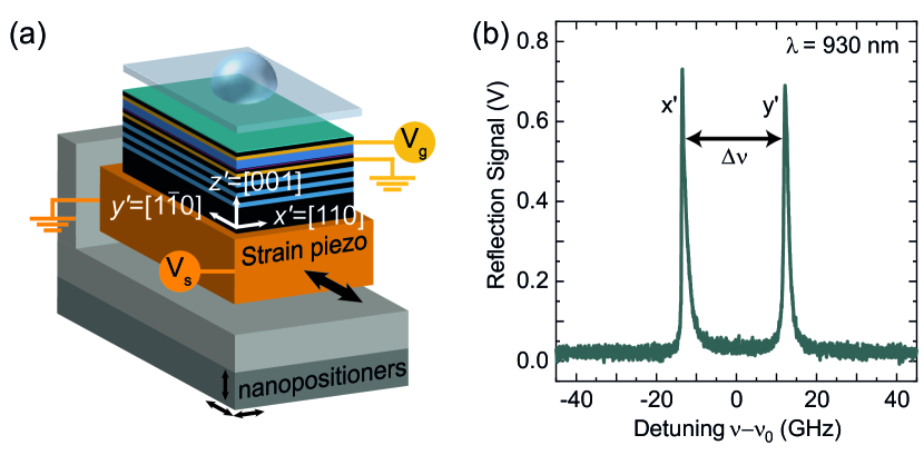
We employ an miniturized Fabry-Pérot cavityBarbour et al. (2011); Greuter et al. (2014); Najer et al. (2019); Tomm et al. (2021). The bottom mirror is a 46-pair AlAs()/GaAs() semiconductor distributed Bragg reflector (DBR) grown on a GaAs substrate, where refers to the wavelength of light in the material. The surface of the semiconductor heterostructure is passivated via an Al2O3 layer Najer et al. (2020). The top mirror is a 15-pair SiO2()/Ta2O5(), Ta2O5-terminated, dielectric DBR where the layers are deposited onto a microcrater in a silica substrate. The semiconductor heterostructure contains a layer of InAs QDs; the QDs themselves are embedded within an n-i-p heterostructure, allowing the QD charge to be controlled via a voltage () applied to the diode Najer et al. (2019); Tomm et al. (2021). The sample is tightly glued onto a piezostack (PSt 150/7x7/7 cryo, Piezomechanik GmbH, Munich), as depicted in Fig. 1(a). The direction of the crystal aligns with the polarization axis of the pieozstack such that application of a voltage to the piezostack induces a -stress in the semiconductor. The spring constant of the sample is small compared to that of the piezostack, , such that the extension of the piezo should be unaffected by the attached semiconductor. The piezo-sample assembly is free to move relative to the top mirror laterally, allowing different positions in the sample to be probed, and vertically, allowing a reflection spectrum of the microcavity to be recorded at fixed laser wavelength. We employ a cross-polarization confocal microscope Kuhlmann et al. (2013), where an added half-wave plate (HWP) allows the probe laser’s polarization to be aligned with one or the other polarized cavity mode. The sample’s orientation relative to the microscope axes is known; the cleaved edges of the semiconductor sample along the and crystalline axes coincide with the microscope orientation to within few degrees. All experiments were carried out at a temperature T = 4 K.
The fundamental cavity mode is probed by measuring the reflectivity of a narrowband laser in a polarization dark-field modus. Two closely spaced modes are observed as shown in Fig. 1(b). When the HWP is set such that the probe laser’s polarization is aligned to (), only the red (blue) detuned resonance is probed. When the HWP is set such that the probe laser is aligned at to the and directions, both cavity modes can be seen (Fig. 1(b)). These are the characteristic features of a birefringence-induced mode-splitting. The fact that the axes of the cavity modes are consistently aligned with the cleaved edges of the sample implies that birefringence arises in the semiconductor heterostructure, and not in the top mirror. Should the origin of the birefringence lie in the top mirror, no link to the crystal axes of the semiconductor would be expected.
The mode-splitting is defined by , where is the resonance frequency. It’s important to note that the mode-splitting has a sign, negative in our case, meaning that the changes in refractive index along the and directions induce a red- and blue-shift, respectively, relative to the original resonance. The dynamic nature of the microcavity allows us to examine simultaneously the mode-splitting (Fig. 2(a),(c)) and the -factor across the microcavity’s stop-band (Fig. 2(b),(d)). Both the bare mode-splitting and the factor have a dependence on wavelength with maximum amplitude centered around nm, at the stop-band center.
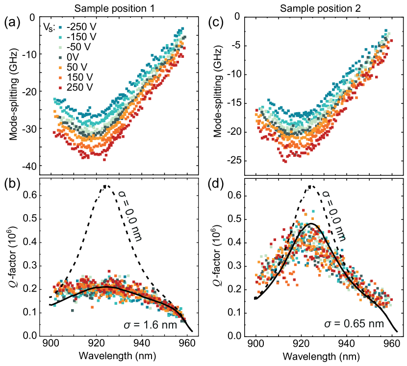
We focus initially on the -factors to demonstrate that we have a quantitative understanding of both the field confinement in the microcavity and the losses. We model the microcavity’s stop-band and -factor dependence on wavelength (Fig. 2(b),(d) dashed and solid lines) using a one-dimensional transfer-matrix simulation (Essential Macleod, Thin Film Center Inc.). In Fig. 2(b),(d) the dashed lines depict the expected -factor without any losses at the sample’s surface. In practice, the measured -factors are lower and this can be described very convincingly simply by including the effects of scattering at the Al2O3-vacuum interface Najer et al. (2020). The surface roughness was determined by comparing the experimental results and the theoretical model. We find that the maximum -factor in this experiment depends on the exact lateral position, suggesting that the surface roughness changes across the sample Najer et al. (2020). A full wavelength dependence was acquired at two positions on the sample. A root-mean-square (rms) surface roughness of nm ( nm) at position 1 (position 2) provide a very good description of the wavelength dependence of the -factor. These surface roughnesses are consistent with characterization of the surface at room temperature with atomic force microscopy Najer et al. (2020). The residual small discrepancy between experimental and modelled curves probably arises from an imperfect knowledge of the exact layer thicknesses in the DBRs.
We turn now to the behaviour on applying a uniaxial stress. We focus on position 1. Upon application of a voltage up to V, the piezostack expands and contracts, thereby stressing the sample uniaxially along the direction. The mode-splitting responds to the applied stress. A maximum mode-splitting tuning of approximately 11 GHz (45 eV) is achieved at the exact wavelength where is the largest, as can be observed in Fig. 2(a). The tuning leaves the -factor unaltered (Fig. 2(b)) indicating that the applied stress has no effect on the loss mechanisms in these high--factor cavities. The mode-splitting is a linear function of (Fig. 3(b)); the response is slightly smaller in magnitude at the edges of the stopband with respect to the stopband center (Fig. 3(d)).
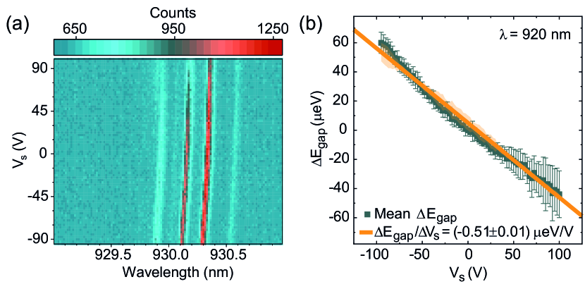
We now attempt to understand quantitatively the stress-induced change in mode-splitting. A crucial step is to determine the exact uniaxial stress applied. The extension per Volt of the piezostack depends strongly on temperature and unfortunately we do not know its exact value at T=4 K. We do not have an external stress gauge in the experiment. Instead, we determine the applied stress by measuring the frequency-shift of the photoluminescence from the QDs embedded in the sample Seidl et al. (2006). This has the advantage of determining the stress experienced by the heterostructure itself, exactly the stress which induces the birefringence. We determine the mean bandgap shift as a function of applied voltage by observing the photoluminescence signal of 20 different excitonic lines in 10 QDs in the sample, as depicted in Fig. 4(a), and find eV/V equivalently GHz/V (Fig 4(b)), a value comparable to a previously achievedSeidl et al. (2006) tuning of eV/V. The dominant effect of uniaxial stress on the emission frequency of the QDs is to induce a change in the bandgap of the host semiconductor GaAs Bhargava and Nathan (1967); Pollak and Cardona (1968); Higginbotham, Cardona, and Pollak (1969), described by . The influence of uniaxial stress on the bandgap can be derived from the material’s deformation potentials to be eV/MPa, under the assumption that the valence state is pure heavy-hole. A detailed calculation is presented in the Appendix. Finally, from
| (1) |
we infer kPa/V, from which we are able to deduce the amount of stress applied to the sample .
The next step is to calculate the birefringence in each layer in the heterostructure. Stress-induced transformations to the dielectric function of a crystal are quantified by the so-called piezobirefringent tensor Nye (1957); Higginbotham, Cardona, and Pollak (1969); Levine et al. (1992); Raynolds, Levine, and Wilkins (1995) . Due to the symmetry of zinc-blende crystals Nye (1957); Raynolds, Levine, and Wilkins (1995), and our system of coordinates , , , the induced birefringence on stressing a semiconductor along by an amount is given by
| (2) |
where is the bare refractive index of the particular material, and is a material parameter, , where is an element of the photoelastic tensor and an element of the compliance tensor. See Appendix for complete derivation.
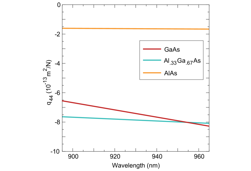
Given that the sample is composed of layers of three different semiconductor materials (GaAs, Al.33Ga.67As and AlAs), the influence of uniaxial stress in each layer must be considered. The coefficients for GaAs, Al.33Ga.67As and AlAs at low temperature T = 4 K are estimated (see Appendix for details) from literature room-temperature values Adachi (1985) and found to be m2/N, m2/N and m2/N respectively.
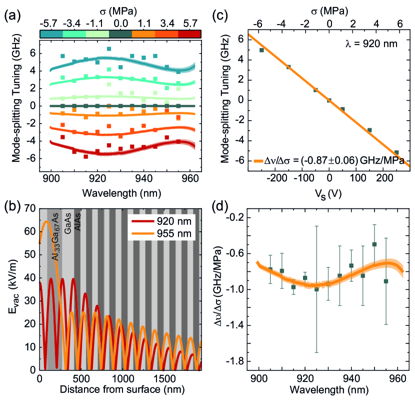
Finally, we determine the mode-splitting by calculating the exact mode frequency for each polarization separately, including the subtle changes to the refractive indexes in the one-dimensional transfer-matrix simulation. Specifically, we use Eq. 2 to calculate the induced birefringence in each layer of the heterostructure upon application of uniaxial stress , which is itself calculated with Eq. 1. For V, MPa, the induced relative birefringence is as small as 26 ppm in GaAs (25 ppm in Al.33Ga.67As, 4 ppm in AlAs). The stress-tuning of the mode-splitting is shown in Fig. 3(a) (solid lines) for each applied stress voltage as a function of wavelength (spanning the stop-band). The results can be directly compared to the experimental results (symbols). Evidently from Fig. 3(a), the amount of tuning itself presents a dispersion, i.e. it depends on wavelength. The calculation captures this detail precisely and explains it: subtle shifts in the standing wave in the microcavity change the net birefringence as each layer of the heterostructure does not contribute equally. Figure 3(b) illustrates this point by showing the vacuum electric field as a function of distance from the sample’s surface at a wavelength close to the stop-band center, at 920 nm, and at a wavelength far away, at 955 nm. As a consequence, the mode-splitting tunes linearly with stress, as depicted in Fig. 3(c) for nm, but with different slopes across the stop-band (Fig. 3(d)). Across the entire spectral range examined here, experimental data (points) and model (solid lines) present excellent agreement.
Our method proves to be an effective way of controlling the intrinsic polarization splitting of an open semiconductor microcavity by up to GHz. The mode-splitting can be tuned across the entire stop-band in a predictable, reversible manner. The present microcavity has a rather large intrinsic mode-splitting. Nevertheless, the tuning capability allows us to achieve near-degeneracy of the cavity modes at the high-wavelength end of the stop-band. For a microcavity with a lower intrinsic mode-splitting, it should be possible to eliminate the mode-splitting. Of relevance here is the fact that the intrinsic mode-splitting and the applied stress are aligned along the same axes. The applied stress induces a small birefringence, on the order of a few ppm, and does not influence the microcavity’s factor. The slight emission shift of the QDs embedded in the heterostructure can be compensated for in the present setup simply by exploiting the spectral tunability of the microcavity: a resonance with the cavity mode is easily maintained.
Naturally, it is desirable to achieve higher degrees of mode-splitting tunability, either to attain perfect degeneracy or to separate fully the two modes. An optimized architecture of the sample holder could increase the tuning rate Zhai et al. (2020) by a factor of 20. The incorporation of a back-gate would allow us to apply an electric field across the bottom mirror, thereby making use of the electrooptic effect Frey et al. (2018). Employing these two methods simultaneously would grant an even higher degree of control of the birefringence. A quantitative understanding of the origin of the intrinsic mode-splitting remains to be attained. However, we note that the mode-splitting dispersion curve can be used as a diagnostic tool, to indicate in which layers of the heterostructure birefringence is strong.
Appendix
.1 Photoelastic effect: the effect of uniaxial stress
The refractive index of a crystal can be described by the indicatrix Nye (1957), an ellipsoid in which the principal axes represent the components of the dielectric tensor,
| (3) |
where is the vacuum’s electric permittivity, is the electric field component along direction and is the electric displacement field along . An applied stress deforms the indicatrix components via the operation
| (4) |
Here, () is the fourth-rank piezo-birefringent tensor; the stress () is a second-rank tensor. From Eq. 3 and Eq. 4, it follows that the change in refractive index (where is the bare refractive index of the isotropic material) reads
| (5) |
For zinc-blende type (cubic) crystals, symmetry simplifies the photoelastic tensor such that only three independent coefficients remain Raynolds, Levine, and Wilkins (1995), namely , and . A compressed notation can be adopted: , , , , , . In this way, the rank of the tensors is reduced and the expression in Eq. 4 becomes (). In extended form,
| (6) |
We now apply these general results to our problem. In the experiment, both the stress and the birefringence are applied/probed in the (,,) system of coordinates. Therefore, a rotation in the frame of reference by around is applied. We treat the canonical case of a stress applied along the direction.
In the (,,) basis, the simplified stress tensor for a uniaxial stress along is self-evidently . We start by calculating in the usual basis (,,) from . The general rotation matrix for an arbitrary angle and with is
| (7) |
In the (,,) basis, the stress is calculated via to be
| (8) |
where is the magnitude of the stress applied. We can now apply Eq. 6 to determine :
| (9) |
Since, however, we want to probe the birefringence in the (,,) basis, we apply the inverse rotation transformation () to determine :
| (10) |
from which follows (using Eq. 5) a change in refractive index
| (11) |
We are primarily interested in the birefringence between axes (,), namely . In the experiment, the stress is applied along . In this case, , and , where in this case has the inverse sign as in the case of stress applied along , from which we obtain Eq. 2.
.2 Bandgap shift with uniaxial stress
In order to calculate the excitonic emission shift as a result of uniaxial stress (along ) we assume that the shift is determined solely by the shift in the bandgap of the host material, GaAs. We start with the Bir-Pikur expression Bir and Pikus (1974) for the bandgap shift with applied strain in the usual basis (,,). The quantum dots themselves define the quantization axis, i.e. . Assuming further that the valence state is of pure heavy-hole character, on account of the large heavy-hole–light-hole splitting,
| (12) |
where and are the deformation potential coefficients, and is the trace of the strain tensor .
We apply a stress, and thereby induce a strain. We use the strain–stress relation , where is the compliance tensor, abbreviated in a similar way to Eq. 6 on account of symmetry. We now know also the expression for a uniaxial stress along in the usual basis (Eq. 8). The strain–stress relation reads
| (13) | ||||
.3 Piezo-optical coefficients at T = 4 K
Data on the piezo-optical coefficient of AlxGa1-xAs alloys can be found for measurements Feldman and Horowitz (1968); Adachi (1985) at K, and for GaAs at K Feldman and Horowitz (1968). However, this data is not available at K to the best of our knowledge. The dispersion of these coefficients is linked to the bandgap of the particular material. In particular, shows a resonance behaviour at the bandgap itself. As the bandgap of these materials shifts with temperature, the coefficients are temperature dependent. It is therefore necessary to estimate the values at K. We elaborate here the procedure.
Adachi Adachi (1985) provides data – we extract the data from the plots with Webplotdigitizer Rohatgi (2020) – on AlxGa1-xAs alloys, of particular relevance here the dispersion curve of the elasto optic coefficients , related to the piezo-birefringent coefficients via . The room-temperature bandgap energies of the alloys of interest are also extracted ((GaAs) eV, (Al.33Ga.67As) eV, (AlAs) eV). The optical properties of semiconductor crystals, such as the refractive index, are linked to the bandgap energy of the material Ravindra, Ganapathy, and Choi (2007). The temperature dependence of the GaAs bandgap can be described via (with in eV, in K) Blakemore (1982). This equation was demonstrated to be valid also for AlxGa1-xAs alloys Lourenço et al. (2001).
From the room-temperature (298 K) bandgap energies, we can estimate the low-temperature bandgap energies of our materials, namely (GaAs) eV, (Al.33Ga.67As) eV, (AlAs) eV, representing a shift in bandgap energy of 95 meV for these materials. These shifts translate into a shift in wavelength of nm, nm and nm, respectively. We now estimate at 4 K for a particular wavelength by rigidly shifting the curve of versus at 298 K by . We confirm that this method functions well by comparing translated K dataAdachi (1985) for to K data Feldman and Horowitz (1968) and verifying an overlap.
Finally, we comment that the dispersion of of the semiconductor materials is rather small in the spectral band of interest, as exemplified in Fig. 5, such that we use their mean values in the model – we treat the small dispersion as a measure of the uncertainty in the parameters.
Acknowledgements.
We thank Liang Zhai for helpful advice on the experimental setup. We acknowledge financial support from SNF project 200020_175748, NCCR QSIT and Horizon-2020 FET-Open Project QLUSTER. A.J. acknowledges support from the European Unions Horizon 2020 Research and Innovation Programme under the Marie Skłodowska-Curie grant agreement No. 840453 (HiFig). S.R.V., R.S., A.L. and A.D.W. acknowledge gratefully support from DFH/UFA CDFA05-06, DFG TRR160, DFG project 383065199, and BMBF Q.Link.X No. 16KIS0867.References
- Wang et al. (2019) H. Wang, Y.-M. He, T. H. Chung, H. Hu, Y. Yu, S. Chen, X. Ding, M. C. Chen, J. Qin, X. Yang, R.-Z. Liu, Z. C. Duan, J. P. Li, S. Gerhardt, K. Winkler, J. Jurkat, L.-J. Wang, N. Gregersen, Y.-H. Huo, Q. Dai, S. Yu, S. Hofling, C.-Y. Lu, and J.-W. Pan, “Towards optimal single-photon sources from polarized microcavities,” Nat. Photonics 13, 770–775 (2019).
- Tomm et al. (2021) N. Tomm, A. Javadi, N. O. Antoniadis, D. Najer, M. C. Löbl, A. R. Korsch, R. Schott, S. R. Valentin, A. D. Wieck, A. Ludwig, and R. J. Warburton, “A bright and fast source of coherent single photons,” Nat. Nanotechnol. (2021).
- Najer et al. (2019) D. Najer, I. Söllner, P. Sekatski, V. Dolique, M. C. Löbl, D. Riedel, R. Schott, S. Starosielec, S. R. Valentin, A. D. Wieck, N. Sangouard, A. Ludwig, and R. J. Warburton, “A gated quantum dot strongly coupled to an optical microcavity,” Nature 575, 622–627 (2019).
- Dousse et al. (2010) A. Dousse, Suffczyński, A. Beveratos, O. Krebs, A. Lemaître, I. Sagnes, J. Bloch, P. Voisin, and P. Senellart, “Ultrabright source of entangled photon pairs,” Nature 466, 217–220 (2010).
- Liu et al. (2019) J. Liu, R. Su, Y. Wei, B. Yao, S. F. C. Silva, Y. Yu, J. Iles-Smith, K. Srinivasan, A. Rastelli, J. Li, and X. Wang, “A solid-state source of strongly entangled photon pairs with high brightness and indistinguishability,” Nat. Nanotechnol. 14, 586–593 (2019).
- Fushman et al. (2008) I. Fushman, D. Englund, A. Faraon, N. Stoltz, P. Petroff, and J. Vučković, “Controlled phase shifts with a single quantum dot,” Science 320, 769–772 (2008).
- Lodahl et al. (2017) P. Lodahl, S. Mahmoodian, S. Stobbe, A. Rauschenbeutel, P. Schneeweiss, J. Volz, H. Pichler, and P. Zoller, “Chiral quantum optics,” Nature 541, 473–480 (2017).
- Söllner et al. (2015) I. Söllner, S. Mahmoodian, S. L. Hansen, L. Midolo, A. Javadi, G. Kiršanskė, T. Pregnolato, E.-E. Haitham, E. H. Lee, J. D. Song, S. Stobbe, and P. Lodahl, “Deterministic photon-emitter coupling in chiral photonic circuits,” Nat. Nanotechnol. 10, 775–778 (2015).
- van Exter, Jansen van Doorn, and Woerdman (1997) M. P. van Exter, A. K. Jansen van Doorn, and J. P. Woerdman, “Electro-optic effect and birefringence in semiconductor vertical-cavity lasers,” Phys. Rev. A 56, 845–853 (1997).
- van der Ziel and Gossard (1977) J. P. van der Ziel and A. C. Gossard, “Absorption, refractive index, and birefringence of AlAs‐GaAs monolayers,” J. Appl. Phys. 48, 3018–3023 (1977).
- Raynolds, Levine, and Wilkins (1995) J. E. Raynolds, Z. H. Levine, and J. W. Wilkins, “Strain-induced birefringence in GaAs,” Phys. Rev. B 51, 10477–10488 (1995).
- Bonato et al. (2009) C. Bonato, D. Ding, J. Gudat, S. Thon, H. Kim, P. M. Petroff, M. P. van Exter, and D. Bouwmeester, “Tuning micropillar cavity birefringence by laser induced surface defects,” Appl. Phys. Lett. 95, 251104 (2009).
- Frey et al. (2018) J. A. Frey, H. J. Snijders, J. Norman, A. C. Gossard, J. E. Bowers, W. Löffler, and D. Bouwmeester, “Electro-optic polarization tuning of microcavities with a single quantum dot,” Opt. Lett. 43, 4280–4283 (2018).
- Gerhardt et al. (2020) S. Gerhardt, M. Moczała-Dusanowska, L. Dusanowski, T. Huber, S. Betzold, J. Martín-Sánchez, R. Trotta, A. Predojević, S. Höfling, and C. Schneider, “Optomechanical tuning of the polarization properties of micropillar cavity systems with embedded quantum dots,” Phys. Rev. B 101, 245308 (2020).
- Seidl et al. (2006) S. Seidl, M. Kroner, A. Högele, K. Karrai, R. J. Warburton, A. Badolato, and P. M. Petroff, “Effect of uniaxial stress on excitons in a self-assembled quantum dot,” Appl. Phys. Lett. 88, 203113 (2006).
- Zhai et al. (2020) L. Zhai, M. C. Löbl, J.-P. Jahn, Y. Huo, P. Treutlein, O. G. Schmidt, A. Rastelli, and R. J. Warburton, “Large-range frequency tuning of a narrow-linewidth quantum emitter,” Appl. Phys. Lett. 117, 083106 (2020).
- Barbour et al. (2011) R. J. Barbour, P. A. Dalgarno, A. Curran, K. M. Nowak, H. J. Baker, D. R. Hall, N. G. Stoltz, P. M. Petroff, and R. J. Warburton, “A tunable microcavity,” J. Appl. Phys. 110, 053107 (2011).
- Greuter et al. (2014) L. Greuter, S. Starosielec, D. Najer, A. Ludwig, L. Duempelmann, D. Rohner, and R. J. Warburton, “A small mode volume tunable microcavity: Development and characterization,” Appl. Phys. Lett. 105 (2014), 10.1063/1.4896415.
- Najer et al. (2020) D. Najer, N. Tomm, A. Javadi, A. R. Korsch, B. Petrak, D. Riedel, S. R. Valentin, R. Schott, A. D. Wieck, A. Ludwig, and R. J. Warburton, “Suppression of surface-related loss in a gated semiconductor microcavity,” arXiv:2012.05104 (2020).
- Kuhlmann et al. (2013) A. V. Kuhlmann, J. Houel, D. Brunner, A. Ludwig, D. Reuter, A. D. Wieck, and R. J. Warburton, “A dark-field microscope for background-free detection of resonance fluorescence from single semiconductor quantum dots operating in a set-and-forget mode,” Rev. Sci. Instrum. 84, 073905 (2013).
- Bhargava and Nathan (1967) R. N. Bhargava and M. I. Nathan, “Stress dependence of photoluminescence in GaAs,” Phys. Rev. 161, 695–698 (1967).
- Pollak and Cardona (1968) F. H. Pollak and M. Cardona, “Piezo-electroreflectance in Ge, GaAs, and Si,” Phys. Rev. 172, 816–837 (1968).
- Higginbotham, Cardona, and Pollak (1969) C. W. Higginbotham, M. Cardona, and F. H. Pollak, “Intrinsic piezobirefringence of Ge, Si, and GaAs,” Phys. Rev. 184, 821–829 (1969).
- Nye (1957) J. F. Nye, Physical Properties of Crystals (Oxford University Press, 1957).
- Levine et al. (1992) Z. H. Levine, H. Zhong, S. Wei, D. C. Allan, and J. W. Wilkins, “Strained silicon: A dielectric-response calculation,” Phys. Rev. B 45, 4131–4140 (1992).
- Adachi (1985) S. Adachi, “GaAs, AlAs, and AlxGa1-xAs: Material parameters for use in research and device applications,” J. Appl. Phys. 58, R1–R29 (1985).
- Bir and Pikus (1974) G. L. Bir and G. E. Pikus, Symmetry and strain-induced effects in semiconductors (Wiley, 1974).
- Burenkov et al. (1973) Y. A. Burenkov, Y. M. Burdukov, S. Y. Davidov, and S. P. Nikaronov, “Temperature dependences of the elastic constants of Gallium Arsenide,” Sov. Phys. Solid State 15, 1175–1177 (1973).
- Van de Walle (1989) C. G. Van de Walle, “Band lineups and deformation potentials in the model-solid theory,” Phys. Rev. B 39, 1871–1883 (1989).
- Sun, Thompson, and Nishida (2007) Y. Sun, S. E. Thompson, and T. Nishida, “Physics of strain effects in semiconductors and metal-oxide-semiconductor field-effect transistors,” J. Appl. Phys. 101, 104503 (2007).
- Feldman and Horowitz (1968) A. Feldman and D. Horowitz, “Dispersion of the piezobirefringence of GaAs,” J. Appl. Phys. 39, 5597–5599 (1968).
- Rohatgi (2020) A. Rohatgi, “Webplotdigitizer: Version 4.3,” (2020).
- Ravindra, Ganapathy, and Choi (2007) N. M. Ravindra, P. Ganapathy, and J. Choi, “Energy gap-refractive index relations in semiconductors - an overview,” Infrared Phys. Technol. 50, 21–29 (2007).
- Blakemore (1982) J. S. Blakemore, “Semiconducting and other major properties of Gallium Arsenide,” J. Appl. Phys. 53, R123–R181 (1982).
- Lourenço et al. (2001) S. A. Lourenço, I. F. L. Dias, J. L. Duarte, E. Laureto, E. A. Meneses, J. R. Leite, and I. Mazzaro, “Temperature dependence of optical transitions in AlGaAs,” J. Appl. Phys. 89, 6159–6164 (2001).