Controlling the TiN electrode work function at the atomistic level: a first principles investigation
Abstract
The paper reports on a theoretical description of work function of TiN, which is one of the most used materials for the realization of electrodes and gates in CMOS devices. Indeed, although the work function is a fundamental quantity in quantum mechanics and also in device physics, as it allows the understanding of band alignment at heterostructures and gap states formation at the metal/semiconductor interface, the role of defects and contaminants is rarely taken into account. Here, by using first principles simulations, we present an extensive study of the work function dependence on nitrogen vacancies and surface oxidation for different TiN surface orientations. The results complement and explain a number of existent experimental data, and provide a useful tool to tailoring transport properties of TiN electrodes in device simulations.
I Introduction
The metal-insulator-metal (MIM) integrated capacitors are key device structures for modern analog and radio frequency integrated circuits hu2002 . This includes both two-terminal devices such as in ovonic selectors chai2019 ; song2019 , and layered gates in connection with high- metal-oxide dielectrics, such as, HfO2 wenger2009 , TiO2nolan2017 , SiO2fonseca2006 ; cottom2019 , and Al2O3du2018 . In this scenario, TiN recently become the reference metal for CMOS compatible gates and MIM devices lukosius2008 . The key feature in the realization of these devices is the alignment between the work function (WF) of the metal contact and the semiconductor band edges. It is generally assumed that TiN has a WF eV, even though this value can be modulated over a large energy range 4.1-5.3 eV, depending on the growth characteristic of the sample, the coupling with semiconductor (e.g. doped Si) or metal-oxide substrates or temperature treatments fillot2005 ; liu2006 ; ren2006 ; westlinder2003 .
TiN crystallizes in a cubic rocksalt structure, and can be easily cleaved along several low-index faces, such as (100), (110), and (111) surfaces. Previous works indicated a net trend in the surface formation energy of the cleavage surfaces, where TiN(100) is the most and TiN(111) is the least stable one marlo2000 . Nonetheless, the growth of single crystal films is unusual and too expensive for any realistic technological application. Almost all TiN-based electrodes and gate contacts are made of polycrystalline films, whose constituting grains have different sizes and expose multiple faces, depending on the conditions and techniques used to grow the samples. In particular, the crystallinity of the substrate strongly affects the morphology, orientation, and resistivity of the films krylov2019 . Different sets of XRD characterizations fillot2005 ; lukosius2008 indicate that in polycrystalline TiN films grown on SiO2 and HfO2 substrates, crystalline grains preferentially expose the (111) face, with minor contribution from the (200) one. Furthermore, in standard growth conditions (i.e. N-poor) TiN forms stable non-stoichiometric crystals (namely TiNx) over a broad composition range x gusev2001 ; khan1999 . A large variety of multi-technique experiments schaffer92 ; patsalas2001 ; fink1984 ; mirguet2006 indicate that in substoichiometric TiNx materials the most recurrent defects are the nitrogen vacancies (VN), and that high VN concentrations remarkably affect the optoelectronic prb_mater ; schmid1998 and the transport properties of the system, including its WFliu2006 . Finally, TiN easily undergoes surface oxidationmilo1995 ; achour2018 : this happens both when as-grown films or fresh cleavage surfaces are exposed to air acs_photonics ; perrier2014 , and when TiN is in contact with other metal oxides.
While the role of interfaces with dielectric layers has been thoroughly studiedwenger2009 ; fonseca2006 ; chen2011 , the intrinsic structural and chemical origins of the WF variability have been rarely taken into account fillot2005 . In this paper, we present a first principles investigation of the effects of surface termination, substoichiometry and oxidation on TiN WF. Our results indicate that the experimental measured WF values are the results of the average combination of all these structural and composition factors. In particular, the control of defect distribution and crystalline grains during growth can be engineered to tailor the transport properties of TiN for specific MIM characteristics.
II Computational Details
DFT calculations for TiN thin films are performed using the Quantum ESPRESSO package espresso . Ab initio ultrasoft pseudopotentials uspp are used to describe the electron-ion interactions and the Perdew-Burke-Ernzerhof (PBE) functional pbe , within the generalized gradient approximation (GGA), is used to treat the exchange-correlation electron interaction. In the pseudopotential description, the following valence electron configurations are considered: N:, O:, and Ti:. Single particle wavefunction and charge are expanded in a plane wave basis set up to an kinetic energy cutoff of 30Ry, and 300 Ry, respectively. Geometry optimizations are carried out with convergence thresholds of 0.03eV/Å for the the forces on each atom. Extensive accuracy tests can be found in previous publications prb_TiN ; omex ; acs_photonics ; prb_mater .
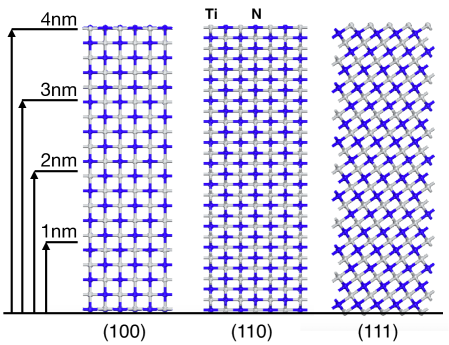
TiN films are simulated by periodic supercells, where we included a thick vacuum layer (Å) in the directions perpendicular to the surface. Each slab contains a variable number of layers with (100), (110) or (111) surface orientation, which cover the thickness range 1.0-4.0 nm (Figure 1). (100) and (110) faces expose an equal number of Ti and N atoms, while (111) surfaces are terminated either with Ti or with N atoms at both slab ends. The layer alternation typical of the [111] stacking of rocksalt structure could impart polar instability to the (111) surface. However, the metallic character of TiN prevents this effects, and no surface reconstruction or non-polar (100) microfacets have been observed in experimental or theoretical reports, confirming that the TiN(111) is a stable surface fillot2005 ; lukosius2008 . In standard N-poor growth conditions, Ti-terminated TiN(111) surface has the lowest surface energy yang2020 ; fan2016 . Thus, TiN(111) surface is modeled via a non-polar off-stoichiometric slab with Ti-termination on both external faces (Figure 1c), in agreement with previous theoretical simulations marlo2000 . No mixed Ti/N terminations of simulated slabs are considered, in order to avoid spurious electric fields in the vacuum region of the cell. N-terminated (111) are not considered in this work, and label (111) will refer only to the Ti-terminated surface. Summations over the surface 2D Brillouin zone is done by using dense k-point grids, which depend on the lateral size of the surface, namely (), (), and (), for (100), (110), and (111), respectively.
Oxide and defective films are obtained starting from a 2 nm-thick TiN reference model, with () and () lateral periodicity for (100) and (111) surface, respectively. Oxide surfaces are prepared by adding oxygen on both outermost layers of TiN slabs (symmetric configuration), as N-substitutional atoms and O2 adsorbed molecules. Defective TiNx systems are simulated including an increasing number of N vacancies (VN) in the reference slabs.
III Results and discussion
III.1 Surface termination
TiN crystalizes in the NaCl lattice structure within the Fm3m space group; the most favored cleavage surfaces are the TiN(100), TiN(110) and Ti-terminated TiN(111) faces. We studied all these surfaces with different thicknesses from 1nm to 4 nm, as shown in Figure 1. After full atomic optimization, all structures undergo only minor relaxations of the outermost layers, in agreement with previous theoretical calculations marlo2000 ; mehmood2015 . Surface relaxation is sufficient to redistribute charge at the surface and to stabilize the structure. The analysis of the projected bandstructures (discussed e.g. in Ref. prb_TiN ) indicates the presence of surface states in restricted regions (lenses) across the edges of the 2D Brillouin zone at high binding energies, while no surface states are present in the proximity of the Fermi level, for any considered surfaces.
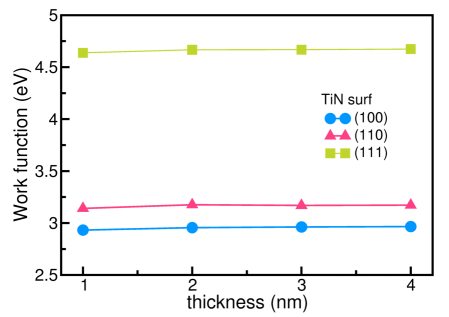
The work function for all systems is calculated as the difference between the Fermi energy resulting from DFT calculations and the vacuum level, extracted from the double averaged electrostatic potential peressi98 . The results (Figure 2) clearly indicate the effect of the surface termination on the WF of TiN. The calculated WF are 2.96 eV, 3.17 eV and 4.67 eV for (100), (110) and (111) faces, respectively. The WF variability is related to the charge accumulation at surface: (100) and (110) have the same number of Ti and N atoms per layer, while (111) has alternative layer of Ti or N atoms, with a large charge accumulation on the Ti outermost layer. Thickness hardly affects the WF that, for all surface orientations, remains almost identical with respect to the number of layers (WF=30 meV). This is due to the the high electron density of TiN ( e/cm-3) prb_TiN , which easily reaches the bulk-like behavior, in agreement with transport and optical measurements on thin TiN films gall2001 ; shah2017 . These results are well representative of polycrystalline films, where the typical grain size is of the order of 2-3 nm fillot2005 as well as of thicker single crystal surfaces acs_photonics . In particular, the predominance of (111) exposed surfaces in polycrystalline systems fillot2005 explains the close agreement of the average experimental WF values ( eV) with the calculated results for the (111) surface.
III.2 Nitrogen vacancies
We investigated the effects of VN in the TiNx(100) and TiNx(111) surface, by considering an increasing number of N vacancies, from 0 to 50% of the total nitrogen amount, in a reference 2nm-thick TiN(100) and TiN(111) surface, respectively. In all cases, the removal of N atoms from TiN surfaces (i.e. inclusion of N vacancies) does not remarkably change the atomic structure, which maintains the characteristic of the ideal (undefective) cubic system. We do not observe any relevant atomic displacement, clusterization, or sub-phase formation in any system, even for extremely high sub-stoichiometric condition (e.g. removal of 50% of nitrogen). This is in agreement with the analysis of N-vacancies in sub-stoichiometric TiNx bulk, reported in Ref. prb_mater . The metallic character of TiN prevents the formation of charged defects and charge accumulation around the defects site, which might be responsible for polaronic distortion.
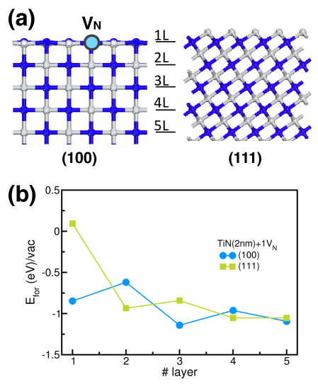
In order to gain insight on the stability of defective surface systems, we studied the formation energy of a single N vacancy as a function of the layer position. As shown in Figure 3a, we considered the first five layers (1L-5L), where 1L identifies the outermost N-layer, while 5L is representative of an inner (i.e. bulk like) layer. The formation energy of nitrogen vacancies is defined as Freysoldt2014 :
| (1) |
where is the total energy of the optimized TiNx defective surface including at layer L, is the total energy of the ideal TiN surface (i.e. no vacancies); is the number of N-atoms being removed from a defect-free cell to its respective reservoir with chemical potential , to form the defective cell. In the case of a single vacancy, . Growth conditions determine the bounds limits for the element chemical potential. In the Ti-rich/N-poor conditions N chemical potential in TiN can be obtained as , where the chemical potential is equal the total energy of TiN bulk (2 atoms per fcc cell) and is the Ti chemical potential extracted from the Ti hcp metal bulk (2 atoms per cell). The simulated formation energy of TiN and substoichiometric TiNx bulk systems have been calculated from first principles in Ref. prb_mater in very good agreement with previous results chase98 .
For TiN(100) the defect formation energy is always negative (Figure 3b), with a damped even-odd oscillation which converge in the bulk to the value -1.1 eV prb_mater , where even layers have the lowest negative formation energies. TiN(111) also exhibits a damped even-odd trend, but in this case odd layers are energetically favored and the first layer has a small but positive formation energy. This behavior can be ascribed to the fact that (111) surface is Ti-terminated, and N atoms lay in subsurface layers (Figure 3a). This general trend confirms that defective TiNx surfaces are stable, and energetically favored, with tiny energy differences in the spatial distribution of N-vacancies, which can be considered uniformly distributed over the entire structure.
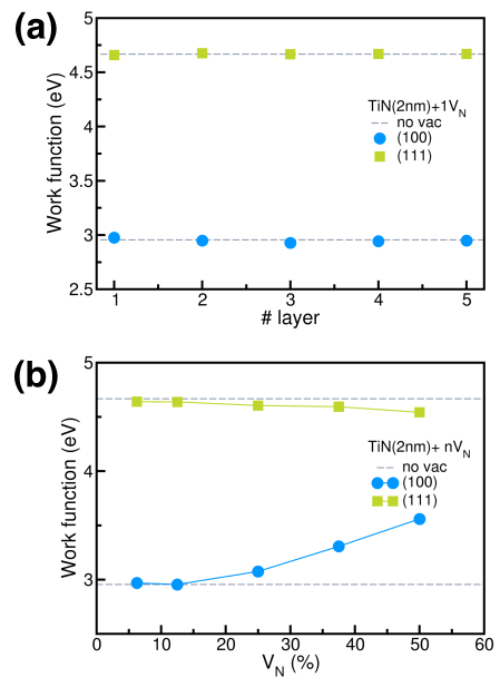
The calculated WFs are shown in Figure 4a, where the corresponding values of undefective TiN surfaces (dashed lines) are superimposed for comparison. In both cases, the inclusion of a single (i.e. very diluted) N-vacancy does not impart any relevant change in the WF of the system. However, when the Ti/N ratio increases as in the experimental systems, WF deviates from the stoichiometric value, as displayed in Figure 4b. The work function of TiNx(100) increases while WF of (111) decreases by hundreds of meV, in agreement with the experimental findings olsson2004 . As the amount of N content is reduced, the WF of both TiNx surfaces approaches the value WF=4.2 eV, which is a fingerprint also of the hcp Ti metal.
This analysis indicates that single WF values, deriving from experiments and used in transport models, are instead results averaged over the full sample, where the surface terminations and the chemical composition play a combined role. The statistical predominance of the (111) surface pins the WF final value close to 4.6 eV. TiN(100) has lower WF, but the presence of N-vacancies shifts WF to higher energy values closer to the (111) surface. The final overall value of a polycrystalline electrode depends on the specific percentage of exposed grain faces and on their composition, and thus on the specific growth conditions. This explains the large variability of the measured WFs. The formation of interfaces with doped semiconductors, of high- metal-oxides may further modify these values fillot2005 ; lima2012 .
III.3 Surface oxidation
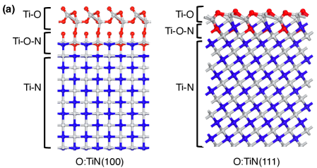
Following the experimental indicationsacs_photonics ; guler2015 we prepared the initial O:TiN structures by including a combination of N-substitutional oxygen atoms and O2 adsorbed molecules on top of TiN(100) and TiN(111) surfaces, in both Ti atop and hollow surface sites. Different atomic configurations could exist depending on the surface preparation, the growth condition and the oxygen amount. In the case of TiN(100) surface, the initial structure included 3 N-substitutional oxygen atoms and 2 O2 molecules. Other combinations of single O atoms and/or O2 molecules have been previously investigated in Ref. acs_photonics . The one presented here best reproduced the transport and optical experimental properties of oxidized ultrathin TiN films shah2017 . The initial O:TiN(111) structure has been prepared along the same line, keeping the same oxygen percentage per TiN atoms of the (100) surface case, and including a mix of N-substitutional and on-surface adsorbed oxygen. After atomic optimization, both systems present a strong surface rearrangement and the formation of a mixed oxynitride layer, as shown in Figure 5a. Oxygen interacts with TiN surfaces, saturating exposed N-vacancies and bonding to outermost Ti atoms. In particular, O2 molecules dissociate to best coordinate with Ti atoms. This leads the formation of TiNxOy layers with different Ti coordinations: one intermediate mixed Ti-O-N layer and one Ti-O external capping layer, in agreement with X-ray experimental analysis acs_photonics ; milo1995 ; braic2017 . A similar feature is observed also in the XPS oxygen signals where it is possible to distinguish N-substitutional, mixed Ti-O-N and pure Ti-O contributions. This implies a different level of coordination of oxygen atoms in the topmost external layers, as shown in Figure 5a. Notably, in agreement with experimental resultssia.740230713 ; zgrabik ; braic , the outermost Ti-O layer does not have the same bonding coordination as in the TiO2 case. The oxidation of TiN to TiO2 is usually observed at high deposition temperature (T900K) and under constant oxygen fluxes.
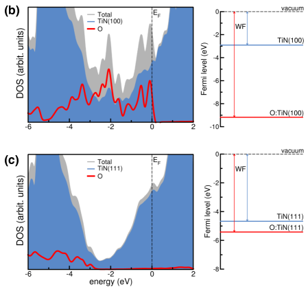
The density of states (DOS) of the resulting systems are shown in Figure 5b-c (left panel). In the case of (100) surface, the higher amount of under-coordinated oxygen contributes to the states close to the Fermi level (EF), while its contribution is negligible in the case of (111) surface, where TiN orbitals dominate the energy range close to EF. This difference is due to the different Ti-coordination in the two surface structures: the coexistence of Ti and N/O in each layer of (100) favors the formation of mixed O-Ti-N bonds. The alternation of Ti and N/O in the (111) structure allows for the formation only of Ti-N and Ti-O bonds at higher binding energies. The different electronic structures affect also the final WFs of the system that now become WF=9.18 eV and WF=5.42 eV, for O:TiN(100) and O:TiN(111), as shown in Figure 5. Surface oxidation causes a blue-shift of WF in both systems, but while the difference with respect to the clean surface is WF=0.75 eV for TiN(111), it is WF=6.30 eV in the case of TiN(100). In the latter case oxygen acts as a capping layer that stabilizes the entire system, in agreement with previous theoretical calculations on MgO layers on TiN (100) surface ren2006 . The further growth of thick metal-oxide layers may mitigate this effect resulting in WF closer to range 4-5 eV, typically assumed for TiN/oxide gate interfaces fillot2005 ; liu2006 ; ren2006 . Thus, the total or partial oxidation of crystal grains constitutes another degree of freedom in the overall WF value of TiN electrodes.
IV Conclusion
We presented a detailed study of the structural, stoichiometric and chemical effects on the work function of intrinsic TiN films, as used in electrode contacts. Our results show that face orientation, N-vacancies and surface oxidations are different causes of modulation of TiN WF, whose final value depends on the details of the growth conditions. The typical predominance of TiNx grains with (111) terminations, is the main origin of the average WF measured in polycrystalline electrodes. The control of the growth conditions can be engineered to obtain a fine tuning of the electrode WF so to optimize the band alignment with the semiconductor elements of the devices.
V Acknowledgments
This work was supported in part by EC through H2020-NMBP-TO-IND project GA n. 814487 (INTERSECT).
References
- (1) H. Hu, C. Zhu, Y. F. Lu, M. F. Li, B.J . Cho, W. K. Choi,“A high performance MIM capacitor using HfO2 dielectrics,” IEEE Electron. Device Lett. vol. 23, pp. 514–516, Oct. 2002.
- (2) Z. Chai, W. Zhang, R. Degraeve, S. Clima, F. Hatem, J. F. Zhang, P. Freitas, J. Marsland, A. Fantini, D. Garbin, L. Goux, and G. Sankar Kar,“Dependence of Switching Probability on Operation Conditions in GexSe1?x Ovonic Threshold Switching Selectors,” IEEE Electron. Device Lett. vol. 40, pp. 1269–1272, Aug. 2019.
- (3) B. Song, H. Xu, S. Liu, H. Liu, Q. Liu, and Q. Li,“An ovonic threshold switching selector based on Se?rich GeSe chalcogenide,” Appl. Phys. A vol. 125, pp. 772, Oct. 2019.
- (4) Ch. Wenger, M. Lukosius, G. Weidner, H.-J. Müssig, S. Pasko, and Ch. Lohe, “The role of the HfO2-TiN interface in capacitance-voltage nonlinearity of Metal-Insulator-Metal capacitors,” Electroch. Acta vol. 141, pp. 25–32, Jul. 2014.
- (5) J. J. Gutiérrez Moreno, and M. Nolan, “Ab Initio Study of the Atomic Level Structure of the Rutile TiO2(110)? Titanium Nitride (TiN) Interface,” ACS Appl. Mater. Inter. vol. 9, pp. 38089–38100, Oct. 2017.
- (6) L. R. C. Fonseca and A. A. Knizhnik, “First-principles calculation of the TiN effective work function on SiO2 and on HfO2,” Phys. Rev. B vol. 74, pp. 195304, Nov. 2006.
- (7) J. Cottom, A. Bochkarev, E. Olsson, K. Patel, M. Munde, J. Spitaler, M. N. Popov, M. Bosman, and A. L. Shluger, “Modeling of Diffusion and Incorporation of Interstitial Oxygen Ions at the TiN/SiO2 Interface,” ACS Appl. Mater. Inter. vol. 11, pp. 36232–36243, Sep. 2019.
- (8) L. Du, H. Wong, S. Dong, W.-S. Lau, and V. Filip, “AFM study on the surface morphologies of TiN films prepared by magnetron sputtering and Al2O3 films prepared by atomic layer deposition,” Vacuum vol. 153, pp. 139–144, Apr. 2018.
- (9) M. Lukosius, C. Wenger, S. Pasko, H.-J. Müssig, B. Seitzinger, and C. Lohe, “Atomic Vapor Deposition of Titanium Nitride as Metal Electrodes for Gate-last CMOS and MIM Devices,” Chem. Vapor Dep. vol. 14, pp. 123–128, Jun. 2008.
- (10) F. Fillot, T. Morel, S. Minoret, I. Matko, S. Maitrejean, B. Guillaumot, B. Chenevier, and T. Billon, “Investigations of titanium nitride as metal gate material, elaborated by metal organic atomic layer deposition using TDMAT and NH3,” Microelect. Eng. vol. 82, pp. 248–253, Dec. 2005.
- (11) Y. Liu, S. Kijima, E. Sugimata, M. Masahara, K. Endo, T. Matsukawa, K. Ishii, K. Sakamoto, T. Sekigawa, H. Yamauchi, Y. Takanashi, and Eiichi Suzuki, “Investigation of the TiN Gate Electrode With Tunable Work Function and Its Application for FinFET Fabrication,” IEEE Trans. Nanotech. vol. 5, pp. 723–730, Nov. 2006.
- (12) C. Ren, B. B. Faizhal, D.S.H. Chan, M.-F. Li, Y.-C. Yeo, A.D. Trigg, N. Balasubramanian, D.-L. Kwong, “Work function tuning of metal nitride electrodes for advanced CMOS devices,” Thin Sol. Films vol. 505, pp. 174–177, May. 2006.
- (13) J. Westlinder, T. Schram, L. Pantisano, E. Cartier, A. Kerber, G. S. Lujan, J. Olsson, and G. Groeseneken, “On the thermal stability of atomic layer deposited TiN as gate electrode in MOS devices,” IEEE Electron. Device Lett. vol. 24, pp. 550–552, Sep. 2003.
- (14) M. Marlo and V. Milman, “Density-functional study of bulk and surface properties of titanium nitride using different exchange-correlation functionals,” Phys. Rev. B vol. 62, pp. 2899–2907, Jul. 2000.
- (15) I. Krylov, X. Xu, Y. Qi, K. Weinfeld, V. Korchnoy, M. Eizenberg, and D. Ritter, “Effect of the substrate on structure and properties of titanium nitride films grown by plasma enhanced atomic layer deposition,” J. Vac. Sci. Technol. A vol. 37, pp. 060905, Sep. 2019.
- (16) A. I. Gusev, A. A. Rempel, and A. J. Magerl ” Disorder and Order in Strongly Nonstoichiometric Compounds Springer, Heidelberg 2001.
- (17) J. H. Kang, and K. J. Kim, “Structural, optical, and electronic properties of cubic TiNx TiNx compounds,” J. Appl. Phys. vol. 86, pp. 346–350, Jun. 1999.
- (18) J. P. Schaffer, A. J. Perry, and J. Brunner, “Defects in hard coatings studied by positron annihilation spectroscopy and x?ray diffraction,” J. Vac. Sci. Technol. A vol. 10, pp. 193–207, Jan. 1992.
- (19) P. Patsalas, and S. Logothetidisr, “Optical, electronic, and transport properties of nanocrystalline titanium nitride thin films,” J. Appl. Phys. vol. 90, pp. 4725–4734, Nov. 2001.
- (20) J. Pflüger, J. Fink, W. Weber, K. P. Bohnen, and G. Crecelius, “Dielectric properties of , , , and from 1.5 to 40 eV determined by electron-energy-loss spectroscopy,” Phys. Rev. B vol. 30, pp. 1155–1163, Aug. 1984.
- (21) C. Mirguet, L. Calmels, and Y. Kihn, “Electron energy loss spectra near structural defects in TiN and TiC,” Micron vol. 37, pp. 442–448, Jul. 2006.
- (22) A. Catellani, P. D’Amico, and A. Calzolari, “Tailoring the plasmonic properties of metals: The case of substoichiometric titanium nitride,” Phys. Rev. Mater. vol. 4, pp. 015201, Jan. 2020.
- (23) P. E. Schmid, M. S. Sunaga, and F. Lévy, “Optical and electronic properties of sputtered thin films,” J. Vac. Sci. Technol. A vol. 16, pp. 2870–2875, May. 1998.
- (24) I. Milošv, H.-H. Strehblow, B. Navinšek, and M. Metikoš?Huković, “Electrochemical and thermal oxidation of TiN coatings studied by XPS,” Surf. Interf. Analysis vol. 23, pp. 529–539, Jul. 1995.
- (25) A. Achour, M. Islam, I. Ahmad, L. Le Brizoual, A. Djouadi, and T. Brousse, “Influence of surface chemistry and point defects in TiN based electrodes on electrochemical capacitive storage activity,” Scripta Materialia vol. 153, pp. 59–62, May. 2018.
- (26) D. Shah, A. Catellani, H. Reddy, N. Kinsey, V. Shalaev, A. Boltasseva, and A. Calzolari, “Controlling the Plasmonic Properties of Ultrathin TiN Films at the Atomic Level,” ACS Photonics vol. 5, pp. 2816–2824, May 2018.
- (27) A. Seifitokaldania, O. Savadogo, and M. Perrier, “Density Functional Theory (DFT) Computation of the Oxygen Reduction Reaction (ORR) on Titanium Nitride (TiN) Surface,” This Sol. Films vol. 517, pp. 6334–6336, Feb. 2009.
- (28) C.-L. Chen, and Y.-C. King, “TiN Metal Gate Electrode Thickness Effect on BTI and Dielectric Breakdown in HfSiON-Based MOSFETs,” IEEE Trans. Elecron. Dev vol. 58, pp. 3736–3742, Nov. 2011.
- (29) P. Giannozzi, O. Andreussi, T. Brumme, O. Bunau, M. Buongiorno Nardelli, M. Calandra, R. Car, C. Cavazzoni, D. Ceresoli, M. Cococcioni, N. Colonna, I. Carnimeo, A. D. Corso, S. de Gironcoli, P. Delugas, R. A. DiStasio, A. Ferretti, A. Floris, G. Fratesi, G. Fugallo, R. Gebauer, U. Gerstmann, F. Giustino, T. Gorni, J. Jia, M. Kawamura, H.-Y. Ko, A. Kokalj, E. K uckbenli, M. Lazzeri, M. Marsili, N. Marzari, F. Mauri, N. L. Nguyen, H.-V. Nguyen, A. O. de-la Roza, L. Paulatto, S. Poncé, D. Rocca, R. Sabatini, B. Santra, M. Schlipf, A. P. Seitsonen, A. Smogunov, I. Timrov, T. Thonhauser, P. Umari, N. Vast, X. Wu, and S. Baroni, “Advanced capabilities for materials modelling with Quantum ESPRESSO,” J. Phys.: Condens. Matter vol. 29, pp. 465901, Oct. 2017.
- (30) D. Vanderbilt,“Soft self-consistent pseudopotentials in a generalized eigenvalue formalism,” Phys. Rev. B vol. 41, pp. R7892–R7895, Apr. 1990.
- (31) J. P. Perdew, K. Burke, and M. Ernzerhof, “Generalized Gradient Approximation Made Simple,” Phys. Rev. Lett. vol. 77, pp. 3865–3868, Oct. 1996.
- (32) A. Catellani and A. Calzolari, “Plasmonic properties of refractory titanium nitride,” Phys. Rev. B vol. 95, pp. 115145, Mar. 2017.
- (33) A. Catellani and A. Calzolari, “Tailoring the plasmonic properties of ultrathin TiN films at metal-dielectric interfaces,” Opt. Mater. Exp. vol. 9 pp. 1458–1458, Mar. 2019.
- (34) T. Yang, M. Wei, Z. Ding, X. Han, and J. Li, “Ab initio calculations on the Mg/TiN heterogeneous nucleation interface,” J. Phys. Chem. Sol. vol. 143, pp. 109479, Apr. 2020.
- (35) X. Fan, B. Chen, M. Zhang, D. Li, Z. Liu, and C. Xiao, “First-principles calculations on bonding characteristic and electronic property of TiC (111)/TiN (111) interface,” Mater. & Design. vol. 112, pp. 282–289, Dec. 2016.
- (36) F. Mehmood, R. Pachter, N. R. Murphy, and W. E. Johnson, “Electronic and optical properties of titanium nitride bulk and surfaces from first principles calculations,” J. Appl. Phys. vol. 118, pp. 195302, Nov. 2015.
- (37) M Peressi and N Binggeli and A Baldereschi, “Band engineering at interfaces: theory and numerical experiments,” J. Phys.D: Appl. Phys. vol. 31, pp. 1273–1299, Jun. 1998.
- (38) D. Shah, H. Reddy, N. Kinsey, V. M. Shalaev, and A. Boltasseva, “Optical Properties of Plasmonic Ultrathin TiN Films,” Adv. Opt. Mater. vol. 5, pp. 1700065, May 2017.
- (39) D. Gall, I.Petrov, and J. E. Greene, “Epitaxial Sc1?xTixN(001): Optical and Electronic Transport Properties,” J. Appl. Phys. vol. 89, pp. 401–409, Jan. 2001.
- (40) C. Freysoldt, B. Grabowski, T. Hickel, J. Neugebauer, G. Kresse, A. Janotti and C. G. Van de Walle,“First-principles calculations for point defects in solids,” Micron vol. 86, pp. 253–304, Jan.-Mar. 2014.
- (41) M. W. Chase Jr.“First-principles calculations for point defects in solids, J. Phys. Chem. Ref. Data, Monograph vol. 9, 1–1951 1998.
- (42) J. Westlinder, G. Sjöblom, and J. Olsson, “Variable work function in MOS capacitors utilizing nitrogen-controlled TiNx gate electrodes,” Microelect. Eng. vol. 75, pp. 389–396, Aug. 2004.
- (43) L. P. B. Lima, J. A. Diniz, I. Doi, and J. Godoy Fo, “Titanium nitride as electrode for MOS technology and Schottky diode: Alternative extraction method of titanium nitride work function,” Microelect. Eng. vol. 92, pp. 86–90, Apr. 2012.
- (44) U. Guler, S. Suslov, A. V. Kildishev, A. Boltasseva, and V. M. Shalaev, “Colloidal Plasmonic Titanium Nitride Nanoparticles: Properties and Applications,” Nanophotonics vol. 4, pp. 269–276, Jun 2015.
- (45) L. Braic, N. Vasilantonakis, A. Mihai, I. J. Villar Garcia, S. Fearn, B. Zou, N. McN. Alford, B. Doiron, R. F. Oulton, S. A. Maier, A. V. Zayats, and P. K. Petrov, “Titanium Oxynitride Thin Films with Tunable Double Epsilon-Near-Zero Behavior for Nanophotonic Applications,” ACS Appl. Mater. Inter. vol. 9, pp. 29857–29862, Aug 2017.
- (46) I. Milosv̌, H.-H. Strehblow, B. Navinsěk, and M. Metikoš-Huković. “Electrochemical and Thermal Oxidation of TiN Coatings Studied by XPS,” Surf. Interface Anal. vol. 23, pp. 529–539, Jul 1995.
- (47) C. M. Zgrabik, and E. L. Hu, “Optimization of Sputtered Titanium Nitride as a Tunable Metal for Plasmonic Applications,” Opt. Mater. Express vol. 5, pp. 2786–2797, Nov. 2015.
- (48) L. Braic, N. Vasilantonakis, A. Mihai, I. J. Villar Garcia, S. Fearn, B. Zou, N. M. Alford, B. Doiron, R. F. Oulton, S. A. Maier, A. V. Zayats, and P. K. Petrov, “Titanium Oxynitride Thin Films with Tunable Double Epsilon-Near- Zero Behavior for Nanophotonic Applications,” ACS Appl. Mater. Interfaces vol. 9 , pp. 29857–29862, Aug. 2017.